
SEGA Confidential
General Notice
When using this document, keep the following in mind:
1. This document is confidential. By accepting this document you acknowledge that you are bound
by the terms set forth in the non-disclosure and confidentiality agreement signed separately and /in
the possession of SEGA. If you have not signed such a non-disclosure agreement, please contact
SEGA immediately and return this document to SEGA.
2. This document may include technical inaccuracies or typographical errors. Changes are periodi-
cally made to the information herein; these changes will be incorporated in new versions of the
document. SEGA may make improvements and/or changes in the product(s) and/or the
program(s) described in this document at any time.
3. No one is permitted to reproduce or duplicate, in any form, the whole or part of this document
without SEGA'S written permission. Request for copies of this document and for technical
information about SEGA products must be made to your authorized SEGA Technical Services
representative.
4. No license is granted by implication or otherwise under any patents, copyrights, trademarks, or
other intellectual property rights of SEGA Enterprises, Ltd., SEGA of America, Inc., or any third
party.
5. Software, circuitry, and other examples described herein are meant merely to indicate the character-
istics and performance of SEGA's products. SEGA assumes no responsibility for any intellectual
property claims or other problems that may result from applications based on the examples
describe herein.
6. It is possible that this document may contain reference to, or information about, SEGA products
(development hardware/software) or services that are not provided in countries other than Japan.
Such references/information must not be construed to mean that SEGA intends to provide such
SEGA products or services in countries other than Japan. Any reference of a SEGA licensed prod-
uct/program in this document is not intended to state or simply that you can use only SEGA's
licensed products/programs. Any functionally equivalent hardware/software can be used instead.
7. SEGA will not be held responsible for any damage to the user that may result from accidents or any
other reasons during operation of the user's equipment, or programs according to this document.
(6/27/95- 002)
NOTE: A reader's comment/correction form is provided with this
document. Please address comments to :
SEGA of America, Inc., Developer Technical Support (att. Evelyn Merritt)
150 Shoreline Drive, Redwood City, CA 94065
SEGA may use or distribute whatever information you supply in any way
it believes appropriate without incurring any obligation to you.
|

SEGA Confidential
TM
© 1994 SEGA. All Rights Reserved.
SCU
User's Manual
Third version
Doc. # ST-97-R5-072694
|

SEGA Confidential
READER CORRECTION/COMMENT SHEET
Chpt.
pg. #
Correction
Corrections:
General Information:
Your Name
Phone
Document number
Date
Document name
Questions/comments:
Keep us updated!
If you should come across any incorrect or outdated information while reading through the attached
document, or come up with any questions or comments, please let us know so that we can make the
required changes in subsequent revisions. Simply fill out all information below and return this form to
the Developer Technical Support Manager at the address below. Please make more copies of this form if
more space is needed. Thank you.
Fax:
(415) 802-3963
Attn: Manager,
Developer Technical Support
Mail:
SEGA OF AMERICA
Attn: Manager,
Developer Technical Support
275 Shoreline Dr. Ste 500
Redwood City, CA 94065
Where to send your corrections:
ST-97-R5-072694
SCU User's Manual
|

SEGA Confidential
REFERENCES
In translating/creating this document, certain technical words and/or phrases were interpreted
with the assistance of the technical literature listed below.
1.
KenKyusha New Japanese-English Dictionary
1974 Edition
2.
Nelson's Japanese-English Character Dictionary
2nd revised version
3.
Microsoft Computer Dictionary
4.
Japanese-English Computer Terms Dictionary
Nichigai Associates
4th version
|

SEGA Confidential
Version History
Version 1:
April 7, 1994
· New draft
Version 2:
May 31, 1994
· Revisions according to April 28, 1994 meeting
Version 3:
July 15, 1994
· Revisions requested on June 30 and July 11, 1994
|

SEGA Confidential
Introduction
This manual explains functions of the system controller and how they are used. The system
controller transfers data rapidly and smoothly by means of the bus controls.
Explanation of Terms
The following terms are used in this manual.
SCU
System Control Unit. The SCU contains the CPU I/F, A-Bus IF, B-BUS I/F, and
smoothly effects data transfers between several processors connected through
their respective I/F and bus. It also internally houses the DMA controller,
interrupt controller, and DSP, and makes possible rapid DMA control, interrupt
control, and processing of operations.
Main CPU
Uses a RISC type CPU SH2 that controls the overall system. SH2 contains 32-bit
internal and external buses.
VDP1
Video Display Processor 1. Functions include character and line painting, color
indication, Gouraud Shading color operations, screen output coordinate indica-
tion, and frame buffer display control.
VDP2
Video Display Processor 2. Functions include scrolling the
screen up/down/
left/right, rotating the screen, determining priority order of multiple screens, and
a priority function that controls the image process of color operations and color
offset.
SCSP
Acronym for Saturn Custom Sound Processor. This is a sound source LSI for
multi-functional games that combines a PCM sound source and sound used for
the DSP.
i
|

SEGA Confidential
SMPC
System Manager and Peripheral Control. Has the functions of managing system
resets, control of interfacing with output devices (control pads, mouse, etc.), time
display by a real time clock, and battery backup.
Data
A bit is the smallest unit for expressing 1 or 0. 8 bits is a byte. 16 bits (or 2 bytes)
is a word. 32 bits (or 4 bytes) is a 9 long word.
A_Bus
Bus that connects external devices such as a ROM cassette or CD.
B_Bus
Bus that connects VDP1, VDP2, and SCSP.
ii
|

SEGA Confidential
Manual Notations
This manual contains the following notations.
Binary
Represented by "
B
" at the end as in 100
B
. However, "
B
" may be omitted
for 1 bit.
Hexadecimal
Represented by
H
at the end as in 00
H
and FF
H
.
Unit
1 KByte is 1,024 bytes. 1 Mbit is 1,048,576 bits.
MSB, LSB
The configuration of byte and word shows at the left the high order bit
(MSB, most significant bit), and atthe right the low order bit (LSB, least
significant bit).
Undefined Bit
A bit not defined by an instruction word is represented by "--"
(R)
Represents read only data.
(W)
Represents write only data.
(R/W)
Represents data that can be read and written.
++
Shows increments. For example, when the CT0 register is incremented, it
is shown as CT0++.
x=2-0
This indicates that 3 types exist, 2,1, and 0. For example, DxR26-0[x=2-0]
in the read address in section 3.2 "DMA Control Register" means that
D2R26-0, D1R26-0, and D0R26-0 exist. Similarly, D2R26-0 indicates that
D2R26 ~ D2R0 exist.
iii
|

SEGA Confidential
CONTENTS
INTRODUCTION
Explanation of Terms .............................................................................. (i)
Manual Notations .................................................................................. (iii)
List of Figures ................................................................................
(vii)
List of Tables ....................................................................................
(x)
CHAPTER 1 OVERVIEW
.......................................................................... 1
1.1 SCU Overview ........................................................................
2
System Diagram ............................................................................. 2
Block Diagram ................................................................................ 3
1.2 SCU Mapping ......................................................................... 4
Operation of Cache Hit ................................................................... 5
1.3 SCU Register Map ................................................................. 7
Level 2-0DMA Set Register ........................................................... 8
DMA Forced-Stop Register ........................................................... 8
DMA Status Register ......................................................................9
DSP Program Control Port ............................................................ 9
DSP Program RAM Data Port ..................................................... 10
DSP Data RAM Address Port ...................................................... 10
DSP Data RAM Data Port ............................................................ 10
Timer 0 Compare Register ........................................................... 11
Timer 1 Set Data Register ............................................................ 11
Timer 1 Mode Register ................................................................. 11
Interrupt Mask Register ................................................................ 12
Interrupt Status Register ...............................................................12
A-Bus Interrupt Acknowledge Register ........................................ 12
A-Bus Set Register ....................................................................... 13
A-Bus Refresh Register ................................................................ 13
SCU SDRAM Select Register ...................................................... 14
SCU Version Register ................................................................... 14
iv
|

SEGA Confidential
CHAPTER 2 OPERATION ...............................................................
15
2.1 DMA Transfer .......................................................................
16
Basic Operation of DMA ...............................................................16
DMA Mode .................................................................................... 18
Example of a Specific Use ............................................................ 21
2.2 Interrupt Control ..................................................................
27
Blanking Interrupt ......................................................................... 29
Timer Interrupt .............................................................................. 30
DSP-End Interrupt ........................................................................ 33
Sound-Request Interrupt .............................................................. 33
SMPC Interrupt ............................................................................. 33
PAD Interrupt ................................................................................ 33
DMA End Interrupt ........................................................................ 33
DMA-Illegal Interrupt ..................................................................... 33
Sprite Draw End Interrupt .............................................................33
2.3 DSP .......................................................................................
34
DSP Control from the Main CPU ................................................. 34
CHAPTER 3 REGISTERS ...............................................................
39
3.1 Register List .........................................................................
40
3.2 DMA Control Registers .......................................................
41
Level 2-0 DMA Set Register ........................................................ 41
DMA Mode, Address Update, Start Factor Select Register ......... 46
DMA Force-Stop Register ............................................................ 47
DMA Status Register .................................................................... 47
3.3 DSP Control Ports ...............................................................
51
DSP Program Control Port .......................................................... 51
DSP Program RAM Data Port ..................................................... 53
DSP Data RAM Address Port ...................................................... 53
DSP Data RAM Data Port ............................................................ 54
3.4 Timer Registers ...................................................................
55
Timer 0 Compare Register .......................................................... 55
Timer 1 Set Data Register ............................................................ 55
Timer 1 Mode Register ................................................................. 56
v
|

SEGA Confidential
3.5 Interrupt Control Registers
..................................................... 57
Interrupt Mask Register ................................................................ 57
Interrupt Status Register ...............................................................58
3.6 A-Bus Control Registers
.......................................................... 61
A-Bus Interrupt Acknowledge Register ........................................ 61
A-Bus Set Register ...................................................................... 62
A-Bus Refresh Register ................................................................ 72
3.7 SCU Control Registers
.............................................................. 73
SCU SDRAM Select Register ...................................................... 73
SCU Version Register ................................................................... 73
CHAPTER 4 DSP CONTROL ..........................................................
75
4.1 DSP Internal BLOCK MAP ..................................................
76
4.2 List of Commands
..................................................................... 80
4.3 Operand Execution Methods ..............................................
85
Jump Command Execution ......................................................... 85
Loop Command Execution .......................................................... 86
DMA Command Execution .......................................................... 87
End Command Execution .............................................................88
4.4 Special Process Execution
..................................................... 89
Loading a Program by the DMA Command ................................. 89
Repeating One Command ............................................................ 89
Executing a Subroutine Program ................................................. 90
4.5 More About Commands
............................................................ 91
Operation Commands .................................................................. 91
Load Immediate Command ....................................................... 120
DMA Command .......................................................................... 132
Jump Commands ....................................................................... 141
Loop Bottom Commands ............................................................ 153
END Command .......................................................................... 156
vi
|

SEGA Confidential
List of Figures
(Chapter 1 Overview)
Figure 1.1 Diagram of System .................................................................................... 2
Figure 1.2 Block Diagram ........................................................................................... 3
Figure 1.3 SCU Mapping (Cache_address) ............................................................. 4
Figure 1.4 Explanation of Cache Hit Operation ........................................................ 5
Figure 1.5 SCU Mapping (Cache_through_address) ................................................. 6
Figure 1.6 SCU Register Map .................................................................................... 7
Figure 1.7 Level 2-0 DMA Set Register Map ............................................................. 8
Figure 1.8 DMA Force-Stop Register Map .................................................................8
Figure 1.9 DMA Status Register Map ......................................................................... 9
Figure 1.10 DSP Program Control Port Map ............................................................. 9
Figure 1.11 DSP Program RAM Data Port Map ....................................................... 10
Figure 1.12 DSP Data RAM Address Port Map ....................................................... 10
Figure 1.13 DSP Data RAM Data Port Map .............................................................10
Figure 1.14 Timer 0 Compare Register Map ............................................................ 11
Figure 1.15 Timer 1 Set Data Register Map ............................................................. 11
Figure 1.16 Timer 1 Mode Register Map .................................................................. 11
Figure 1.17 Interrupt Mask Register Map ................................................................. 12
Figure 1.18 Interrupt Status Register Map ................................................................ 12
Figure 1.19 A-Bus Interrupt Acknowledge Map ....................................................... 12
Figure 1.20 A-Bus Set Register Map
.................................................................. 13
Figure 1.21 A-Bus Refresh Register Map ................................................................. 13
Figure 1.22 SCU SDRAM Select Register Map ....................................................... 14
Figure 1.23 SCU Version Register Map .................................................................. 14
(Chapter 2 Operation)
Figure 2.1 DMA Transfer Basic Operation ................................................................ 16
Figure 2.2 DMA Transferable Area when Activacted from the Main CPU ................ 17
Figure 2.3 DMA Transferable Area when Activacted from the DSP ......................... 17
Figure 2.4 Direct Mode DMA Transfer Operation .................................................... 18
Figure 2.5 Indirect Mode DMA Transfer Flow .......................................................... 19
Figure 2.6 Indirect Mode DMA Transfer Operation Details ...................................... 20
Figure 2.7 Differences in DMA Operations according to the Address Update Bit .... 22
vii
|

SEGA Confidential
Figure 2.8 Example of Data Write ............................................................................ 23
Figure 2.9 Work RAM Area Contents ...................................................................... 24
Figure 2.10 DMA Transfer by Setting Address Add Value ........................................ 26
Figure 2.11 Blanking Interrupt .................................................................................... 29
Figure 2.12 Timer 0 Interrupt Process (compare register = when 19 is set) ........... 30
Figure 2.13 Timer 1 Interrupt Process (In sync with Timer 0) .................................. 31
Figure 2.14 Timer 1 Interrupt Process (not in sync with Timer 0) ............................ 32
Figure 2.15 DSP Program Load Step 1 .................................................................... 34
Figure 2.16 DSP Program Load Step 2 .................................................................... 35
Figure 2.17 DSP Program Load Step 3 .................................................................... 35
Figure 2.18 DSP Data Access Step 1 ....................................................................... 36
Figure 2.19 DSP Data Access Step 2 ...................................................................... 37
Figure 2.20 DSP Data Access Step 3 ...................................................................... 37
Figure 2.21 DSP Program Execution Start Control from CPU ................................. 38
Figure 2.22 DSP Program Forced Stop Control from CPU ...................................... 38
(Chapter 3 Registers)
Figure 3.1 Level 2-0 Read Address (Register: D0R, D1R, D2R) ........................... 41
Figure 3.2 Level 2-0 Write Address (Register: D0W, D1W, D2W) ......................... 41
Figure 3.3 Level 0 Transfer Byte Number (Register: D0C) .................................... 42
Figure 3.4 Level 2-1 Transfer Byte Number (Register: D1C, D2C) ........................ 42
Figure 3.5 Level 2-0 Address Add Value (Register: D0AD, D1AD, D2AD) ............. 42
Figure 3.6 Communication Units between the SCU and Processor ........................ 44
Figure 3.7 Specific Example of Transfer between the SCU and Processor ............. 44
Figure 3.8 Write Address Add Value Indication ........................................................ 45
Figure 3.9 Level 2-0 DMA Authorization Bit (Register: D0EN, D1EN, D2EN) ....... 45
Figure 3.10 Level 2-0 DMA Mode, Address Update, Start Up Factor
Select Register (Register: D0MP, D1MP, D2MP) ................................ 46
Figure 3.11 DMA Force-Stop Register (Register: DSTP) ...................................... 47
Figure 3.12 High and Low Level DMA Operation .................................................... 48
Figure 3.13 DMA Status Register (Register: DSTA) .............................................. 48
viii
|

SEGA Confidential
Figure 3.14 DSP Program Control Port (Register: PPAF) ..................................... 51
Figure 3.15 DSP Program RAM Data Port (Register: PPD) ................................... 53
Figure 3.16 DSP Data RAM Address Port (Register: PDA) .................................... 53
Figure 3.17 DSP Data RAM Data Port (Register: PDD) ........................................ 54
Figure 3.18 Time 0 Compare Register (Register: T0C) ....................................... 55
Figure 3.19 Timer 1 Set Data Register (Register: T1S) ......................................... 55
Figure 3.20 Timer 1 Mode Register (Register: T1MD) ........................................... 56
Figure 3.21 Interrupt Mask Register (Register: IMS) ............................................. 57
Figure 3.22 Interrupt Status Register (Register: IST) ........................................... 58
Figure 3.23 A-Bus Interrupt Acknowledge Register (Register: AIAK) ...................... 61
Figure 3.24 A-Bus Set [CS0, 1 Space] (Register: ASR0) ........................................ 62
Figure 3.25 A-Bus Set [CS2, Dummy Space] (Register: ASR1) ............................. 62
Figure 3.26 Result of Previous Read Process ......................................................... 63
Figure 3.27 Timing when Setting the Pre-Charge Insert Bit after Write ................... 63
Figure 3.28 Timing when Setting the Pre-Charge Insert Bit after Read .................. 64
Figure 3.29 Differences in Timing by Setting External Wait Effective Bit ................. 64
Figure 3.30 A-Bus Refresh Register (Register: AREF) .......................................... 72
Figure 3.31 SCU SDRAM Select Bit (Register: RSEL) .......................................... 73
Figure 3.32 SCU Version Register (Register: VER) ................................................ 73
Chapter 4 DSP Control)
Figure 4.1 DSP Internal Block Map ........................................................................... 77
Figure 4.2 Jump Command Execution ..................................................................... 85
Figure 4.3 Loop Program Execution ......................................................................... 86
Figure 4.4 Subroutine Program Execution ................................................................ 91
Figure 4.5 Operation Command Format ................................................................... 92
Figure 4.6 Load Immediate Command Format 1 (Unconditional Transfer) ........... 120
Figure 4.7 Load Immediate Command Format 2 (Conditional Transfer) ............... 120
Figure 4.8 DMA Command Format 1 ...................................................................... 132
Figure 4.9 DMA Command Format 2 ...................................................................... 132
Figure 4.10 Jump Command Format ...................................................................... 141
Figure 4.11 Loop Bottom Command Format ......................................................... 153
Figure 4.12 End Command Format ........................................................................ 156
ix
|

SEGA Confidential
List of Tables
(Chapter 2 Operation)
Table 2.1 Interrupt Factors ................................................................. 27
Table 2.2 Interrupt Factor General Names ........................................ 28
(Chapter 3 Registers)
Table 3.1 Register List ....................................................................... 40
Table 3.2 Read Address Add Value ................................................... 43
Table 3.3 Write Address Add Value ................................................... 43
Table 3.4 Starting Factors .................................................................. 46
Table 3.5 RAM Page Select ...............................................................53
Table 3.6 Timer 1 Occurrence Selection Contents ............................ 56
Table 3.7 Timer Operation Contents ................................................. 56
Table 3.8 Interrupt Status Bit Contents ............................................. 59
Table 3.9 A-Bus Interrupt Acknowledge Contents .............................. 61
Table 3.10 CS0 Space Burst Cycle Set Values .................................. 65
Table 3.11 CS0 Space Normal Cycle Set Values ............................... 65
Table 3.12 CS0 Space Burst Length Set Values ................................ 65
Table 3.13 CS0 Space Bus Size Set Values ...................................... 66
Table 3.14 CS1 Space Burst Cycle Set Values .................................. 67
Table 3.15 CS1 Space Normal Cycle Set Values ............................... 67
Table 3.16 CS1 Space Burst Length Set Values ................................ 68
Table 3.17 CS1 Space Bus Size Set Values ...................................... 68
Table 3.18 CS2 Space Burst Cycle Set Values .................................. 69
Table 3.19 CS2 Space Bus Size Set Values ...................................... 70
Table 3.20 Dummy Space Burst Cycle Set Values ............................. 71
Table 3.21 Dummy Space Normal Cycle Set Values ......................... 71
Table 3.22 Dummy Space Burst Length Set Values ........................... 71
Table 3.23 Dummy Space Bus Size Set Values ................................. 72
Table 3.24 A-Bus Refresh Wait Number ............................................. 72
x
|

SEGA Confidential
(Chapter 4 DSP Control)
Table 4.1 List of Commands (1) ........................................................ 80
Table 4.2 List of Commands (2) ........................................................ 81
Table 4.3 List of Commands (3) ........................................................ 82
Table 4.4 List of Commands (4) ........................................................ 83
Table 4.5 Descriptions of Constants .................................................. 84
Table 4.6 Features of Data Transfer from D0 Bus to DSP ................ 87
Table 4.7 Features of Data Transfer from DSP to D0 Bus ................ 88
xi
|

SEGA Confidential
SCU User's Manual
1
CHAPTER 1 OVERVIEW
Chapter 1 Contents
1.1
SCU Overview ......................................................................2
System Diagram ..................................................2
Block Diagram .....................................................3
1.2
SCU Mapping .......................................................................4
Operation of Cache Hit ......................................5
1.3
SCU Register Map................................................................7
Level 2-0DMA Set Register ................................8
DMA Forced-Stop Register ................................8
DMA Status Register ..........................................9
DSP Program Control Port ................................9
DSP Program RAM Data Port .........................10
DSP Data RAM Address Port ..........................10
DSP Data RAM Data Port ................................10
Timer 0 Compare Register ............................... 11
Timer 1 Set Data Register ................................. 11
Timer 1 Mode Register ..................................... 11
Interrupt Mask Register ...................................12
Interrupt Status Register ..................................12
A-Bus Interrupt Acknowledge Register ........12
A-Bus Set Register .............................................13
A-Bus Refresh Register .....................................13
SCU SDRAM Select Register ...........................14
SCU Version Register ........................................14
|

SEGA Confidential
2
1.1
SCU Overview
The SCU (System Control Unit) contains a CPU I/F, A-Bus I/F, and B-Bus I/F. It
smoothly interfaces multiple processors connected through their respective I/Fs and
buses. Also contained inside are the DMA controller, interrupt controller, and DSP.
The DMA controller controls the internal level 2-0 as well as DSP total 4 channel
DMA transfer, and allows the free transfer of data between the CPU, A-Bus, and B-
Bus. Using the CPU-Bus, the CPU can access the work area while executing the
DMA of the A-Bus and B-Bus. The DSP region must be used in data transfer request
from the DSP. For instance, DMA transfer with the A-Bus and B-Bus not using the
DSP region cannot request that data be transfered from the DSP.
The interrupt controller includes interrupts from the A-Bus, B-Bus, and System
Manager, and controls all interrupts within the SCU. It also supports interrupt by
timers and can produce interrupts that are in sync with the screen.
DSP can handle processes that cannot be handled by the main CPU when its load
has been exceeded. DSP operates at half the frequency of the main CPU. As a result,
one step takes about 70 nsec.
System Diagram
A diagram of the system is shown in Figure 1.1. The Work RAM-H, Work RAM-L,
Backup RAM, IPL ROM, and SMPC are connected to the CPU-Bus. The CPU-Bus
controls the system reset signal and control pad. The medium that supplies the CD
or cartridge software is an external system connected to the A-Bus. VDP1, VDP2,
and SCSP are connected to the B-Bus and control picture and sound.
SCU
INT Signal
CPU-Bus
WORK
RAM-H
IPL
ROM
SMPC
VDP1
VDP2
SCSP
A-Bus
B-Bus
WORK
RAM-L
BACKUP
RAM
Main
CPU
Figure 1.1 Diagram of System
|

SEGA Confidential
SCU User's Manual
3
Block Diagram
A block diagram of the SCU is shown in Figure 1.2. As previously mentioned, the
CPU interface, A-Bus, and B-Bus interfaces, and the DMA controller, interrupt con-
troller, and DSP are contained in the SCU. All interfaces and controllers are con-
nected by buses, making transfer of data possible.
The CPU I/F and A-Bus I/F connections are through two buses. The upper bus is
connected through the register. The lower bus is a connection used in transferring
data. Therefore, DMA transfer is done using the lower bus.
DSP
INT
TIMER
CPU
I/F
DMA
A-Bus
I/F
B-Bus
I/F
A-Bus
B-Bus
Main CPU
SCU
CPU-Bus
Figure 1.2 Block Diagram
|
SEGA Confidential
4
1.2
SCU Mapping
Figure 1.3 shows the mapping operation.
Figure 1.3 SCU Mapping (Cache_address)
ROM Access Region
External Area 1 Region
VDP 1 Region
SCU Register Region
00000000
H
02000000
H
05900000
H
04000000
H
05000000
H
05800000
H
05A00000
H
05C00000
H
05E00000
H
05FC0000 H
05FE0000
H
06000000
H
07FFFFFF
H
512 Kbyte
32 Mbyte
16 Mbyte
8 Mbyte
1 Mbyte
1 Mbyte
about 1 Mbyte
1 Mbyte
192 Kbyte
512 Kbyte
~
~
00080000
H
VDP 1 Region
VDP 2 Region
VDP 2 Region
VDP 2 Region
24 byte
4 byte
288 byte
208 byte
Indicates areas that can't be accessed
05B00EE4
H
05CC0000
H
05D00000
H
05D00018
H
05E80000
H
05F00000
H
05F01000
H
05F80000
H
05F80120
H
05FE00D0
H
06100000
H
01800004
H
01800000
H
01000004
H
01000000
H
00300000
H
00200000
H
00190000
H
00180000
H
00100080
H
00100000
H
A-Bus CS1 Region
A-Bus Dummy Region
A-Bus CS0 Region
A-Bus CS2 Region
SMPC Region
Backup-RAM Region
Work-RAM-L Region
MINIT Region
SINIT Region
Sound Region
VDP 2 Region
SCU Register Region
Work RAM-H Region
4 byte
1 Mbyte
128 byte
64 Kbyte
4 Kbyte
|

SEGA Confidential
SCU User's Manual
5
Operation of Cache Hit
If a hit is made to the cache during access to an area that is rewritable by non-CPU
devices such as the work RAM of an I/O port, an external device, or a SCU register,
a value different from the actual value could be returned. When this happens, the
cache-through area must be accessed.
Figure 1.4 explains cache hit operations, and Figure 1.5 shows cach-through opera-
tions.
Cache
SCU
A Device
B Device
CPU
Cache
SCU
CPU
Cache
SCU
CPU
Cache
SCU
CPU
A Device
B Device
A Device
B Device
arrow indicates the flow of data
Data read from device B
Write from device A to B (DMA)
Accesses cache address area
Accesses cache-through area
Reads address 5C00000
H
Data is FFFFFFFF
H.
CPU can write data to cache
Cache does not change.
B Device
A Device
Address 5C00000
H
clears to 0
Address 5C00000
H
is read again.
Data FFFFFFFF
H
inside cache
becomes valid.
Reads again from device B without
accessing the cache. Data is 0.
Address is 25C00000
H
.
Figure 1.4 Explanation of Cache Hit Operation
|

SEGA Confidential
6
ROM Access Region
External Area 1 Region
VDP 1 Region
SCU Register Region
20000000
H
22000000
H
25900000
H
24000000
H
25000000
H
25800000
H
25A00000
H
25C00000
H
25E00000
H
05FC0000 H
25FE0000
H
26000000
H
27FFFFFF
H
512 Kbyte
32 Mbyte
16 Mbyte
8 Mbyte
1 Mbyte
1 Mbyte
about 1 Mbyte
1 Mbyte
192 Kbyte
512 Kbyte
~
~
20080000
H
VDP 1 Region
VDP 2 Region
VDP 2 Region
VDP 2 Region
24 byte
4 byte
288 byte
208 byte
Indicates areas that can't be accessed
25B00EE4
H
25CC0000
H
25D00000
H
25D00018
H
25E80000
H
25F00000
H
25F01000
H
25F80000
H
25F80120
H
25FE00D0
H
26100000
H
21800004
H
21800000
H
21000004
H
21000000
H
20300000
H
20200000
H
20190000
H
20180000
H
20100080
H
20100000
H
A-Bus CS1
A-Bus Dummy
A-Bus CS0
A-Bus CS2
SMPC Region
Backup-RAM Region
Work-RAM-L Region
MINIT Region
SINIT Region
Sound Region
VDP 2 Region
SCU Register Region
Work RAM-H Region
4 byte
1 Mbyte
128 byte
64 Kbyte
4 Kbyte
Figure 1.5 SCU Mapping (Cache_through_address)
|

SEGA Confidential
SCU User's Manual
7
1.3
SCU Register Map
Figure 1.6 shows a map of the SCU register. The SCU register is assigned to the
highest address in the SCU mapping region and, as shown in Figure 1.3, maintains a
208 byte area. Next, a map of each register region is shown.
Figure 1.6 SCU Register Map
DMA Forced Stop
25FE0000
H
25FE0020
H
25FE0060
H
32 byte
32 byte
16 byte
4 byte
25FE0040
H
32 byte
Level 2 DMA Set Register
25FE0070
H
16 byte
DMA Status Register
DSP Program Control Port
DSP Program RAM DataPort
4 byte
4 byte
DSP Data RAM Address Port
DSP Data RAM DataPort
4 byte
4 byte
Timer 0 Compare Register
Timer 1 Set Data Register
4 byte
4 byte
Timer 1 Mode Register
Free
4 byte
4 byte
Interrupt Mask Register
Interrupt Status Register
4 byte
A-Bus Interrupt Acknowledge
Free
4 byte
Level 1 DMA Set Register
Level 0 DMA Set Register
4 byte
A-Bus Set Register
8 byte
A-Bus Refresh Register
Free
4 byte
SCU SDRAM Select Register
SCU Version Register
4 byte
Free
25FE0080
H
25FE0084
H
25FE0088
H
25FE008C
H
25FE0090
H
25FE0094
H
25FE0098
H
25FE00A0
H
25FE00A4
H
25FE00A8
H
25FE00B0
H
25FE009C
H
25FE00B8
H
25FE00BC
H
25FE00C4
H
25FE00C8
H
25FE00CC
H
25FE00CF
H
4 byte
8 byte
4 byte
25FE00AC
H
|

SEGA Confidential
8
Level 2-0 DMA Set Register
Figure 1.7 is a map of the Level 2-0 DMA set register. Parameters required for DMA
transfer are stored in this register. There are three DMA levels (from level 0 to level
2), as there are in the SCU register map (Figure 1.6). As a result, the addresses in
Figure 1.7 are shown as relative addresses.
31
24
0
Read Address (in bytes)
16
8
Write Address (in bytes)
Transfer byte number (in bytes)
(R/W)
(R/W)
(R/W)
(W)
(W)
(W)
1
2
4
3
5
6
7
00
H
04
08
0C
10
14
18
1C
H
H
H
H
H
H
H
8
Inside graphic:
1. Read address add value 5. DMA mode bit (=0:Direct Mode / =1:Indirect Mode)
2. Write address add value
6. Read address update bit (=0:Save / =1:Revise)
3. DMA enable bit (=0:Disable / =1:Enable) 7. Write address update bit (=0:Save / =1:Update )
4. DMA starting bit
8. DMA start factor select bit
Figure 1.7 Level 2-0 DMA Set Register Map
DMA Force-Stop Register
Figure 1.8 is a map of the DMA force-stop register. This register has a bit that forces
the DMA operation to stop. However, if the DMA is forced to stop, it can no longer
be used. This register should not be used except for debugging.
31
0
(W)
1
H
25FE0060
Inside graphic:
1. DMA force-stop bit (=1:DMA force-stop)
Figure 1.8 DMA Force-Stop Register Map
|

SEGA Confidential
SCU User's Manual
9
DMA Status Register
Figure 1.9 is a map of the DMA status register. This register shows level 2-0 condition
status.
31
24
0
16
8
(R)
1 2
H
3
4 5
6 7
8 9
1011
13
25FE007C
12
Inside graphic:
1. DMA DSP-Bus access flag (=0: no access /=1:access)
2. DMA B-Bus access flag (=0: no access / =1:access) 8. Level 1 DMA standby (=0:stop/=1:standby)
3. DMA A-Bus access flag (=0: no access / =1:access) 9. Level 1 DMA in operation (=0:stop/=1:operate)
4. Level 1 DMA interrupt(=0:stop/=1:interrupt)
10. Level 0 DMA stand by (=0:stop/=1:standby)
5. Level 0 DMA interrupt(=0:stop/=1:interrupt)
11. Level 0 DMA in operation (=0:stop/=1:operate)
6. Level 2 DMA standby (=0:stop/=1:standby)
12. DSP side DMA in stand by (=0:stop/=1:standby)
7. Level 2 DMA in operation (=0:stop/=1:operate)
13. DSP side DMA in operation (=0:stop/=1:operate)
Figure 1.9 DMA Status Register Map
DSP Program Control Port
Figure 1.10 is a map of the DSP program control port. This is the DSP control register.
It stores both the DSP operation start address and end address.
31
0
(R/W)
1 2
3 4 5 6 7 8 91011
Prog RAM address
26
24
16 15
7
H
25FE0080
Inside graphic:
1. EX = cancels pause briefly (=0: no execute/=1:execute) 7. Overflow flag
2. EX = executes pause briefly (=0: no execute/=1:execute) 8. Program end interrupt flag
3. D0 bus use DMA transfer execution flag
4. Sine flag
9. Program step execute control bit (=0:no execute/=1:execute)
5. Zero flag
10. Program execute control (=0:stop/=1:execute)
6. Carry flag
11. Program counter load authorization (=0:no execute/=1:execute)
Figure 1.10 DSP Program Control Port Map
|

SEGA Confidential
10
DSP Program RAM Data Port
Figure 1.11 is a map of the DSP program RAM data port. This port is used as a
go-between when transferring program data from the CPU to the DSP.
31
0
(W)
H
05FE0084
Program RAM Data
Figure 1.11 DSP Program RAM Data Port Map
DSP Data RAM Address Port
Figure 1.12 is a map of the DSP data RAM address port. This port indicates the data
RAM address while accessing the data RAM inside DSP from the CPU.
31
0
(W)
H
05FE0088
Data RAM Address
7
Figure 1.12 DSP Data RAM Address Port Map
DSP Data RAM Data Port
Figure 1.13 is a map of the DSP data RAM data port. The content of the address
shown by the DSP data RAM address port is stored. Data written from the CPU is
stored in the DSP data RAM and data read from the CPU can fetch RAM data inside
the DSP.
31
0
(R/W)
H
05FE008C
Data RAM Data
Figure 1.13 DSP Data RAM Data Port Map
|

SEGA Confidential
SCU User's Manual
11
Timer 0 Compare Register
Figure 1.14 is the map of the timer 0 compare register. Timer 0 gets in sync with V-
Blank-IN interrupt (See 2.2 Interrupt Control) and causes interrupt to occur. The opera-
tion is explained in section 2.2 and the register contents are explained in chapter 3.
31
0
(W)
H
05FE0090
Counter Value
9
Figure 1.14 Timer 0 Compare Register Map
Timer 1 Set Data Register
Figure 1.15 is the map timer 1 set data register. Timer 1 is data-set by H-Blank-IN inter-
rupt (See 2.2 Interrupt Control) and decremented by 7 MHz cycles. Interrupt occurs
when data is 0. The operation is explained in section 2.2 and the register contents are
explained in chapter 3.
31
0
(W)
H
05FE0094
Set Data
8
Figure 1.15 Timer 1 Set Data Register Map
Timer 1 Mode Register
Figure 1.16 is a map of the timer 1 mode register. This register indicates the timing by
which Time 1 is generated. The operation is explained in section 2.2 and the register
contents are explained in chapter 3.
31
0
(W)
H
05FE0098
2
8
Inside graphic:
1. Timer 1 mode bit
=0:occurs at each line
=1:occurs only for lines designated by timer 0
2. Time operation enable bit
=0: Timer operation OFF
=1 : Timer operation ON
Figure 1.16 Timer 1 Mode Register Map
|

SEGA Confidential
12
Interrupt Mask Register
Figure 1.17 shows the map of the interrupt mask register. When this bit is 0, interrupt
is not masked and occurs as needed. When the bit is 1, interrupt will not occur be-
cause it is masked. Chapter 3 has more information about bit 0 (inside graphic, no. 15)
to bit 13 (inside graphic, no. 2).
31
0
(W)
H
05FE00A0
15
14
13
12
11
10
9
8
7
6
5
4
3
2
1
15
Inside graphic:
1. A-Bus interrupt mask bit
2~15 Interrupt mask bit
Figure 1.17 Interrupt Mask Register Map
Interrupt Status Register
Figure 1.18 shows the map of the interrupt status register. Because this register is able
to read and write, when reading it shows that interrupt won't occur when bit data is 0,
and will occur when bit data is 1. When writing, interrupt is reset if 0 is written, and
maintains the current interrupt status when 1 is written. See chapter 3 for details
about this register.
31
0
(R/W)
H
05FE00A4
15
14
13
12
11
10
9
8
7
6
5
4
3
2
1
16
171819 2021222324 252627282930
Inside graphic:
1~30 Interrupt status bit
Figure 1.18 Interrupt Status Register Map
A-Bus Interrupt Acknowledge Register
Figure 1.19 shows a map of the A-Bus interrupt acknowledge. This is a read/write bit
that has different meanings when reading vs. when writing. See chapter 3 for details.
31
0
(R/W)
H
25FE00A8
1
Inside graphic:
1. READ: A-Bus interrupt acknowledge significant bit (=0:insignificant / =1:significant)
WRITE: A-Bus interrupt acknowledge significant bit (=0:insignificant / =1:significant)
Figure 1.19 A-Bus Interrupt Acknowledge Register Map
|
SEGA Confidential
SCU User's Manual
13
A-Bus Set Register
Figure 1.20 shows the map of the A-Bus set register. Each pre-read significant bit,
precharge insertion bit, and external wait significant bit is insignificant at 0 and
significant at 1. See chapter 3 for more information.
31
0
(W)
H
25FE00B0
15
14
13
12
11
10
9
8
7
6
5
4
3
2
1
16171819 20 21222324
H
25FE00B4
(W)
2526272829
30
31323334
3536
3738394041424344 454647484950 51
52
Inside graphic:
1. CS0 space, pre-read significant bit
31. CS2 space, pre-read significant bit
2. CS0 space, precharge insertion bit after write
32. CS2 space, precharge insertion bit after write
3. CS0 space, precharge insertion bit after read
33. CS2 space, precharge insertion bit after read
4. CS0 space, external wait significant bit
34. CS2 space, external wait significant bit
5~8. CS0 space, burst cycle wait no. set
35~36. CS2 space, burst length set bit
9~12. CS0 space, single cycle wait no. set
37. Bus size set bit (0=16 bit 1=8 bit)
13~14. CS0 space, burst length set
38. Spare space, pre-read significant bit
15. CS0 space, bus size set bit (0=16bit 1=8bit)
39. Spare space, precharge insertion after write
16. CS1 space, pre-read significant bit
40. Spare space, precharge insertion after read
17. CS1 space, precharge insertion bit after write
41. Spare space, external wait significant bit
18. CS1 space, precharge insertion bit after read
42~45. Spare space, burst cycle wait no. set bit
19. CS1 space, external wait significant bit
46~49. Spare space, normal cycle wait no. set bit
20~23. CS1 space, burst cycle wait no. set
50~51. Spare space, burst length set bit
24~27. CS1 space, normal cycle wait no. set
52. Spare space, bus size set bit (0=16bit 1=8bit)
28~29. CS1 space, burst length set bit
30. CS1 space, bus size set bit (0=16bit 1=8bit)
Figure 1.20 A-Bus Set Register Map
A-Bus Refresh Register
Figure 1.21 shows the map of the A-Bus refresh register. This register performs the
settings for A-Bus refresh.
31
0
(W)
H
25FE00B8
4
1 2 3 4 5
Inside graphic:
1. A-Bus refresh output significant bit (=0:insignificant / =1:significant)
2~5. A-Bus refresh wait number set bit
Figure 1.21 A-Bus Refresh Register Map
|

SEGA Confidential
14
SCU SDRAM Select Register
Figure 1.22 shows the map of the SCU SDRAM select register.
31
0
(R/W)
H
25FE00C4
1
Inside graphic:
1. Work-SDRAM select bit (=0:2 Mbit x2 / =1:4 Mbit x 2)
Figure 1.22 SCU SDRAM Select Register Map
SCU Version Register
Figure 1.23 shows the map of the SCU version register.
31
0
(R)
H
25FE00C8
1 2 3 4
Inside graphic:
1~4. Version number`
Figure 1.23 SCU Version Register Map
|

SEGA Confidential
SCU User's Manual
15
CHAPTER 2 OPERATION
Chapter 2 Contents
2.1
DMA Transfer .......................................................................................16
Basic Operation of DMA ...........................................................16
DMA Mode .................................................................................18
Example of A Specific Use ........................................................21
2.2
Interrupt Control ..................................................................................27
Blanking Interrupt ......................................................................29
Timer Interrupt ...........................................................................30
DSP-End Interrupt .....................................................................33
Sound-Request Interrupt ...........................................................33
SMPC Interrupt ..........................................................................33
PAD Interrupt .............................................................................33
DMA End Interrupt ...................................................................33
DMA-Illegal Interrupt ...............................................................33
Sprite Draw End Interrupt ........................................................33
2.3
DSP .......................................................................................................34
DSP Control from the Main CPU .............................................34
|

SEGA Confidential
16
2.1
DMA Transfer
Basic Operation of DMA
Figure 2.1 shows basic DMA operation. This DMA is basically long word access
through the DMA controller buffer, but if the start address and end address are not
in long word boundaries, reads and writes are made in byte units, and DMA transfer
can be executed.
Figure 2.1 is an example of DMA transfer from transfer source address 1H - 50H to
transfer destination address 6H - 55H. However, since the long word boundary in
the transfer source is 4H, 1H - 3H is read in byte units. Since the long word bound-
ary in the transfer destination is 8H, the first 2 bytes of read data are written to 6H -
7H in byte units. Moreover, the transfer source end address is 50H, but since the
long word boundary is up to 4FH, the data in 50H is read in byte units. On the other
hand, since the transfer destination end address is 55H but the long word boundary
is up to 53H, the last two bytes read are written to 54H - 55H in byte units.
Figure 2.1 DMA Transfer Basic Operation
1st byte
2nd byte
3rd byte
4th byte
5th byte
6th byte
7th byte
8th byte
9th byte
75th byte
76th byte
77th byte
78th byte
79th byte
80th byte
~
~
~
~
1st byte
2nd byte
3rd byte
4th byte
5th byte
6th byte
7th byte
8th byte
9th byte
75th byte
76th byte
77th byte
78th byte
79th byte
80th byte
~
~
~
~
Source
Buffer
Destination
read
write
1
H
9
H
8
H
7
H
6
H
5
H
4
H
3
H
2
H
4B
H
4C
H
4E
H
4F
H
4D
H
50
H
1st byte
2nd byte
3rd byte
4th byte
5th byte
6th byte
7th byte
8th byte
9th byte
75th byte
76th byte
77th byte
78th byte
79th byte
80th byte
~
~
~
~
6
H
E
H
D
H
C
H
B
H
A
H
9
H
8
H
7
H
50
H
51
H
53
H
54
H
52
H
55
H
Access in long word units
Access in bytes
|

SEGA Confidential
SCU User's Manual
17
There are two methods of activating the SCU's DMA transfer control.
1) activate DMA from the Main CPU
2) activate DMA from the DSP
Figure 2.2 shows the DMA transferable area when activated from the main CPU.
Figure 2.3 shows the DMA transferable area when activated from the DSP.
Work RAM-H Area
A-Bus Connection
Processor
B-Bus Connection
Processor
Figure 2.2 DMA Transferable Area when activated from the Main CPU
DSP Area
A-Bus Connection
Processor
B-Bus Connection
Processor
Work RAM-H Area
Figure 2.3 DMA Transferable Area when activated from the DSP
|

SEGA Confidential
18
DMA Mode
The SCU DMA mode has the following two modes:
1) Direct Mode
2) Indirect Mode
Direct Mode
Data is transferred only in byte numbers shown as transfer byte numbers directly
using address values of separate level DMA set registers, and from the address
memory shown by the read address register to the address memory shown by the
written address register. One transfer is implemented per start up, then DMA ends.
Figure 2.4 shows the DMA transfer operation of the direct mode.
DMA Set Register
Transfer Byte Number
Address Add Value
DMA Authorization Bit
Mode, Update, Select
Read Address
Write Address
.
.
.
.
Transfer Destination
.
.
.
.
Transfer Source
Write
Address
Read
Address
DMA Transfer
Figure 2.4 Direct Mode DMA Transfer Operation Map
|

SEGA Confidential
SCU User's Manual
19
Indirect Mode
The indirect mode implements DMA transfer by indirectly using the DMA set regis-
ter at a level different from the Direct mode mentioned earlier. The address value
and byte number stored by the Direct mode in the set register are stored in the
indirect mode temporary buffer by the Indirect mode, and DMA transfer is repeated
until the end code is detected. Thus, the Indirect mode can implement more than
one DMA transfer when activated once. Figure 2.5 shows the execution flow of
Indirect mode DMA.
Parameters used for transfer are
copied in a temporary buffer
End Code Exists
DMA Transfer
End
Indirect Mode DMA
DMA Transfer
Y
N
Figure 2.5 Indirect Mode DMA Transfer Flow
|

SEGA Confidential
20
When the Indirect mode is activated, parameters of a 3 long word segment from the
address first written in the write address register (DxW) is read and stored in a
temporary buffer. Next, the actual DMA is executed using the parameters. On
completion of DMA, the address parameters of DxW+C
H
are read and similarly
executed. This operation is repeated until the end code is detected.
The indirect mode address is incremented in 4 byte units.
Figure 2.6 Indirect Mode DMA Transfer Operation Details
DMA Set Register
Address Add Value
DMA Authorization Bit
Mode, Update, Select
Write Address
Transfer Destination
Transfer Source
Read
Address 1
1st DMA Transfer
Temporary Buffer
Transfer Byte Number
Read Address
Write Address
Execute Address Storage Buffer
Write Address
First Transfer Byte Number
First Read Address
First Write Address
Second Transfer Byte Number
Second Read Address
Second Write Address
nth Write Address
nth Transfer Byte Number
Address
(DxW)
(DxW+C
H
)
End Code
(DxW+C(N-1)
H
)
~
~
~
~
2nd DMA Transfer
3rd DMA Transfer
Read
Address 2
Read
Address 3
Write
Address 1
Write
Address 2
Write
Address 3
End of DMA Transfer
|

SEGA Confidential
SCU User's Manual
21
Example of a Specific Use
Direct Mode
A 1 Kbyte transfer can be thought of as level 0 DMA from address 2000000
H
(A-Bus
area) to address 6000000
H
(work RAM). DMA (direct mode) can be executed when
operating in accordance with the following procedures.
1)
Write the read address (200000
H
) to the read address register D0R. (Loads the
address that is read to address 25EF0000
H
from the CPU.)
2)
Write the write address (6000000H) to the write address register D0W. (Loads
the address that is written to address 25EF0004
H
from the CPU.)
3)
Write the transfer byte number (400H) to transfer byte number register D0C.
(Loads the transfer byte number from the CPU to address 25EF0008
H
.)
4)
Write the address add value (101H) to address add value register D0AD.
(Loads the address add value from the CPU to address 25EF000CH. Details of
the address add value are listed in the address add value of this section. The
address add value indicated in the normal DMA is 101H. )
5)
The DMA mode is 0, and the address update bit and DMA start factor are set as
necessary and written to mode/address/update/DMA start factor register
D0MD. For example, when address update is handled as the save mode and
V-Blank-IN is handled as the start factor, 0 is written to D0MD. (Loads 0 in
address 25EF0014H from the CPU.)
6)
Set 1 in the DMA enable bit. When the start factor set by step 5) occurs, DMA
is activated and 1 Kbyte of data is transferred by level 0 from address 2000000
H
(A-Bus area) to address 6000000
H
(work RAM).
7)
After DMA has ended, DMA is activated each time the start factor set in step 5)
occurs. The operation at that time changes according to the values of the read
address update bit (D0RUP) and write address update bit (D0WUP). Figure 2.7
shows DMA operation changes by the address update bit.
Steps 1) to 5) do not have to be done in the same order. (When the start factor is set
in the DMA starting bit, DMA starts each time the DMA operation bit is set to 1 by
the CPU.)
|

SEGA Confidential
2000000
H
20003FF
H
6000000
H
60003FF
H
2000000
H
20003FF
H
6000000
H
6000400
H
When D0RUP=0 and D0WUP=0
When D0RUP=0 and D0WUP=1
2000000
H
2000400
H
When D0RUP=1 and D0WUP=0
6000000
H
60003FF
H
When D0RUP=1 and D0WUP=1
2000000
H
2000400
H
6000000
H
6000400
H
First DMA transfer
Second DMA transfer
22
When the read address update bit is 0, the same address is referred to (read to) both
the first and second time. When the read address update bit is 1, the second read
starts after the address following the first read.
When the write address update bit is 0, write is executed to the same address for
both the first and second time. When the write address update bit is 1, the second
write starts after the address following the first write.
Figure 2.7 Differences in DMA Operations according to the Address update Bit
|

SEGA Confidential
SCU User's Manual
23
Indirect Mode
The Indirect mode is used when executing DMA transfer more than once by starting
once. The Indirect mode is not set in a register as is the Direct mode, but uses a
method of executing DMA by accessing the register through RAM. For example,
consider a case in which three DMA transfers are to be continuously (consecutively)
executed at level 0 through work RAM area (6000000
H
).
(a) 20
H
Byte DMA transfer from 4000000
H
to 5C00000
H
(b) 10
H
Byte DMA transfer from 5E00000
H
to 6080000
H
(c) 15
H
Byte DMA transfer from 5A00000
H
to 6081000
H
DMA (Indirect mode) can be executed if operated in accord with the following steps.
1) As shown in Figure 2.8, data is written in long word units from the work RAM
area (6000000
H
).
4 00 0 00 0
H
5 C0 0 00 0
H
2 0
H
5 E00 0 00
H
6 08 0 00 0
H
1 0
H
5 A00 0 00
H
6 08 1 00 0
H
8 00 0 00 1 5
H
6000000H
600000CH
6000018H
6000024H
Figure 2.8 Example of Data Write
2) DMA parameter source address (6000000
H
) is written to the write address
register (D0W).
3) The address add value (101
H
) is loaded to the address add value register D0AD.
(The address add value is written from the CPU to address 25FE000C
H
.) Infor-
mation on the address add value is described in the address add value of this
section. The address add value indicates 101
H
in normal DMA.
4) The DMA mode is 1 and the address update bit and DMA start factor are set as
required and written to mode/address/update /DMA start factor register D0MP.
For example, when address update is handled as the retain mode and V-Blank-
IN is handled as the start factor, 1000000
H
is written to D0MD. (Loads 1000000
H
in address 25FE0014
H
from the CPU.)
|

SEGA Confidential
24
5) "1" is set in the DMA enable bit, DMA is activated when the start factor set by
step 4) occurs. DMA transfer (a) to (c) is executed in order until the DMA end
code is detected. The DMA end code is the end notification code of the DMA
indirect mode that exists only in the work RAM area. DMA transfer continues as
long as "1" of this bit remains undetected.
Steps 1) to 4) do not need to be done in the same order. The read address register
(D0R), transfer byte number register (D0C), and address add value register (D0AD),
which must be set in the Direct mode, do not need to be set in the Indirect mode.
When the DMA transfers listed below are registered in memory, DMA transfer is
restarted after the above process ends. Restart can be done only by repeating the
operation in step (4) above.
(d) 30
H
Byte DMA transfer from 5000000
H
to 6100000
H
.
(e) 25
H
Byte DMA transfer from 5100000
H
to 6200000
H
.
The contents from the work RAM area 6000000H are shown below in Figure 2.9.
DMA starts each time the start factor set by (5) occurs.
4 00 0 00 0
H
5 C0 0 00 0
H
2 0
H
5 E00 0 00
H
6 08 0 00 0
H
1 0
H
5 A00 0 00
H
6 08 1 00 0
H
8 00 0 00 1 5
H
6000000H
600000CH
6000018H
6000024H
6000030H
600003CH
5 00 0 00 0
H
6 09 0 00 0
H
3 0
H
5 10 0 00 0
H
6 0A0 0 00
H
8 00 0 00 2 5
H
Figure 2.9 Work RAM Area Contents
|

SEGA Confidential
SCU User's Manual
25
The operation at restart differs depending on whether the DMA mode is in save
mode or update mode. Recognition of the save/update mode of the Indirect mode
is performed and judged by the write address update bit.
· For Save mode (write address update bit = 0), after one DMA transfer is
completed, because the address accessing the parameters is saved at 6000000
H
,
(a) ~ (c) DMA transfer is re-implemented.
· For update mode (write address update bit = 1), after one DMA transfer is
completed, because the address accessing the parameters is updated at 6000024
H
,
(d) ~ (e) DMA transfer is implemented.
Address Add Value
DMA normally accesses continuous areas, but by setting the address add value, the
addresses of fixed intervals can be accessed. This function is effective when chang-
ing part of continuously arranged parameters like the VDP1 command table. An
example is 32 blocks as one 20H byte table from address 5C00000
H
, among which
the parameters of each 8 byte block are rewritten one time. Change parameters that
have 40
H
bytes from address 6000000
H
are set by the following steps and the transfer
process is implemented when transferring via level 0 of DMA.
1) Write the read address 6000000
H
to read address register D0R.
2) Write the write address 5C00008
H
to write address register D0W.
3) Write transfer byte number 40
H
to transfer byte number register D0C.
4) Write the address add value 105
H
to address add value register D0AD. Here, the
low 3 bits (5=101B) updates the address for each 20
H.
5) Set the DMA mode to 0 and set the address update bit and DMA start factor as
required. Write to the mode/address /update/DMA start factor register D0MD.
For example, 0 is written to D0MD when V-Blank-IN is the starting factor and
address update is in a retain mode.
|

SEGA Confidential
26
6) Set the DMA enable bit to 1. DMA is activated when the starting factor set in
step 5) occurs and the slanted line area in Figure 2.10 is rewritten once.
5C00000
H
Table 1
Table 2
Table 32
5C00008
H
5C00020
H
5C00028
H
5C003E0
H
5C003E8
H
5C00030
H
16 bit
Figure 2.10 DMA Transfer by Setting Address Add Value
Steps 1) through 5) do not have to be in the same order.
|

SEGA Confidential
SCU User's Manual
27
2.2
Interrupt Control
Table 2.1 shows the bit allocation of interrupt factors. Bit allocation shows the inter-
rupt register status. Level 1 is the lowest interrupt level and level F is the highest.
Details are given below for each interrupt factor.
Table 2.1 Interrupt Factors
Bit
Allocation
Interrupt Factors
Interrupt Source
Vector Number
Level
bit 0
V-Blank-IN
VDP2
Vector 40
Level F
bit 1
V-Blank-OUT
VDP2
Vector 41
Level E
bit 2
H-Blank-IN
VDP2
Vector 42
Level D
bit 3
Timer 0
SCU
Vector 43
Level C
bit 4
Timer 1
SCU
Vector 44
Level B
bit 5
DSP End
SCU
Vector 45
Level A
bit 6
Sound Request
SCSP
Vector 46
Level 9
bit 7
System Manager
SM
Vector 47
Level 8
bit 8
PAD Interrupt
PAD
Vector 48
Level 8
bit 9
Level-2 DMA End
A-Bus
Vector 49
Level 6
bit 10
Level-1 DMA End
A-Bus
Vector 4A
Level 6
bit 11
Level-0 DMA End
A-Bus
Vector 4B
Level 5
bit 12
DMA-illegal
SCU
Vector 4C
Level 3
bit 13
Sprite Draw End
VDP1
Vector 4D
Level 2
bit 14
--
bit 15
--
bit 16
External Interrupt 00
A-Bus
Vector 50
Level 7
bit 17
External Interrupt 01
A-Bus
Vector 51
Level 7
bit 18
External Interrupt 02
A-Bus
Vector 52
Level 7
bit 19
External Interrupt 03
A-Bus
Vector 53
Level 7
bit 20
External Interrupt 04
A-Bus
Vector 54
Level 4
bit 21
External Interrupt 05
A-Bus
Vector 55
Level 4
bit 22
External Interrupt 06
A-Bus
Vector 56
Level 4
bit 23
External Interrupt 07
A-Bus
Vector 57
Level 4
bit 24
External Interrupt 08
A-Bus
Vector 58
Level 1
bit 25
External Interrupt 09
A-Bus
Vector 59
Level 1
bit 26
External Interrupt 10
A-Bus
Vector 5A
Level 1
bit 27
External Interrupt 11
A-Bus
Vector 5B
Level 1
bit 28
External Interrupt 12
A-Bus
Vector 5C
Level 1
bit 29
External Interrupt 13
A-Bus
Vector 5D
Level 1
bit 30
External Interrupt 14
A-Bus
Vector 5E
Level 1
bit 31
External Interrupt 15
A-Bus
Vector 5F
Level 1
|

SEGA Confidential
28
Table 2.2 shows by what general names the interrupt factors are called. Later de-
scriptions are based on the general name.
T
able 2.2 Interrupt Factor General Names
General Names
Specific Names
V-Blank-IN
Blanking Interrupt
V-Blank-OUT
H-Blank-IN
Timer Interrupt
Timer 0
Timer 1
Level 2-DMA End Interrupt
DMA End Interrupt
Level 1-DMA End Interrupt
Level 0-DMA End Interrupt
|

SEGA Confidential
SCU User's Manual
29
Blanking Interrupt
There are three types of blanking interrupt, V-Blank-IN, V-Blank-OUT, and H-Blank-
IN. Figure 2.11 details blanking interrupt. Blanking interrupt is synchronous to the
display, and notifies the user whether a drawing is at the beginning or end.
V-Blank-IN
V-Blank-OUT
Display Direction
Display Screen
H-Blank-IN
Non-Display Area
Figure 2.11 Blanking Interrupt
V-Blank-IN
Indicates the end of a display, after which nothing will be displayed on the screen
even when attempting to display data.
V-Blank-OUT
V-Blank-OUT indicates the beginning of a display. Although a display may be about
to begin, how long before interrupt occurs must be taken into consideration since it
takes time (an interval) for the actual display to materialize. V-Blank-OUT also
clears Time 0 data.
|

SEGA Confidential
30
H-Blank-IN
H-Blank-IN
indicates the draw end of one line. Timer 0 data is incremented by this
timing.
Timer Interrupt
Time interrupt includes Timer 0 and Timer 1. Time interrupt is synchronous with
the blanking interrupt mentioned earlier and can cause interrupt to occur at dots
(points) on the screen.
Timer 0
Values are cleared by V-Blank-OUT interrupt reception and counted by
H-Blank-IN interrupt reception . Timer 0 interrupt occurs when values compared to
the Timer 0 compare register (see register details) are the same. Figure 2.12 shows
the Timer 0 occurrence process.
(In Sync with V-Blank-OUT)
Display Direction
Display Screen
Timer 0 Increment
Timer 0 Clear
Timer 0 =0
Timer 0 =10
Timer 0 Interrupt
Occurence
Timer 0 =19
(Same value as
compare register)
Non-Display Area
(In Sync with V-Blank-IN)
Figure 2.12 Timer 0 Interrupt Occurrence Process
(compare register = example when set to 19)
|

SEGA Confidential
SCU User's Manual
31
Timer 1
Data of the Timer 1 data set register (see register details) is set by Timer 1 with H-
Blank-In interrupt receiving. Count down is done at a frequency (1 dot painting) of
7 MHz or about 1/4 the system clock. When the value of Timer 1 becomes 0, inter-
rupt of Timer 1 occurs. Interrupt can also be made to occur at 1 point by combining
it with Timer 0 according to the Timer 1 mode register value (see register details),
and interrupt can be caused to occur at each line independently of Timer 0. Figure
2.13 shows the process up to when Timer 1 interrupt is caused to occur in sync with
Timer 0.
V-Blank-IN
Display Direction
Display Screen
Timer 1 Data Set
(each line)
Timer 1 Interrupt Occurence
Timer 0
occurence
Timer 1 Register = 0
Timer 1 Register = 1
7 MHz
Timer 1 Decrement
Non-Display Area
Figure 2.13 Timer 1 Interrupt Process (In sync with Timer 0)
|

SEGA Confidential
32
Figure 2.14 shows the process up to when Timer 1 is caused to occur out of sync with
Timer 0. There is no change when operationally in sync but a judgment is made for
each line and interrupt made to occur.
V-Blank-IN
Display Direction
Display Screen
Timer 1 Data Set
(each line)
Non-Display Area
7 MHz
Timer 1 Decrement
Timer 1 Interrupt
occurs at each
line
Figure 2.14 Timer 1 Interrupt Process (out of sync with Timer 0
)
|

SEGA Confidential
SCU User's Manual
33
DSP-End Interrupt
The program execution control flag (see section 3.3, E flag of the Program Control Port)
of the program control port (see section 3.3, Program Control Port) is set by the DSP
ENDI command (see section 4.5, "Command" ENDI command) and gives notice when
the program has ended. By this, the main CPU can retrieve the results calculated by
the DSP.
Sound-Request Interrupt
This interrupt occurs from the SCSP. For example, to display the volume level meter
on the screen when a CD (Compact Disk) is connected, interrupt from SCSP is used
and reported to the main.
SMPC Interrupt
Detailed information about interrupt that occurs from SMPC is listed in the SMPC
User's Manual.
PAD Interrupt
The occurrence of this interrupt depends on the action of the user. PAD is given as
one example but other items, such as a mouse, may be connected.
DMA End Interrupt
Divided by level, this interrupt notifies the user when DMA transfer has ended.
There are three DMA levels from level 2 to level 0.
DMA-Illegal Interrupt
Notifies user that DMA cannot be executed by interrupt when executing DMA that
cannot be done using certain parameters.
Sprite Draw End Interrupt
Notifies user via VDP1 that draw has ended.
|

SEGA Confidential
34
2.3
DSP
DSP Control from the Main CPU
This allows control of the DSP from the main CPU. DSP items that can be controlled
from the CPU include:
1) Load DSP program
2) Access DSP data
3) Begin DSP program execution
4) Forced stop of DSP program
Load DSP Program
There are two methods in which the DSP program is loaded: by using the DSP
DMA command, and by writing directly to the DSP program RAM area from the
main CPU. Program data can be loaded if controlled from the main CPU in the
order shown below.
1) Set the program control port bits 16 and 17 to 0.
2) Write the transfer start address to the program RAM address of the same port.
If DSP is not stopped, it cannot be loaded.
3) Write sequence program data in long word units to the program RAM data port.
Figures 2.15 to 2.17 show each step of control from the CPU.
Program Control Port
Step execute
control bit
Program execute
control bit
bit 31
bit 0
bit 16
bit 17
0
0
STEP 1
Stops Program Execute
Figure 2.15 DSP Program Load Step 1
|

SEGA Confidential
SCU User's Manual
35
Program Control Port
Program RAM Address
bit 31
bit 0
bit 7
STEP 2
Recognizes the Transfer Source Address
Program Transfer
Begin Address
Figure 2.16 DSP Program Load Step 2
Program RAM Data Port
Program RAM Data Port
bit 31
bit 0
STEP 3
Loads Program
Data
Program transfer
address counts up 1.
Figure 2.17 DSP Program Load Step 3
|

SEGA Confidential
36
DSP Data Access
In order to access DSP data, the DMA command of DSP can be used, but there is also
a method that accesses the DSP data RAM area from the main CPU. Data can be
accessed if controlled from the CPU in the following sequence.
1) Set the program control port bit 16 and bit 17 to 0.
2) Write the access start address to the data RAM address port.
If DSP is not stopped, it cannot be set.
3) Sequence data is accessed in long-word units through the data RAM data port.
Control methods from the CPU for each step are shown from Figure 2.18 to
Figure 2.20.
Program Control Port
Step execute
control bit
Program execute
control bit
bit 31
bit 0
bit 16
bit 17
0
0
STEP 1
Stops Program Execute
Figure 2.18 DSP Data Access Step 1
|

SEGA Confidential
SCU User's Manual
37
Data RAM Address Port
Program RAM Address
bit 31
bit 0
bit 7
STEP 2
Recognizes the Access Start Address
Data Access Start Address
Figure 2.19 DSP Data Access Step 2
Data RAM Data Port
Data RAM Data Port
bit 31
bit 0
STEP 3
Read / Write data
Data
Data access address
counts up 1.
Figure 2.20 DSP Data Access Step 3
|

SEGA Confidential
38
DSP Program Execute Start
Execution of the DSP program is begun by writing of the program control port 1 to
bit 16 (see Figure 2.21). When the write is recognized, DSP begins execution from
the address stored in the program RAM address of the program control port. The
execution start address must be set before writing "1" to bit 16 of the program con-
trol port.
Program Control Port
b31
b0
Program execute
control bit
1
b16
Figure 2.21 DSP Program Execution Start Control from CPU
DSP Program Forced Stop
In contrast to execution start, DSP program execution forced stop is done by writing
the program control port 0 to bit 16 of the program control port. Figure 2.22 shows
the forced stop control.
Program Control Port
b31
b0
Program execute
control bit
0
b16
Figure 2.22 DSP Program Forced Stop Control from CPU
|

SEGA Confidential
39
SCU User's Manual
CHAPTER 3 REGISTERS
Chapter 3 Contents
3.1
Register List......................................................................................................... 40
3.2
DMA Control Registers .................................................................................... 41
Level 2-0 DMA Set Register ............................................................. 41
DMA Enable Register ....................................................................... 45
DMA Mode, Address Update, Start Factor Select Register ........ 46
DMA Forced Stop Register .............................................................. 47
DMA Status Register ........................................................................ 47
3.3
DSP Control Ports .............................................................................................. 51
DSP Program Control Port .............................................................. 51
DSP Program RAM Data Port ......................................................... 53
DSP Data RAM Address Port .......................................................... 53
DSP Data RAM Data Port ................................................................ 54
3.4
Timer Registers ................................................................................................... 55
Timer 0 Compare Register ............................................................... 55
Timer 1 Set Data Register ................................................................. 55
Timer 1 Mode Register ..................................................................... 56
3.5
Interrupt Control Registers .............................................................................. 57
Interrupt Mask Register ................................................................... 57
Interrupt Status Register .................................................................. 58
3.6
A-Bus Control Registers ................................................................................... 61
A-Bus Interrupt Acknowledge Register ........................................ 61
A-Bus Set Register ............................................................................. 62
A-Bus Refresh Register .................................................................... 72
3.7
SCU Control Registers ...................................................................................... 73
SCU SDRAM Select Register ........................................................... 73
SCU Version Register ........................................................................ 73
|

SEGA Confidential
40
3.1
Register List
A list of SCU registers is given in Table 3.1. Headings are divided for each register
type and each register is explained.
Table 3.1 Register List
Type
Register Name
Lead Address
End Address
Size
DMA Control Registers
Level 0-DMA Set Register
25FE0000
H
25FE0017
H
24 byte
Level 1-DMA Set Register
25FE0020
H
25FE0037
H
24 byte
Level 2-DMA Set Register
25FE0040
H
25FE0057
H
24 byte
DMA Force-End Register
25FE0060
H
25FE0063
H
4 byte
DMA Status Register
25FE007C
H
25FE007F
H
4 byte
DSP Control Ports
DSP Program Control Port 25FE0080
H
25FE0083
H
4 byte
DSP Program RAM Data
Port
25FE0084
H
25FE0087
H
4 byte
DSP Data RAM Address
Port
25FE0088
H
25FE008B
H
4 byte
DSP RAM Data Port
25FE008C
H
25FE008F
H
4 byte
Timer Registers
Timer 0 Compare Register 25FE0090
H
25FE0093
H
4 byte
Timer 1 Set Data Register
25FE0094
H
25FE0097
H
4 byte
Timer 1 Mode Register
25FE0098
H
25FE009B
H
4 byte
Interrupt Control
Interrupt Mask Register
25FE00A0
H
25FE00A3
H
4 byte
Registers
Interrupt Status Register
25FE00A4
H
25FE00A7
H
4 byte
A-Bus Control Registers
A-Bus Interrupt Acknowledge
25FE00A8
H
25FE00AB
H
4 byte
A-Bus Set Register
25FE00B0
H
25FE00B7
H
8 byte
A-Bus Refresh Register
25FE00B8
H
25FE00BB
H
4 byte
SCU Control Registers
SCU SDRAM Select Register
25FE00C4
H
25FE00C7
H
4 byte
SCU Version Register
25FE00C8
H
25FE00CB
H
4 byte
|

SEGA Confidential
41
SCU User's Manual
3.2
DMA Control Registers
Level 2-0 DMA Set Register
There are three DMA levels, beginning at the highest priority level of 2 to the lowest
priority level of 0. These are explained below.
· Read Address
Figure 3.1 is the read address register. The DMA mode includes a direct mode
and an indirect mode. The value of the meaning changes for each mode.
25 26 27
24
23
22
21
20
13
19
18
17
16
15
14
12
11
10
9
8
7
6
5
4
3
2
1
b31
b24 b23
b16 b15
b8 b7
b0
25FE0000 (Level 0)
25FE0020 (Level 1)
25FE0040 (Level 2)
Figure 3.1 Level 2-0 Read Address (Register: D0R, D1R, D2R) Initail value undefined
Read Address (1~27 [bit 26 ~ 0] in Figure 3.1)
DxR 26-0[x=2-0] (R/W) DMA level 2-0 Read address bit 26-0
When in the Direct mode, values being stored are transfer source addresses.
However, this has no meaning when in the Indirect mode. The register of
that level prohibits writing while DMA is operating. All address values are
expressed in bytes.
· Write Address
The write address register is shown in Figure 3.2. The DMA mode includes a
direct mode and indirect mode; the value of the meaning changes with each
mode.
25 26 27
24
23
22
21
20
13
19
18
17
16
15
14
12
11
10
9
8
7
6
5
4
3
2
1
b31
b24 b23
b16 b15
b8 b7
b0
25FE0004 (Level 0)
25FE0024 (Level 1)
25FE0044 (Level 2)
Figure 3.2 Level 2-0 Write Address (Register: D0W, D1W, D2W) Initial value undefined
Write Address (1~27 [bit 26 ~ 0] in Figure 3.2)
DxW 26-0[x=2-0] (R/W) DMA level 2-0 Write address bit 26-0
When in the Direct mode, the value being stored is the transfer source ad-
dress. However, when in the Indirect mode, the address of the location where
the transfer source address of DMA transfer is executed the first time is
stored. The register of that level prohibits writing while DMA is operating.
All address values are expressed in bytes.
|

SEGA Confidential
42
·
Transfer Byte Number
Stores the byte number to be transferred by DMA. Figure 3.3 shows the level 0
transfer byte number. Figure 3.4 shows the level 2-1 transfer byte number.
20
13
19
18
17
16
15
14
12
11
10
9
8
7
6
5
4
3
2
1
b31
b24 b23
b16 b15
b8 b7
b0
25FE0008
Figure 3.3 Level 0 Transfer Byte Number (Register: D0C) Initial value undefined
Level 0 transfer byte number (1~20 [bit 19 ~ 0] in Figure 3.3)
D0C 19-0 (R/W) DMA level 0 Count bit 19-0
Stores the DMA transfer byte number to be operated at level 0. The register
of that level prohibits writing while DMA is operating. This register can be
set to up to 1 MByte.
12
11
10
9
8
7
6
5
4
3
2
1
b31
b24 b23
b16 b15
b8 b7
b0
25FE0028 (Level 1)
25FE0048 (Level 2)
Figure 3.4 Level 2-1 Transfer Byte Number (Register: D1C, D2C) Initial value undefined
Level 2-1 transfer byte number (1~12 [bit 11 ~ 0] in Figure 3.4)
DxC 11-0[x=2-1] (R/W) DMA level 2-1 Count bit 11-0
Stores the DMA transfer byte number to be operated at level 1 or 2. The
register of that level prohibits writing while DMA is operating. This register
can be set to a maximum of 4 Kbytes.
·
Add Value Register
Figure 3.5 shows the add value register.
4
3
2
1
b31
b24 b23
b16 b15
b8 b7
b0
25FE000C (Level 0)
25FE002C (Level 1)
25FE004C (Level 2)
Figure 3.5
Level 2-0 Address Add Value (Register: D0AD, D1AD, D2AD) Initial value 00000101H
|

SEGA Confidential
43
SCU User's Manual
Read Address Add Value (1 [bit 8] in Figure 3.5)
DxRA[x=2-0] (W) DMA level 2-0 Read address Addition data bit
Designates the add byte number of the read address. Table 3.2 shows the
read address add value. Since this is effective only for the CS2 space of the A-
Bus, everything else should set 1
B
. The register of that level prohibits writing
while DMA is operating.
Table 3.2 Read Address Add Value
Write Address Add Value (2~4 [bit 2~0] in Figure 3.5)
DxWA3-0[x=2-0] (W) DMA level 2-0 Write address Addition data bit 3-0
Designates the add byte number of the write address. Table 3.3 shows the
write address add value. This value is always effective when writing data to
the B-Bus, but is effective only for 000
B
or 010
B
data when writing to the CS2
space of the A-Bus. Data should be set to 010
B
when writing anywhere except
to A-Bus or B-Bus. The register of that level prohibits writing while DMA is
operating.
Table 3.3 Write Address Add Value
DxRA (X=2-0)
Description
0
Nothing is added
1
4 Bytes are added
DxWA (X=2-0)
Description
000
B
Nothing is added
001
B
2 Bytes are added
010
B
4 Bytes are added
011
B
8 Bytes are added
100
B
16 Bytes are added
101
B
32 Bytes are added
110
B
64 Bytes are added
111
B
128 Bytes are added
|

SEGA Confidential
44
There are provisions (as in Figure 3.6) for the write address add value. As shown in
Figure 3.6, communication between the SCU and B-Bus is in 32-bit units, but in 16-
bit units between the B-Bus and processor. Thus, when transferring A ~ D data from
the SCU to the processor, as shown in Figure 3.7, the SCU can transfer A ~ D to the
B-Bus at one time but the B-Bus can only transfer to the processor after dividing A ~
B and C ~ D. From this, the difference between address 2 and address 1 can be
written and indicated as the address add value since the write address add value of
B-Bus is 2 byte units, as shown in Figure 3.8.
SCU
B-Bus
SCSP
VDP1
VDP2
32
16
Figure 3.6 Communication Units Between the SCU and Processor
SCU
A
B
C
D
B-Bus
A
B
C
D
Processor
SCSP
VDP1
VDP2
32 bits of A~D is
output once
A~B, C~D are divided
into 2 and output
Figure 3.7 Specific Example of Transfer Between the SCU and Processor
|

SEGA Confidential
45
SCU User's Manual
Transfer
Source
SCU Transfer
Units
B-Bus Transfer
Units
Transfer
Destination
Address 1
Address 2
Address 2 - Address 1 can
be indicated by "Write
Address Add Value"
Figure 3.8 Write Address Add Value Indication
DMA Enable Register
This register enable execution of DMA. The register of that level prohibits writing
while DMA is operating. Figure 3.9 shows the format of this register.
b31
b24 b23
b16 b15
b8 b7
25FE0010 (Level 0)
25FE0030 (Level 1)
25FE0050 (Level 2)
1
Figure 3.9
Level 2-0 DMA Enable Bit (Register: D0EN, D1EN, D2EN) Initial Value 00000000H
DMA Enable Bit (1 [bit 8] in Figure 3.9)
DxEN[x=2-0] (W) DMA level 2-0 ENable bit
This bit enables DMA to be executed. This flag is set to 1 when DMA is
enabled. Other required data must be set in advance since DMA begins after
the flag is set.
DMA Starting Bit (2 [bit 0] in Figure 3.9)
DxGO[x=2-0] (W) DMA level 2-0 GO bit
This bit starts execution of DMA. The starting factor bit is significant only
when 111
B
, and when DMA is started, this bit is set to 1. DMA starts one time
per set.
|

SEGA Confidential
46
DMA Mode, Address Update, Start Factor Select Register
This register designates the DMA mode (direct or indirect), address update (save or
update set value), and selection of the start factor. Registers of that level prohibit
writing while DMA is operating. Figure 3.10 shows the register.
1
b31
b24 b23
b16 b15
b8 b7
b0
25FE0014 (Level 0)
25FE0034 (Level 1)
25FE0054 (Level 2)
2
3
4
5
6
Figure 3.10 Level 2-0 DMA Mode, Address Update, Start Factor Select
Register (Register : D0MD, D1MD, D2MD) Initial Value 00000007H
DMA Mode Bit (1 [bit 24] in Figure 3.10)
DxMOD[x=2-0] (W) DMA level 2-0 MODe bit
Decides the DMA mode. "0" shows the direct mode, and "1" shows the
indirect mode.
Read Address Update Bit (2 [bit 16] in Figure 3.10)
DxRUP[x=2-0] (W) DMA level 2-0 Read update UP bit
This bit decides whether to save or update the value at the time it is set for
read address. 0 means save and 1 means update. See "Example of a Specific
Use" in section 2.1 "DMA Transfer" for more information on how to operate it.
Write Address Update Bit (3 [bit 8] in Figure 3.10)
(DxWUP[x=2-0] (W) DMA level 2-0 Write update UP bit
This bit decides whether to save or update the value at the time it is set for
write address. "0" means save and "1" means update. See "Example of A
Specific Use" in section 2.1 "DMA Transfer" for more information on how to
operate it.
DMA Starting Factor Select Bit (4~6 [bit 2~0] in Figure 3.10)
DxFT2-0[x=2-0] (W) DMA level 2-0 starting FacTor bit 2-0
DMA sets the DMA enable bit and starts by receiving an outside signal se-
lected by the starting factor select bit. When the starting factor bit is 111
B
,
DMA starts by setting the DMA starting bit.
Table 3.4 Starting Factors
Starting Factor Bits (x=2-0)
Starting Factors
DxFT2
DxFT1
DXFT0
0
0
0
V-BLANK-IN signal receive and enable bit setting
0
0
1
V-BLANK-OUT signal receive and enable bit setting
0
1
0
H-BLANK-IN signal receive and enable bit setting
0
1
1
Timer 0 signal receive and enable bit setting
1
0
0
Timer 1 signal receive and enable bit setting
1
0
1
Sound Req
signal receive and enable bit setting
1
1
0
Sprite draw end
signal receive and enable bit setting
1
1
1
Enable bit setting and DMA starting factor bit setting
|

SEGA Confidential
47
SCU User's Manual
DMA Forced Stop Register
This is a bit in DMA control which causes DMA forced stops. This register is posi-
tioned at address 05FE0060
H
(32 bit area) within the SCU. Its operation is shown by
the map below.
1
b31
b24 b23
b16 b15
b8 b7
b0
25FE0060
Figure 3.11
DMA Force-Stop Register (Register: DSTP) Initial Value 00000000H
DMA Force-Stop bit (1 [bit 0] in Figure 3.11)
DSTOP (W) DMA STOP control bit
DSTOP=1 : Stops DMA while in operation.
DMA Status Register
·
Access, Interruption, Stand by, Operation Registers
This register shows the DMA bus access indication and the DMA condition for
each level. The four DMA conditions are interrupt, standby, operation, and
stop. Explained first are the high level and low level DMA operational relation
ships.
When high level DMA is operating, as shown in Figure 3.15, and launching
low level DMA currently interrupted, the operation will not occur at the time
when the low level DMA is launched (it will not be in operation). It will wait for
a period of time and then go into operation mode. This period is called Standby
(or Wait period), and this condition always exists prior to the DMA operation.
Low level DMA operates after high level DMA is completed.
When starting high level DMA while low level DMA is operating, operation
will not begin at the moment that high level DMA is started but will begin to
operate after temporarily being on standby. At this time, low level DMA is
interrupted and cannot start until high level DMA has stopped (operation ends).
|

SEGA Confidential
48
When Low Level DMA starts while High Level DMA is operating
Low Level DMA
High Level DMA
When High Level DMA starts while Low Level DMA is operating
Start
on standby
stopped
in operation
stopped
in operation
stopped
Low Level DMA
High Level DMA
Start
on standby
stopped
in operation
stopped
in operation
in operation
interrupted
A 0 bit during interrupt or operation confirms that the DMA operation is stopped.
Figure 3.13 shows access, interrupt, stand by, and operation registers.
12
11
10
9
8
7
6
5
4
3
2
1
b31
b24 b23
b16 b15
b8 b7
b0
13
25FE007C
Figure 3.13 DMA Status Register (Register: DSTA) Initial Value 00000000H
DMA DSP Bus Access Flag (1 [bit 22] in Figure 3.13)
DACSD (R) DMA ACceSs DSP-Bus
Shows whether the DSP bus is being accessed during DMA. 1 means access-
ing. 0 means not accessing.
DMA B Bus Access Flag (2 [bit 21] in Figure 3.13)
DACSB (R) DMA ACceSs B-Bus
Shows whether the B bus is being accessed during DMA. 1 means accessing.
0 means not accessing.
DMA A Bus Access Flag (3 [bit 20] in Figure 3.13)
DACSA (R) DMA ACceSs A-Bus
Shows whether the A bus is being accessed during DMA. 1 means accessing.
0 means not accessing.
Figure 3.12 High Level DMA Operation
|

SEGA Confidential
49
SCU User's Manual
Level-1 DMA Interrupt Flag (4 [bit 17] in Figure 3.13)
D1BK (R) DMA level 1 BacK ground flag
Shows Level-1 DMA transfer execution is interrupted by the effect of high
level DMA. A 1 shows that it is currently being interrupted. A 0 shows that
level 1 DMA is not interrupted.
Level-0 DMA Interrupt Flag (5 [bit 16] in Figure 3.13)
D0BK (R) DMA level 0 BacK ground flag
Shows Level-0 DMA transfers execution is interrupted by the effect of high
level DMA. A 1 shows that it is currently being interrupted. A 0 shows that
level 0 DMA is not interrupted.
Level-2 DMA Stand by Flag (6 [bit 13] in Figure 3.13)
D2WT (R) DMA level 2 WaiT flag
Level-2 DMA transfer execution is currently shown in on standby (in wait
condition). A 1 shows the current standby condition. A 0 shows that level 2
DMA is not on standby.
Level-2 DMA Operation Flag (7 [bit 12] in Figure 3.13)
D2MV (R) DMA level 2 MoVe flag
Level-2 DMA transfer execution is currently shown in operation. A 1 shows
that it is currently in operation. A 0 shows level 2 DMA is not in operation.
Also, when both D2WT and D2MV are 0, it shows that level 2 DMA is
stopped.
Level-1 DMA Stand by Flag (8 [bit 19] in Figure 3.13)
D1WT (R) DMA level 1 WaiT flag
Level-1 DMA transfer execution is currently shown on standby. A 1 shows
the current standby condition. A 0 shows that level 1 DMA is not on standby.
Level-1 DMA Operation Flag (9 [bit 8] in Figure 3.13)
D1MV (R) DMA level 1 MoVe flag
Level-1 DMA transfer execution is currently shown in operation. A 1 shows
that it is currently in operation. A 0 shows level 1 DMA is not in operation.
Also, when D1WT, D1MV, D1BK are all 0, it shows that level 1 DMA is
stopped.
Level-0 DMA Stand by Flag (10 [bit 5] in Figure 3.13)
D0WT (R) DMA level 0 WaiT flag
Level-0 DMA transfer execution is shown to be currently on standby. A 1
shows the current standby condition. A 0 shows level 0 DMA is not on
standby.
|

SEGA Confidential
50
Level-0 DMA Operation Flag (11 [bit 4] in Figure 3.13)
D0MV (R) DMA level 0 MoVe flag
Level-0 DMA transfer execution is shown to be currently in operation. A 1
shows that it is currently in operation. A 0 shows that level 0 DMA is not in
operation. Also, when all D0WT, D0MV, D0BK are 0 it indicates that level 0
DMA is stopped.
DSP DMA Stand by Flag (12 [bit 1] in Figure 3.13)
DDWT (R) DMA DSP WaiT flag
DMA transfer execution of the DSP statement is shown to be currently on
standby. A 1 shows the current standby condition. A 0 shows that DSP issue
DMA is not on standby.
DSP DMA Operation Flag (13 [bit 0] in Figure 3.13)
DDMV (R) DMA DSP MoVe flag
DMA transfer execution of the DSP statement is shown to be currently in
operation. A 1 shows that it is currently in operation. A 0 shows that DSP
issue DMA is not in operation. Also, when DDWT, DDMV, D0BK are all 0, it
shows that DSP DMA is stopped.
|

SEGA Confidential
51
SCU User's Manual
3.3 DSP Control Ports
DSP Program Control Port
The DSP program control port is shown in Figure 3.14.
13
12
11
10
9
8
7
6
5
4
3
2
1
b31
b24 b23
b16 b15
b8 b7
b0
15
14
17
16
19
18
25FE080
Figure 3.14 DSP Program Control Port (Register: PPAF) Initial Value 00000000H
Execute Pause Reset Flag (1 [bit 26] in Figure 3.14)
PR (W) execute Pause Reset flag
When the program execute control flag (see below) is 1, the program pause is
reset if 1 is written to the flag and execution begins. The condition does not
change when it does not pause or when the program execute flag is 0.
Execute Pause Flag (2 [bit 25] in Figure 3.14)
EP (W) Execute Pause flag
When the program execute control flag (see below) is 1, the executing pro-
gram pauses if 1 is written to the flag. This condition does not change when
it pauses or when the program execute flag is 0.
D0-Bus DMA Execution Flag (3 [bit 23] in Figure 3.14)
T0 (R) Transfer 0
This flag becomes 1 when executing DMA using the D0-Bus.
Sine Flag (4 [bit 22] in Figure 3.14)
S (R) Sign flag
This flag becomes 1 when the operation result is negative.
Zero Flag (5 [bit 21] in Figure 3.14)
Z (R) Zero flag
This flag becomes 1 when the operation result is 0.
Carry Flag (6 [bit 20] in Figure 3.14)
C (R) Carry flag
This flag becomes 1 when carry occurs in the operation result.
Overflow Flag (7 [bit 19] in Figure 3.14)
V (R) oVerflow flag
This flag becomes 1 when the operation results causes overflow (or
underflow). This flag is reset by the read out.
|

SEGA Confidential
52
Program End Interrupt Flag (8 [bit 18] in Figure 3.14)
E (R) End flag
This flag becomes 1 and causes program end interrupt to occur when the
program ended by the ENDI command is detected. This flag is reset by the
read out.
Step Execute Control BIt (9 [bit 17] in Figure 3.14)
ES (W) Execute Step control bit
The program executes 1 step if a 1 is written while the program is stopped
(when the program execute control flag is 0). Invalid while executing.
Program Execute Control Flag (10 [bit 16] in Figure 3.14)
EX (R/W) program EXecute control flag
Controls execution of program. Execution begins by writing 1 and stops by
writing 0. When this flag is read out, it can be determined whether execution
is in progress (1) or is stopped (0).
Program Counter Transfer Enable Bit (11 [bit 15] in Figure 3.14)
LE (W) Load Enable bit
This bit decides whether or not the program RAM address (see below) is to be
loaded to the program counter. The program RAM address is loaded to the
program counter if 1 is written to the bit. The address can not be loaded
when the program is being executed (when the program execute control flag
is 1).
Program RAM Address (12~19 [bit 7~0] in Figure 3.14)
P7-0 (R/W) Program RAM address bit 7-0
Stores the address of the program RAM. Also, is able to set the begin address
and read the stop address.
|

SEGA Confidential
53
SCU User's Manual
DSP Program RAM Data Port
Details of the DSP program RAM data port are shown in Figure 3.15. Data is loaded
into the program RAM by writing data stored in the program RAM area from the CPU.
After loading, the program RAM address of the program control port counts up 1.
However, write is prohibited while the program is being executed (when program
execute control flag is 1). This port is write only.
13
12
11
10
9
8
7
6
5
4
3
2
1
b31
b24 b23
b16 b15
b8 b7
b0
15
14
17
16
19
18
23
22
21
20
25
24
27
26
29
28
32
31
30
25FE0084
Figure 3.15 DSP Program RAM Data Port (Register: PPD) Initial Value Undefined
DSP Data RAM Address Port
The DSP data RAM address port is shown in Figure 3.16. This sets the data RAM ad-
dress to be accessed. However, write is prohibited while the program is being executed
(when program execute control flag is 1).
8
7
6
5
4
3
2
1
b31
b24 b23
b16 b15
b8 b7
b0
25FE0088
Figure 3.16 DSP Data RAM Address Port (Register: PDA) Initial Value 00000000H
Data RAM Select Bit (1~2 [bit 7~6] in Figure 3.16)
RA7-6 (W) RAM select bit bit 7-6
Shows the page of the read RAM data. Table 3.5 shows the RAM page selection.
Table 3.5 RAM Page Select
Data RAM Address (3~8 [bit 5~0] in Figure 3.16)
RA5-0 (W) RAM address bit 5-0
Indicates the read data RAM address.
Bit
Select RAM Page
RA7
RA6
0
0
Selects RAM0
0
1
Selects RAM1
1
0
Selects RAM2
1
1
Selects RAM3
|

SEGA Confidential
54
DSP Data RAM Data Port
Details of the DSP data RAM data port are shown in Figure 3.17. The data RAM
data is accessed from this port. The data RAM address of the DSP data RAM ad-
dress port increases by 1 when accessed. However, access is prohibited while the
program is being executed (when program execute control flag is 1). This port can
read and write.
13
12
11
10
9
8
7
6
5
4
3
2
1
b31
b24 b23
b16 b15
b8 b7
b0
15
14
17
16
19
18
23
22
21
20
25
24
27
26
29
28
32
31
30
25FE008C
Figure 3.17 DSP Data RAM Data Port (Register: PDD) Initial Value Undefined
|

SEGA Confidential
55
SCU User's Manual
3.4 Timer Registers
Timer 0 Compare Register
The Timer 0 compare register is shown in Figure 3.18. (Timer 0 is a counter that
increases on receiving an H-Blank-IN signal, and that is cleared by a V-Blank-END
signal.)
8
7
6
5
4
3
2
1
b31
b24 b23
b16 b15
b8 b7
b0
10
9
25FE0090
Figure 3.18 Timer 0 Compare Register (Register: T0C) Initial Value Undefined
Timer 0 Compare Data (1~1
0 [bit 9~0] in Figure 3.18)
TOC9-0 (W) Timer 0 Compare data bit 9-0
When the value of Timer 0 is equal to the value of this register, timer 0 inter-
rupt will occur.
Timer 1 Set Data Register
The Timer 1 set data register is shown in Figure 3.19. (Timer 1 sets the data of this
register by the H-Blank-IN signal receive, automatically counts down by 7 MHz, and
when the Timer 1 value is 0, executes interrupt.)
8
7
6
5
4
3
2
1
b31
b24 b23
b16 b15
b8 b7
b0
9
25FE0094
Figure 3.19 Timer 1 Set Data Register (Register: T1S) Initial Value Undefined
Timer 1 Set Data (1~9 [bit 8~0] in Figure 3.19)
T1S8-0 (W) Timer 1 Set data bit 8-0
Sets the value that is set in Timer 1.
|

SEGA Confidential
56
Timer 1 Mode Register
Details of the Timer 1 mode register are shown in Figure 3.20. How occurrence of
Time is set is decided by this register.
2
1
b31
b24 b23
b16 b15
b8 b7
b0
25FE0098
Figure 3.20 Timer 1 Mode Register (Register: T1MD) Initial Value 00000000H
Timer 1 Mode Bit (1 [bit 8] in Figure 3.20)
T1MD (W) Timer 1 MoDe bit
This bit specifies the occurrence of Timer 1. Table 3.6 shows what happens
when it occurs.
Table 3.6 Timer 1 Occurrence Selection
Timer Enable Bit (2 [bit 0] in Figure 3.20)
TENB (W) Timer ENaBle bit
This bit turns the timer operation ON/OFF. Operation details are shown in
Table 3.7.
Table 3.7 Timer Operation Contents
T1MD
Occurrence Selection
0
Interrupt occurs at each line
1
Occurs only at lines indicated by Timer 0
TENB
Timer Operation
0
Timer operation off
1
Timer operation on
|
SEGA Confidential
57
SCU User's Manual
3.5 Interrupt Control Registers
Interrupt Mask Register
The interrupt register is shown in Figure 3.21. It does not mask interrupt when the
value of this register is 0, and masks interrupt when it is 1.
8
7
6
5
4
3
2
1
b31
b24 b23
b16 b15
b8 b7
b0
10
9
11 12 13 14 15
25FE00A0
Figure 3.21 Interrupt Mask Register (Register: IMS) Initial Value 0000BFFFH
A-Bus Interrupt Mask Bit (1 [bit 15] in Figure 3.21)
IMS15 (W) Interrupt MaSk bit bit 15
Indicates whether to mask the A-Bus interrupt.
Sprite Draw End Interrupt Mask Bit (2 [bit 13] in Figure 3.21)
IMS13 (W) Interrupt MaSk bit bit 13
Indicates whether to mask the sprite draw end interrupt.
DMA Illegal Interrupt Mask Bit (3 [bit 12] in Figure 3.21)
IMS12 (W) Interrupt MaSk bit bit 12
Indicates whether to mask the DMA illegal interrupt.
Level-0-DMA End Interrupt Mask Bit (4 [bit 11] in Figure 3.21)
IMS11 (W) Interrupt MaSk bit bit 11
Indicates whether to mask the level-0-DMA end interrupt.
Level-1-DMA End Interrupt Mask Bit (5 [bit 10] in Figure 3.21)
IMS10 (W) Interrupt MaSk bit bit 10
Indicates whether to mask the level-1-DMA end interrupt.
Level-2-DMA End Interrupt Mask Bit (6 [bit 9] in Figure 3.21)
IMS9 (W) Interrupt MaSk bit bit 9
Indicates whether to mask the level-2-DMA end interrupt.
PAD Interrupt Mask Bit (7 [bit 8] in Figure 3.21)
IMS8 (W) Interrupt MaSk bit bit 8
Indicates whether to mask the interrupt from PAD.
System Manager Interrupt Mask Bit (8 [bit 7] in Figure 3.21)
IMS7 (W) Interrupt MaSk bit bit 7
Indicates whether to mask the interrupt from the system manager.
Sound Request Interrupt Mask Bit (9 [bit 6] in Figure 3.21)
IMS6 (W) Interrupt MaSk bit bit 6
Indicates whether to mask the sound request interrupt.
|

SEGA Confidential
58
DSP End Interrupt Mask Bit (10 [bit 5] in Figure 3.21)
IMS5 (W) Interrupt MaSk bit bit bit 5
Indicates whether to mask the DSP end interrupt.
Timer 1 Interrupt Mask Bit (11 [bit 4] in Figure 3.21)
IMS4 (W) Interrupt MaSk bit bit 4
Indicates whether to mask the Timer 1 interrupt.
Timer 0 Interrupt Mask Bit (12 [bit 3] in Figure 3.21)
IMS3 (W) Interrupt MaSk bit bit 3
Indicates whether to mask the Timer 0 interrupt.
H-Blank-IN Interrupt Mask Bit (13 [bit 2] in Figure 3.21)
IMS2 (W) Interrupt MaSk bit bit 2
Indicates whether to mask the H-Blank-IN interrupt.
V-Blank-OUT Interrupt Mask Bit (14 [bit 1] in Figure 3.21)
IMS1 (W) Interrupt MaSk bit bit 1
Indicates whether to mask the V-Blank-OUT interrupt.
V-Blank-IN Interrupt Mask Bit (15 [bit 0] in Figure 3.21)
IMS0 (W) Interrupt MaSk bit bit 0
Indicates whether to mask the V-Blank-IN interrupt.
Interrupt Status Register
Figure 3.22 shows the interrupt status register.
13
12
11
10
9
8
7
6
5
4
3
2
1
b31
b24 b23
b16 b15
b8 b7
b0
15
14
17
16
19
18
23
22
21
20
25
24
27
26
29
28
30
25FE00A4
Figure 3.22 Interrupt Status Register (Register: IST) Initial Value 00000000H
These status registers are all read/write registers; the read and write meanings are as
shown in Table 3.8.
|

SEGA Confidential
Table 3.8 Interrupt Status Bit Contents
External Interrupt Status Bit (1~16 [bit 31-16] in Figure 3.22)
IST31-16 (R/W) Interrupt STatus bit bit 31-16
Shows the status of 16 external interrupts from external interrupt 15 (1 in
Figure 3.25) to external interrupt 0 (16 in Figure 3.25).
Sprite Draw End Interrupt Status Bit (17 [bit 13] in Figure 3.22)
IST13 (R/W) Interrupt STatus bit bit 13
Shows interrupt status of sprite draw end.
DMA Illegal Interrupt Status Bit (18 [bit 12] in Figure 3.22)
IST12 (R/W) Interrupt STatus bit bit 12
Shows interrupt status of DMA illegal.
Level-0-DMA End Interrupt Status Bit (19 [bit 11] in Figure 3.22)
IST11 (R/W) Interrupt STatus bit bit 11
Shows interrupt status of level-0-DMA end.
Level-1-DMA End Interrupt Status Bit (20 [bit 10] in Figure 3.22)
IST10 (R/W) Interrupt STatus bit bit 10
Shows interrupt status of level-1-DMA end.
Level-2-DMA End Interrupt Status Bit (21 [bit 9] in Figure 3.22)
IST9 (R/W) Interrupt STatus bit bit 9
Shows interrupt status of level-2-DMA end.
PAD Interrupt Status Bit (22 [bit 8] in Figure 3.22)
IST8 (R/W) Interrupt STatus bit bit 8
Shows status of interrupt from PAD.
System Manager Interrupt Status Bit (23 [bit 7] in Figure 3.22)
IST7 (R/W) Interrupt STatus register bit bit 7
Shows status of interrupt from the system manager.
Sound Request Interrupt Status Bit (24 [bit 6] in Figure 3.22)
IST6 (R/W) Interrupt STatus bit bit 6
Shows status of sound request interrupt.
59
SCU User's Manual
Access
Status
Result
Read
0
Interrupt does not occur
1
Interrupt does occur
Write
0
Resets interrupt
1
Maintains current interrupt status
|

SEGA Confidential
60
DSP End Interrupt Status Bit (25 [bit 5] in Figure 3.22)
IST5 (R/W) Interrupt STatus bit bit 5
Shows status of DSP end interrupt.
Timer 1 Interrupt Status Bit (26 [bit 4] in Figure 3.22)
IST4 (R/W) Interrupt STatus bit bit 4
Shows status of Timer 1 interrupt.
Timer 0 Interrupt Status Bit (27 [bit 3] in Figure 3.22)
IST3 (R/W) Interrupt STatus bit bit 3
Shows status of Timer 0 interrupt.
H-Blank-IN Interrupt Status Bit (28 [bit 2] in Figure 3.22)
IST2 (R/W) Interrupt STatus register bit bit 2
Shows status of H-Blank-IN interrupt.
V-Blank-OUT Interrupt Status Bit (29 [bit 1] in Figure 3.22)
IST1 (R/W) Interrupt STatus bit bit 1
Shows status of V-Blank-OUT interrupt.
V-Blank-IN Interrupt Status Bit (30 [bit 0] in Figure 3.22)
IST0 (R/W) Interrupt STatus bit bit 0
Shows status of V-Blank-IN interrupt.
|

SEGA Confidential
61
SCU User's Manual
3.6 A-Bus Control Registers
A-Bus Interrupt Acknowledge Register
Figure 3.23 shows the A-Bus interrupt acknowledge register.
1
b31
b24 b23
b16 b15
b8 b7
b0
25FE00A8
Figure 3.23 A-Bus Interrupt Acknowledge Register (Register: AIACK) Initial Value 00000000H
A-Bus Interrupt Acknowledge (1 [bit 0] in Figure 3.23)
AIACK (R/W) A-Bus Interrupt ACKnowledge
This shows the effectiveness or ineffectiveness of interrupts from the devices
that exist on the A-Bus. This bit can read and write. The meaning of the bit is
shown in Table 3.9. If interrupt is requested, the A-Bus interrupt acknowledge
cycle occurs, the interrupt classification data (16 bit) is fetched, and by means
of its contents, the current interrupt condition can be acknowledged. If this
cycle occurs, and since the AIACK bit must be 0 and the A-Bus interrupt be
comes ineffective, the AIACK bit must be reset to receive interrupt from the
A-Bus.
Table 3.9 A-Bus Interrupt Acknowledge Contents
Access
Status
Contents
Read
0
Invalid A-Bus interrupt
1
Valid A-Bus interrupt
Write
0
Invalid A-Bus interrupt
1
Valid A-Bus interrupt
|

SEGA Confidential
62
A-Bus Set Register
There are a total of four types of spaces arranged as spaces connected to the A-Bus,
chip select 0 ~ 2 (hereafter referred to as CS) which includes three types of spaces
that are output and one type of dummy space that CS does not output.
The register relating to the A-Bus is determined by the connecting devices and
therefore must be set to include all devices. Make sure that there is no excessive
change in the value after it has been set.
CS0, CS1, and CS2 Dummy Space A-Bus Set Registers
Figure 3.24 shows the CS0 and CS1 spaces, and Figure 3.25 shows the CS2 spaces
and dummy spaces of the A-Bus set register.
13
12
11
10
9
8
7
6
5
4
3
2
1
b31
b24 b23
b16 b15
b8 b7
b0
15
14
17
16
19
18
23
22
21
20
24
28
27
26
25
29
30
25FE00B0
Figure 3.24
A-Bus Set Register [CS0, CS1 Spaces] (Register: ASR0) Initial Value 00000000H
13
12
11
10
9
8
7
6
5
4
3
2
1
b31
b24 b23
b16 b15
b8 b7
b0
15
14
17
16
19
18
21
20
22
25FE00B4
Figure 3.25
A-Bus Set Register [CS2, Dummy Spaces] (Register: ASR1) Initial Value 00000000H
CS0 Space Previous Read Bit (1 [bit 31] in Figure 3.24)
A0PRD (W) A-Bus CS0 Previous ReaD bit
This bit decides whether the data previous read process of CS0 space is
effective or not. The time period from when access begins until data output
is reduced by the previous data read process. This is effective only for data
that is stored in the address following the accessed data; other addresses do
not change with normal access. A 1 shows it is effective, 0 shows it is not
effective. Figure 3.26 shows the result when the previous read is effective.
|

SEGA Confidential
63
SCU User's Manual
A
CLK
A
A
B
B
C
B
C
A
C
Collects the next address
data in advance (preread)
Decreases loss time from beginning
of access until data is output
CPU RD
A-Bus RD
A-Bus DATA
CPU DATA
B
C
E
D
E
F
D
E
F
E
* The clock in the figure is
the SCU internal clock
Figure 3.26 Result of Previous Read Process
Pre-charge Insert Bit After CS0 Space Write (2 [bit 30] in Figure 3.24)
A0WPC (W) A-Bus CS0 after Write Pre-Charge insert bit
After data is written in the CS0 space, 1 clock no-process condition can be
inserted. This is the bit that decides whether the process is effective or inef-
fective: 1 shows it is effective; 0 shows it is ineffective. This bit does not
affect the operation after CS0 space read. The operation when this bit
has been set is shown in Figure 3.27.
CLK
ARD
AWR
After Read
1 clock
After Write
2 clock
After Read
1 clock
After Write
2 clock
*The clock in the figure is the SCU internal clock
Figure 3.27 Timing when Setting the Pre-Charge Insert Bit after Write
Pre-charge Insert Bit After CS0 Space Read (3 [bit 29] in Figure 3.24)
A0RPC (W) A-Bus CS0 Previous ReaD bit
After CS0 space data is read, 1 clock no-process condition can be inserted.
This is the bit that decides whether the process is effective or ineffective: 1
shows it is effective; 0 shows it is ineffective. This bit does not affect the
operation after CS0 space write. The operation when this bit has been set is
shown in Figure 3.28. Depending on the type of device, this bit is set because
a fixed period is required after CS is set to High until the next CS is set to
Low. This is true for write as well.
|

SEGA Confidential
64
CLK
ARD
AWR
After Read
2 clock
After Write
1 clock
After Read
2 clock
After Write
1 clock
* Clock in the figure is the SCU internal clock
Figure 3.28 Timing when Setting the Pre-Charge Insert Bit after Read
CSO External Wait effective Bit (4 [bit 28] in Figure 3.24)
A0EWT (W) A-Bus CS0 External WaiT effective bit
Wait can be inserted by force by the external signal when accessing the CS0
space via the A-Bus. Whether the process will be effective or not is decided
by this bit. A 1 shows that the process is effective, 0 shows that the process is
ineffective. When the process is effective, wait will continue as long as the
external wait signal is "Low" at the time of the SCU wait sampling. Figure
3.29 shows the difference in timing charts when external wait is effective or
ineffective.
CLK
CPU RD
DATA
AWAIT
A-Bus RD
Timing when External Wait
is Ineffective
Timing when External Wait
is Effective
* Clock in the figure is the SCU internal clock
Figure 3.29 Differences in Timing by Setting External Wait Effective Bit
CS0 Space Burst Cycle Wait Number Set Bit (5~8 [bit 27~24] in Figure 3.24)
A0BW3-0 (W) A-Bus CS0 Burst cycle Wait bit 3-0
In the CS0 space, the wait number is set for 1 cycle while a burst access is
being performed. Table 3.10 shows the set values.
|
SEGA Confidential
65
SCU User's Manual
Table 3.10 CS0 Space Burst Cycle Set Values
CS0 Normal Cycle Wait Number Set Bit (9~12 [bit 23~20] in Figure 3.24)
A0NW3-0 (W) A-Bus CS0 Normal cycle Wait bit 3-0
In the CS0 space, the wait number is set for 1 cycle during normal access.
Table 3.11 shows the set values.
Table 3.11 CS0 Space Normal Cycle Set Values
CS0 Burst Length Set Bit (13~14 [bit 19~18] in Figure 3.24)
A0LN1-0 (W) A-Bus CS0 burst LeNgth bit 1-0
In the CS0 space, the length (boundary) to be accessed is designated during
burst access. Table 3.12 shows the length set values.
Table 3.12 CS0 Space Burst Length Set Values
Bit
Wait Number
A0BW3
A0BW2
A0BW1
A0BW0
0
0
0
0
No wait (wait does not sample)
0
0
0
1
1-cycle wait
:
:
:
:
1
1
1
0
14-cycle wait
1
1
1
1
15-cycle wait
Bit
Wait Number
A0NW3
A0NW2
A0NW1
A0NW0
0
0
0
0
No wait (does not sample waits)
0
0
0
1
1 cycle wait
:
:
:
:
1
1
1
0
14 cycle wait
1
1
1
1
15 cycle wait
Bit
Access Values
A0LN1
A0LN0
0
0
No burst access
0
1
4 address burst access
1
0
256 address burst access
1
1
No boundary
|

SEGA Confidential
66
A0SZ
Bus Size Settings
0
Indicates 16 bit bus
1
Indicates 8 bit bus
CS0 Space Bus Size Set Bit (15 [bit 16] in Figure 3.24)
A0SZ (W) A-Bus CS0 bus SiZe bit
Sets the A-Bus size in the CS0 space. Table 3.13 shows the set values.
Table 3.13 CS0 Space Bus Set Values
CS1 Space Previous Read Effective Bit (16 [bit 15] in Figure 3.24)
A1PRD (W) A-Bus CS1 Previous ReaD bit
This bit decides whether the data previous read process of CS1 space is effec-
tive or not. The data previous read processes reduces the time from access
start until data output. This is effective only for data that is stored in address
that follows the accessed data. Other addresses do not change with normal
addresses. A 1 shows it is effective, a 0 shows it is not effective. See Figure
3.26 for the result when previous read is effective.
Pre-charge Insert Bit After CS1 Space Write (17 [bit 14] in Figure 3.24)
A1WPC (W) A-Bus CS1 after Write Pre-Charge insert bit
Non-process conditions of 1 clock can be inserted after writing data to CS1
space. This is the bit that decides whether the process is effective or ineffec-
tive. A 1 shows it is effective, a 0 shows it is ineffective. This bit has no effect
on the operation after read. Figure 3.26 shows the operation when this bit
has been set.
Pre-charge Insert Bit After CS1 Space Read (18 [bit 13] in Figure 3.24)
A1RPC (W) A-Bus CS1 Read Pre-Charge insert bit
One clock worth of non-process condition can be inserted after reading data
to CS1 space. This is the bit that decides whether the process is effective or
ineffective. A 1 shows it is effective, a 0 shows it is ineffective. This bit has
no effect on the operation after write. Figure 3.28 shows the operation when
this bit has been set.
|
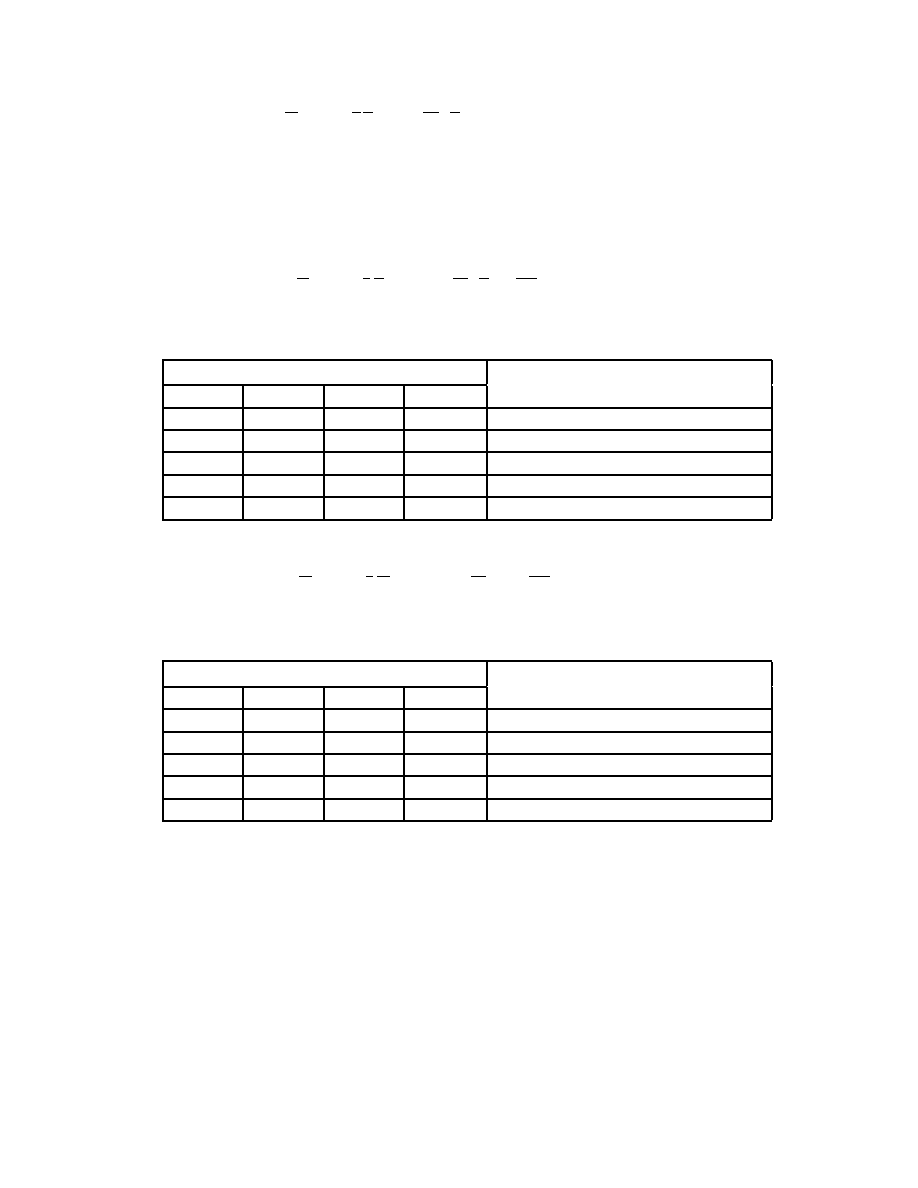
SEGA Confidential
67
SCU User's Manual
CS1 Space External Wait Effective Bit (19 [bit 12] in Figure 3.24)
A1EWT (W) A-Bus CS1 External WaiT effective bit
Wait can be entered by force by an external signal when accessing the CS1
space via the A-Bus; however, whether the process will be effective or not is
decided by this bit. A 1 shows that the process is effective, a 0 shows that the
process is ineffective. When the process is effective, wait will continue as
long as the external signal is "Low." Figure 3.29 shows differences in
timing charts when external wait is effective vs. ineffective.
CS1 space Burst Cycle Wait Number Set Bit (20~23 [bit 11~8] in Figure 3.24)
A1BW3-0 (W) A-Bus CS1 Burst cycle WaiT bit 3-0
In the CS1 space, the wait number is set for 1 cycle while a burst access is
performed. Table 3.14 shows the set values.
Table 3.14 CS1 Space Burst Cycle Set Values
CS1 Normal Cycle Wait Number Set Bit (24~27 [bit 7~4] in Figure 3.24)
A1NW3-0 (W) A-Bus CS1 Normal cycle Wait bit 3-0
In the CS1 space, the wait number is set for 1 cycle during a normal access.
Table 3.15 shows the set values.
Table 3.15 CS1 Space Normal Cycle Set Values
Bit
Wait Number
A1BW3
A1BW2
A1BW1
A1BW0
0
0
0
0
No wait (Does not sample wait)
0
0
0
1
1 cycle wait
:
:
:
:
1
1
1
0
14 cycle wait
1
1
1
1
15 cycle wait
Bit
Wait Number
A1NW3
A1NW2
A1NW1
A1NW0
0
0
0
0
No wait (Does not sample wait)
0
0
0
1
1 cycle wait
:
:
:
:
1
1
1
0
14 cycle wait
1
1
1
1
15 cycle wait
|

SEGA Confidential
68
CS1 space Burst Length Bit (28~29 [bit 3~2] in Figure 3.24)
A1LN1-0 (W) A-Bus CS1 burst LeNgth bit 1-0
The access length (boundary) is indicated while burst accessing in CS1 space.
Table 3.16 shows length values.
Table 3.16 CS1 Space Burst Length Set Values
CS1 space Bus Size Set Bit (30 [bit 0] in Figure 3.24)
A1SZ (W) A-Bus CS1 bus SiZe bit
Sets the A-Bus bus size in the CS1 space. Table 3.17 shows the set values.
Table 3.17 CS1 Space Bus Size Set Values
CS2 Space Previous Read Effective Bit (1 [bit 31] in Figure 3.25)
A2PRD (W) A-Bus CS2 Previous ReaD bit
This bit decides whether the data in the previous read process of CS2 is
effective or not. The data previous read process reduces the time from
access start until data output. This is effective only for data that is stored in
the address that follows the accessed data. Other addresses do not change
with normal addresses. A 1 shows it is effective, a 0 shows it is not effective.
See Figure 3.25 for the effect when previous read is effective.
Bit
Access Settings
A1LN1
A1LN0
0
0
No burst access
0
1
4 Address burst access
1
0
256 Address burst access
1
1
No boundary
A1SZ
Bus Size Settings
0
Indicates 16-bit bus
1
Indicates 8-bit bus
|

SEGA Confidential
69
SCU User's Manual
Bit
Access Settings
A2LN1
A2LN0
0
0
No burst access
0
1
4 Address burst access
1
0
256 Address burst access
1
1
No border
Pre-charge Insert Bit After Writing CS2 Space (2 [bit 30] in Figure 3.25)
A2WPC (W) A-Bus CS2 after Write Pre-Charge insert bit
A no-process condition of 1 clock can be inserted after writing data to CS2.
This is the bit that decides whether the process is effective or ineffective. A
1 shows it is effective, a 0 shows it is ineffective. This bit has no effect on the
operation after read. Figure 3.27 shows the operation when this bit has been
set.
Pre-charge Insert Bit After Reading CS2 Space (3 [bit 29] in Figure 3.25)
A2RPC (W) A-Bus CS2 Read Pre-Charge insert bit
A no-process condition of 1 clock can be inserted after reading data to CS2.
This is the bit that decides whether the process is effective or ineffective. A
1 shows it is effective, a 0 shows it is ineffective.This bit does not affect the
operation after write. Figure 3.28 shows the operation when this bit has
been set.
CS2 Space External Wait Effective Bit (4 [bit 28] in Figure 3.25)
A2EWT (W) A-Bus CS2 External Wait effective bit
Wait can be entered by force by an external signal when accessing the CS2
space via the A-Bus. Whether the process will be effective or not is decided by
this bit. A 1 shows that the process is effective, a 0 shows that the process is
ineffective. When the process is effective, wait will continue as long as the
external signal is "Low." Figure 3.29 shows differences in timing charts
when external wait is effective vs. ineffective.
CS2 Space Burst Length Bit (5~6 [bit 19~18] in Figure 3.25)
A2LN1-0 (W) A-Bus CS2 burst LeNgth bit 1-0
The access length (boundary) is indicated while burst accessing in CS2.
Table 3.18 shows the length settings.
Table 3.18 CS2 Space Burst Length Set Values
CS2 Bus Size Set Bit (7 [bit 16] in Figure 3.25)
A2SZ (W) A-Bus CS2 bus SiZe bit
Sets the A-Bus bus size in the CS2 space. Table 3.19 shows the set values.
|

SEGA Confidential
70
Table 3.19 CS2 Space Bus Size Set Values
Dummy Space Previous Read Effective Bit (8 [bit 15] in Figure 3.25)
A3PRD (W) A-Bus CS3 Previous ReaD bit
This bit decides whether the data previous read process of dummy space is
effective or not. The data previous read process reduces the time from access
start until data output. This is effective only for data that is stored in address
that follows the accessed data. Other addresses do not change with normal
addresses. A 1 shows it is effective, a 0 shows it is not effective. See Figure
3.26 for the result when previous read is effective.
After Pre-charge Insert Bit Dummy Space Write (9 [bit 14] in Figure 3.25)
A3WPC (W) A-Bus CS3 after Write Pre-Charge insert bit
Non-process conditions of 1 clock can be inserted after writing data to
dummy space. This is the bit that decides whether the process is effective or
ineffective. A 1 shows it is effective, a 0 shows it is ineffective. This bit hasno
effect on the operation after read. Figure 3.27 shows the operation when
this bit has been set.
After Pre-charge Insert Bit Dummy Space Read (10 [bit 13] in Figure 3.25)
A3RPC (W) A-Bus CS3 Read Pre-Charge insert bit
Non-process conditions of 1 clock can be inserted after reading data to
dummy space. This is the bit that decides whether the process is effective or
ineffective. A 1 shows it is effective, a 0 shows it is ineffective. This bit does
not affect the operation after write. Figure 3.28 shows the operation when
this bit has been set.
Dummy Space External Wait Effective Bit (11 [bit 12] in Figure 3.25)
A3EWT (W) A-Bus CS3 External WaiT effective bit
Wait can be entered by force by an external signal when accessing the
dummy space via the A-Bus. Whether the process will be effective or not is
decided by this bit. A 1 shows that the process is effective, a 0 shows that the
process is ineffective. When the process is effective, wait will continue as
long as the external signal is "Low." Figure 3.29 shows differences in
timing charts for when external wait is effective vs. when it is ineffective.
Dummy Space Burst Cycle Wait Number Set Bit (12~15 [bit 11~8] in Figure 3.25)
A3BW3-0 (W) A-Bus CS3 Burst cycle Wait bit 3-0
In dummy space, the wait number is set for 1 cycle while a burst access is
performed. Table 3.20 shows the set values.
A2SZ
Bus Size Settings
0
Indicates 16-bit bus
1
Indicates 8-bit bus
|

SEGA Confidential
71
SCU User's Manual
Table 3.20 Dummy Space Burst Cycle Set Values
Bit
Wait Number
A3BW3
A3BW2
A3BW1
A3BW0
0
0
0
0
No wait (wait not sampled)
0
0
0
1
1 cycle wait
:
:
:
:
1
1
1
0
14 cycle wait
1
1
1
1
15 cycle wait
Dummy Space Normal Cycle Wait Number Bit (16~19 [bit 7~4] in Figure 3.25)
A3NW3-0 (W) A-Bus CS 3 N ormal cycle Wait bit 3-0
In the dummy space, the wait number is set for 1 cycle during normal
accessing. Table 3.21 shows the set values.
Table 3.21 Dummy Space Normal Cycle Set Values
Bit
Wait Number
A3NW3
A3NW2
A3NW1
A3NW0
0
0
0
0
No wait (wait not sampled)
0
0
0
1
1 cycle wait
:
:
:
:
1
1
1
0
14 cycle wait
1
1
1
1
15 cycle wait
Dummy Space Burst Length Set Bit (20~21 [bit 3~2] in Figure 3.25)
A3LN1-0 (W) A-Bus CS 3 burst Le Ngth bit 1-0
In the dummy space, the length (boundary) to be accessed is designated
during burst access. Table 3.22 shows the length set values.
Table 3.22 Dummy Space Burst Length Set Values
Bit
Access Settings
A3LN1
A3LN0
0
0
No burst access
0
1
4 address burst access
1
0
256 address burst access
1
1
No boundary
|

SEGA Confidential
72
Dummy Space Bus Size Set Bit (22 [bit 0] in Figure 3.25)
A3SZ (W) A-Bus CS3 bus SiZe bit
Sets the A-Bus bus size in the dummy space. Table 3.23 shows the set values.
Table 3.23 Dummy Space Bus Size Set Values
A-Bus Refresh Register
Figure 3.30 shows the A-Bus refresh register.
1
b31
b24 b23
b16 b15
b8 b7
b0
2
3
4
5
25FE00B8
Figure 3.30 A-Bus Refresh Register (Register: AREF) Initial Value 00000000H
A-Bus Refresh Output Effective Bit (1 [bit 4] in Figure 3.30)
ARFEN (W) A-Bus ReFresh ENable bit
Makes effective the refresh cycle output of A-Bus. A 1 indicates it is effective,
a 0 indicates it is not effective.
A-Bus Refresh Wait Number Set Bit (2~5 [bit 3~0] in Figure 3.30)
ARWT3-0 (W) A-Bus Refresh WaiT bit 3-0
Sets the A-Bus refresh cycle wait number. Table 3.24 shows the details.
Table 3.24 A-Bus Refresh Wait Number
A3SZ
Bus Size Settings
0
Indicates 16 bit bus
1
Indicates 8 bit bus
Bit
Wait Number
ARWT3
ARWT2
ARWT1
ARWT0
0
0
0
0
No wait
0
0
0
1
1 cycle wait
:
:
:
:
1
1
1
0
14 cycle wait
1
1
1
1
15 cycle wait
|

SEGA Confidential
73
SCU User's Manual
3.7 SCU Control Registers
SCU SDRAM Select Register
The SCU has a register that designates the SDRAM configuration. The SDRAM
select register is shown in Figure 3.31. This register is at address 25FE00C4
H
within
the SCU.
1
b31
b24 b23
b16 b15
b8 b7
b0
25FE00C4
Figure 3.31 SCU SDRAM Select Bit (Register: RSEL) Initial Value 00000000H
SD-RAM Select Bit (1 [bit 0] in Figure 3.31)
RSEL (R/W) RAM SELect bit
RSEL=0 indicates 2 Mbit X 2
RSEL=1 indicates 4 Mbit X 2
SCU Version Register
SCU has a register showing the chip version. This register is at the address
25FE00C8
H
within the SCU. The version register is shown in Figure 3.32.
1
b31
b24 b23
b16 b15
b8 b7
b0
2
3
4
25FE00C8
Figure 3.32 SCU Version Register (Register: VER) Initial Value 00000000H
Version Number (1~4 [bit 3~0] in Figure 3.32)
VER 3-0 (R) VERsion number bit 3~0
Shows the SCU chip version. Because there are 4 bits, this supports version
0~15 chips.
|

SEGA Confidential
74
(This page is blank in the original Japanese document.)
|

SEGA Confidential
75
SCU User's Manual
CHAPTER 4 DSP CONTROL
Chapter 4 Contents
4.1
DSP Internal BLOCK MAP ................................................................76
4.2
List of Commands ................................................................................80
4.3
Operand Execution Methods .............................................................85
Jump Command Execution ...............................................85
Loop Program Execution ..................................................86
DMA Command Execution ..............................................87
End Command Execution .................................................88
4.4
Special Process Execution ...................................................................89
Loading a Program by the DMA Command ..................89
Repeating One Command .................................................89
Executing a SubRoutine Program .....................................90
4.5
More About Commands .....................................................................91
Operation Commands ........................................................91
Load Immediate Command ............................................120
DMA Command ................................................................132
Jump Commands ..............................................................141
Loop Bottom Commands .................................................153
END Command .................................................................156
|

SEGA Confidential
76
4.1
DSP Internal BLOCK MAP
Figure 4.1 (on the next page) is an internal block map of the DSP.
|

SEGA Confidential
77
SCU User's Manual
E
V
C
Z
S
T
0
PR
LE
EX
ES
E
P
DSP
PC(8)
PROGRAM RAM
(256 wordX32bit)
MDO
A (64 word X 32 bit)
W
D
RD
CT0(6)
CT1(6)
MD2
A (64 word X 32 bit)
W
D
RD
CT2(6)
CT3(6)
RA(8)
RX(32)
RY(32)
XY
MULTIPLIER
P47-0
PL(32)
PH(16)
48
BA
ACL(32)
ACH(16)
48
ALU
Q
SHIFT L16
F
E
T
C
H
TOP(8)
Instruction
decoder
Imm
TOP(12)
DS[31-0]
D0[31-0]
D0
D1
X
Y
Write address
data
read
data
MD1
A (64 word X 32 bit)
W
D
RD
MD3
A (64 word X 32 bit)
W
D
RD
Figure 4.1 Block Map Inside DSP
RA0
WA0
D
S
P external regi
st
er
|

SEGA Confidential
78
· ALU
This arithmetic unit is able to output up to 48 bits. Normal calcula-
tions are executed at 32 bits. Only product sum operations become
48-bit operations.
· MULTIPLIER
This multiplier outputs a low-order 48 bit from among the 64 bit
results obtained by 32 bit X 32 bit. The calculation results are in 48 bit
data; the high-order 16 bit is stored in PH and the low order 32 bit is
stored in PL (see below).
· TOP (W)
This is an 8 bit register that stores the lead address. The jump
command and subroutine execution process store the lead address in
this register and execute the process.
· LOP (W)
This is a 12 bit register that stores the loop counter. The number of
loops is set by the process of repeating 1 command.
· CT0-3 (W)
This is a 6 bit register that stores the access address of data RAM0-3.
· MDO-3 (R/W)
This is a 32 bit unit data port that stores the data of data
RAM0-3. There are 64 data ports in each data RAM.
· RA (W)
This is the address that stores the register for accessing the data
RAM. This register is 8 bit. The RAM designation number (0-3) is
stored by a high-order 2 bit. The RAM access address is stored by a
low-order 6 bit.
· RX (W)
This is the 32 bit X-bus connection register that stores the multiplier
input data.
· RY (W)
This is the 32 bit Y-bus connection register that stores the multiplier
input data.
· PH (W)
This register stores the high-order 16 bit within the 48 bit multiplier
output data. There is also an input data storage register that stores
the high-order 16 bit within ALU arithmetic unit input data B (48bit).
· PL (W)
This register stores the low-order 32 bit within the 48 bit of multiplier
output data. There is also an input data storage register that stores
the low-order 32 bit within ALU arithmetic unit input data B (48bit).
|

SEGA Confidential
79
SCU User's Manual
· ACH (W)
This register stores the high-order 16 bit within 48 bit data showing
the ALU calulation results. There is also an imput data storage
register that stores the high-order 16 bit within ALU arithmetic unit
input data A(48bit).
· ACL (W)
This register stores the low-order 32 bit within the 48 bit data
showing the ALU calulation results. There is also an imput data
storage register that stores the low-order 32 bit within ALU arithmetic
unit input data A(48bit).
· D0 Bus
This is a 32 bit data bus for external access. It operates at 28 MHz.
It is used in accessing the main CPU.
· X-Bus, Y-Bus
This is a 32 bit data bus for aquiring arithmetic unit input data. It
operates at 14 MHz.
· RAO (W)
This is a 32 bit external address register used in external
DSP DMA
transfer. Since it takes a 4 byte unit value, the external address should
be shifted right 2 bits.
· WAO (W)
This is a 32 bit external address register used in DSP
external DMA
transfer. Since it takes a 4 byte unit value, the external address should
be shifted right 2 bits.
|

SEGA Confidential
80
4.2
List of Commands
A list of commands used by DSP is given in Tables 4.1 to 4.4.
Table 4.1 List of Commands (1)
Type
Command
Overview of Operation
Operation Commands
ALU Control
NOP
No operation
AND
Takes the AND operation of [ACL] and [PL].
OR
Takes the OR operation of [ACL] and [PL].
XOR
Takes the exclusive OR of [ACL] and [PL].
ADD
Adds [ACL] and [PL].
SUB
Subtracts [PL] from [ACL].
AD2
Adds [ACH][ACL] and [PH][PL].
SR
Shifts [ACL] right 1 bit, stores LSB in carry flag
RR
Rotates [ACL] right 1 bit, stores LSB in carry flag
SL
Shifts [ACL] left 1 bit, stores 0 in LSB of [ACL], stores MSB
in carry flag.
RL
Rotates [ACL] left 1 bit, stores MSB in carry flag.
RL8
Rotates [ACL] left 8 bits, stores b24 in carry flag.
X-Bus Control NOP
No operation
MOV [s], X
Transfers data from data RAM to [RX]
MOV MUL, P
[MULTIPLIER] data is transfered to [PH] [PL]
MOV [s], P
Transfers data from data RAM to [PL]
Y-Bus Control NOP
No operation
MOV [s], Y
Transfers data from data RAM to [RY]
CLR A
Clears to 0 [ACH] and [ACL]
MOV ALU, A
Transfers [ALU] data to [ACH][ACL]
MOV [s], A
Transfers data from data RAM to [ACL]
D1-Bus Control
NOP
No operation
MOV SImm, [d]
SImm (short immediate) data is stored in a register or a data
RAM designated by [d].
MOV [s], [d]
Data is transfered to the RAM designated by [s] or data RAM
designated by [d] from the register.
Load Immediate
Commands
MVI Imm , [d]
Stores Imm (immediate) data in register or in data RAM
designated by [d]
MVI Imm , [d] , Z
When Z (zero flag) of the program control port is 1, Imm
(immediate) data is stored in register or in data RAM
designated by [d]
MVI Imm , [d] , NZ
When Z (zero flag) of the program control port is 0, Imm
(immediate) data is stored in register or in data RAM
designated by [d]
|

SEGA Confidential
81
SCU User's Manual
Table 4.2 List of Commands (2)
Type
Command
Overview of Operation
Load Immediate
commands
MVI Imm , [d] , S
When S (sine flag) of the program control port is 1, Imm
(immediate) data is stored in register or in data RAM
designated by [d]
MVI Imm , [d] , NS
When S (sine flag) of the program control port is 0, Imm
(immediate) data is stored in register or in data RAM
designated by [d]
MVI Imm , [d] , C
When C (carry flag) of the program control port is 1, Imm
(immediate) data is stored in register or in data RAM
designated by [d]
MVI Imm , [d] , NC
When C (carry flag) of the program control port is 0, Imm
(immediate) data is stored in register or in data RAM
designated by [d]
MVI Imm , [d] , T0
When T0 (flag while executing D0 bus DMA) of the program
control port is 1, Imm (immediate) data is stored in register or
in data RAM designated by [d]
MVI Imm , [d] , NT0
When T0 (flag while executing D0 bus DMA) of the program
control port is 0, Imm (immediate) data is stored in register or
in data RAM designated by [d]
MVI Imm , [d] , ZS
When either S (sine flag) or Z (zero flag) of the program
control port is 1, Imm (immediate) data is stored in register or
in data RAM designated by [d]
MVI Imm , [d] , NZS
When both S (sine flag) and Z (zero flag) of the program
control port are 0, Imm (immediate) data is stored in register
or in data RAM designated by [d]
DMA Commands
DMA D0, [RAM],
SImm
SImm (short immediate) data is set in the transfer word
number counter ([TN0]) as the transfer counter, and
transfers data to the RAM area designated by [RAM] from
outside using D0-Bus. Transfer begin address ([RA0]) and
transfer word number counter ([TN0]) are updated to the
value when transfer ends.
DMA [RAM], D0,
SImm
SImm (short immediate) data is set in the transfer word
number counter ([TN0]) as the transfer counter, and
transfers data from the RAM area designated by [RAM] using
D0-Bus to the outside. Transfer begin address ([WA0]) and
transfer word number counter ([TN0]) are updated to the
value when transfer ends.
|

SEGA Confidential
82
Table 4.3 List of Commands (3)
Type
Command
Overview of Operation
DMA Commands
DMA D0, [RAM], [s]
Sets data within the data RAM designated by [s] as the
transfer counter to the transfer word number counter
([TN0]), and transfers data to the RAM area designated
by [RAM] from outside using D0-Bus. Transfer begin
address ([RA0]) and transfer word number counter
([TN0]) are updated to the value when transfer ends.
DMA [RAM], D0, [s]
Sets data within the data RAM designated by [s] as the
transfer counter to the transfer word number counter
([TN0]), and transfers data to the outside from the RAM
area designated by [RAM] using D0-Bus. Transfer begin
address ([WA0]) and transfer word number counter
([TN0]) are updated to the value at the time that transfer
ends.
DMAH D0, [RAM], SImm SImm (short immediate) data is set in the transfer word
number counter ([TN0]) as the transfer counter, and
transfers data to the RAM area designated by [RAM] from
outside using D0-Bus. Transfer begin address ([RA0])
and transfer word number counter ([TN0]) keep the value
when transfer begins.
DMAH [RAM], D0, SImm SImm (short immediate) data is set as the transfer
counter in the transfer word number counter ([TN0]), and
transfers data from the RAM area designated by [RAM] to
the outside using D0-Bus. Transfer begin address
([WA0]) and transfer word number counter ([TN0]) keep
the value at the time that transfer ends.
DMAH D0, [RAM], [s]
Sets data within the data RAM designated by [s] as the
transfer counter to the transfer word number counter
([TN0]), and transfers data to the RAM area designated
by [RAM] from outside using D0-Bus. Transfer begin
address ([RA0]) and transfer word number counter
([TN0]) keep the value at the time that transfer begins.
DMAH [RAM], D0, [s]
Sets data within the data RAM designated by [s] as the
transfer counter to the transfer word number counter
([TN0]) , and transfers data to the outside from the RAM
area designated by [RAM] using D0-Bus. Transfer begin
address ([WA0]) and transfer word number counter
([TN0]) keep the value at the time that transfer begins.
JUMP Commands JMP Imm
Moves to the address shown by Imm (immediate)
JMP Z, Imm
Moves to the address shown by Imm (immediate) when
the Z (zero flag) of the program control port is 1.
JMP NZ, Imm
Moves to the address shown by Imm (immediate) when
the Z (zero flag) of the program control port is 0.
|

SEGA Confidential
83
SCU User's Manual
Table 4.4 List of Commands (4)
Type
Command
Overview of Processing
JUMP Commands JMP S, Imm
When S (sine flag) of the program control port is 1, moves to
address displayed by Imm (immediate)
JMP NS, Imm
When S (sine flag) of the program control port is 0, moves to
address displayed by Imm (immediate)
JMP C, Imm
When C (carry flag) of the program control port is 1, moves to
address displayed by Imm (immediate)
JMP NC, Imm
When C (carry flag) of the program control port is 0, moves to
address displayed by Imm (immediate)
JMP T0, Imm
When T0 (flag while executing D0 Bus DMA) of the program
control port is 1, moves to address displayed by Imm
(immediate)
JMP NT0, Imm
When T0 (flag while executing D0 Bus DMA) of the program
control port is 0, moves to address displayed by Imm
(immediate)
JMP ZS, Imm
When either Z (zero flag) or S (sine flag) of the program control
port is 1, moves to address displayed by Imm (immediate)
JMP NZS, Imm
When either Z (zero flag) or S (sine flag) of the program control
port is 0, moves to address displayed by Imm (immediate)
LOOP BOTTOM
Commands
BTM
When loop counter ([LOP]) is any number but 0, the top address
register ([TOP]) is stored in the program counter and the loop
counter ([LOP]) is decremented. No operation is done when 0.
LPS
When loop counter ([LOP]) is any number but 0, the program
counter stops, the next command is executed, loop counter
([LOP]) is decremented. This is repeated until the loop counter
is 0.
END Commands
END
Program stops and EX (program execute control flag) of the
program control port is reset.
ENDI
Program stops and EX (program execute control flag) of the
program control port is reset, and E (program end interrupt flag)
is set.
|

SEGA Confidential
84
·
Description of Constants
Follow the notation in Table 4.5.
Table 4.5 Descriptions of Constants
Notation
Description
Example
Binary
Place a "%" before numbers
%0010, %1111
Digital
Place nothing before nor after numbers
2, 10, 16, 32
Hexadecimal
Place a "$" before numbers
$05, $0A, $FF
|

SEGA Confidential
85
SCU User's Manual
4.3
Operand Execution Method
DSP controls and executes registers as shown for the following commands.
Jump Command Execution
Jump command execution is attained by storing the jump destination address (Im-
mediate Data) in the program RAM address of the program control port. But you
should be aware that commands that are pre-fetched will be executed. The condi-
tional JUMP command examines the condition of the program control port flag, and
then, if the conditions are met, stores the jump destination address in the program
RAM address of the program control port. See the section on Jump commands
under 4.5 "Commands" for the command format. Figure 4.2 is a flowchart of the
Jump command execution.
Jump
Command
Any
Conditions?
Conditions
Satisfied ?
Stores Jump destination address
in program RAM address of
program control port
Executes pre-fetched commands
END
N
Y
Y
N
Figure 4.2 Jump Command Execution
|

SEGA Confidential
86
Loop Program Execution
Execution of programs between the address designated by the top address register
([TOP]) and the BTM command of the DSP (see Loop Bottom command under 4.5
"Command" ) are repeated only the number of times indicated by the loop counter.
Thus, in order to realize this process, it must be executed after setting values in the
top address register and loop counter. Values can be set by the DSP load immediate
command (see section on Load Immediate Command under 4.5 "Command"). Ex-
ecution flow of the Loop program is shown in Figure 4.3.
Figure 4.3 Loop Program Execution
Loop End ?
([LOP]=0)
LOOP
BTM
Command ?
Sets the top address
of the Loop program
Sets number of Loops
END
Y
N
Execute command
Decrement
number of Loops
Stores the Loop program top
address in the program control port
N
Y
Execute Pre-Fetch Commands
Execute Pre-Fetch Commands
|

SEGA Confidential
87
SCU User's Manual
DMA Command Execution
This sets the DMA controller register from the DSP and explains the actual process
of DMA transfer. The DMA command is divided into the two types, shown below,
depending on the transfer direction (read / write).
1) Data transfer from the D0-Bus to the DSP.
2) Data transfer from the DSP to the D0-Bus.
· Data transfer from D0-Bus to DSP
DSP data RAM transfer begin address and external memory transfer begin
address are set in registers ([CT0-3] and [RA0]), and transfer is begun by the
DMA command. The command formats up to the DMA command are shown
below. See 4.5 "Commands" for more information.
MOV
SImm , [CT0]
; Sets DSP data RAM0 transfer begin address
MVI
Imm , [RA0]
; Sets external memory transfer begin address
DMA
D0 , [MD0] , SImm
; Begins DMA transfer using the D0 Bus
Table 4.6 is a collection of the features of DMA transfer. Because DMA transfer is
executed by 1 long word units, setting of the transfer word number (SImm of the
DMA command mentioned above) must be done in long word units.
Table 4.6 Features of Data Transfer from D0 Bus to DSP
Item
Feature
Flag Set
T0 flag of the program control port is set
Start and End
Follows the data ready signal from outside. Transfer is done by this signal in 1
long word units. DMA transfer is ended by the end signal from outside, and
the program control port T0 flag is reset by this timing.
Address Update
Each time 1 long word is transfered, 1 is added to the DSP data RAM transfer
address ([CT0-3]), and the external memory transfer address ([RA0]) is added
according to the address add number.
Hold Status
If the DMA command Hold bit (see item 4.5 "Commands" DMA command
section) is set to 1, the transfer word number ([TN0]) and external memory
transfer address ([RA0]) keep the transfer begin values.
|

SEGA Confidential
88
·
Data transfer from DSP to D0-Bus
The DSP data RAM transfer begin address and external memory begin address
are set in registers ([CT0-3]) and (WA0]), and transfer is begun by the DMA
command. The command formats up to the DMA command are shown below.
See item 4.5 for more information.
MOV
SImm , [CT0]
; Sets DSP data RAM0 transfer begin address
MVI
Imm , [WA0]
; Sets external memory transfer begin address
DMA
[MD0] , D0, SImm
; Begins DMA transfer using the D0 Bus
Table 4.7 is a collection of the features of DMA transfer. Because DMA transfer is
executed in single long word units, setting of the transfer word number (SImm of
the DMA command mentioned above) must be done in long word units.
Table 4.7 Features of Data Transfer from DSP to D0 Bus
END Command Execution
When the END command is recognized, the program control port program RAM
address add process is stopped and the program execution control bit (EX flag) is
reset. Execution of the DSP program is stopped accordingly. But data transfer by
the DMA command continues ignoring this END command until the transfer is
completed. The value of the program address when the program termintes stops at
the address that follows the address stored in END command.
Item
Feature
Flag Set
T0 flag of the program control part is set
Start and End
Obeys the data ready signal from outside. Transfer is done by this
signal in 1 long word units. DMA transfer is ended by the end signal
from outside, and the program control port T0 flag is reset by this
timing.
Address Change
Each time 1 long word is transfered, 1 is added to the DSP data RAM
transfer address ([CT0-3]), and the external memory transfer address
([WA0]) is added according to the address add number.
Hold Status
If the DMA command Hold bit (see item 4.5 "Commands" DMA
command section) is set to 1, the transfer word number ([TN0]) and
external memory transfer address ([WA0]) keep the transfer begin
values.
|

SEGA Confidential
89
SCU User's Manual
4.4
Special Process Execution
DSP can execute the following special processes.
1) Loading a Program by the DMA command
2) Repeating One Command
3) Execution of subroutine program
Loading a Program by the DMA command
Loading from the CPU was explained earlier as one method of loading a program
(see section 2.3), but a program can be loaded in the DSP program RAM by using the
DSP DMA command as well. Loading a program is done in the following formats.
MVI
Imm , [RA0]
; Sets external memory transfer begin address
DMA D0 , [PRG], SImm
; Sets transfer word number, begins transfer
MVI
Imm , [PC] , SImm
; Sets program execution start address
Repeating One Command
The format for repeating 1 command is shown below. The 1 command repeat execu-
tion command (see LPS command in section 4.5 "Command" under the part on Loop
Bottom) repeat the following commands. The repeat number executes one time
more than the set value.
MVI
Imm , [LOP]
; Sets number of repetitions
LPS
; Repeat execution comand
###
; This command is repeatedly executed
|

SEGA Confidential
90
Executing a SubRoutine Program
There are no special commands (mnemonic) in the DSP program for executing
subroutines. By combining the Load Immediate command to the [PC] with the Loop
Bottom command, subroutines are created in the form shown in Figure 4.4.
Main
Program
MOV $01 , [LOP]
MOV Imm , [PC]
NOP
Program
END
Child
Designates
execution 1 time
Sets subroutine
program start address
Caution:
Executed 2 times
Jumps after execution
Program
within subroutine
BTM
Execute pre-fetched
command of next step
Return to start address
Subroutine
Program
Figure 4.4 Subroutine Program Execution
|

SEGA Confidential
91
SCU User's Manual
4.5
More About Commands
Operation Commands
Operation commands use each X, Y, and D1 bus as well as an arithmetic logic unit
(ALU). Operation commands can be classified into the following four control types.
1) ALU control command
2) X-Bus control command
3) Y-Bus control command
4) D1-Bus control command
The operation command format is as shown in Figure 4.5.
0 0
ALU Control
X-Bus Control
Y-Bus Control
D1-Bus Control
0
13
14
19
20
25
26
30
31
29
Figure 4.5 Operation Command Format
Operation commands can execute these four types of commands concurrently.
Mnemonics should list the ALU control command to the far left. Other required
commands should be listed and separated by a space or tab.
|

SEGA Confidential
92
·
ALU Control Command
ALU control commands operate using the ALU. The following pages show more
about ALU control commands.
|

SEGA Confidential
93
SCU User's Manual
NOP
ALU No Operation
Operation
Description
No ALU command process
Label
NOP
Instruction Code
Flag
No change
Comments
0 0 0 0 0 0
0
26
b31
|

SEGA Confidential
94
AND
AND Operation
Operation
Description
Takes the AND operation of [ACL] and [PL] logical product.
Label
AND
Instruction Code
Flag
S ; 1 when operation result is negative, otherwise it is 0.
Z ; 1 when operation result is 0, otherwise it is 0.
C ; is 0.
Comments
0 0 0 0 0 1
0
26
b31
|

SEGA Confidential
95
SCU User's Manual
OR
OR Operation
Operation
Description
Takes the OR operation of [ACL] and [PL] logical sum.
Label
OR
Instruction Code
Flag
S ; 1 when operation result is negative, otherwise it is 0.
Z ; 1 when operation result is 0, otherwise it is 0.
C ; is 0.
Comments
0 0 0 0
0
1
0
26
b31
|
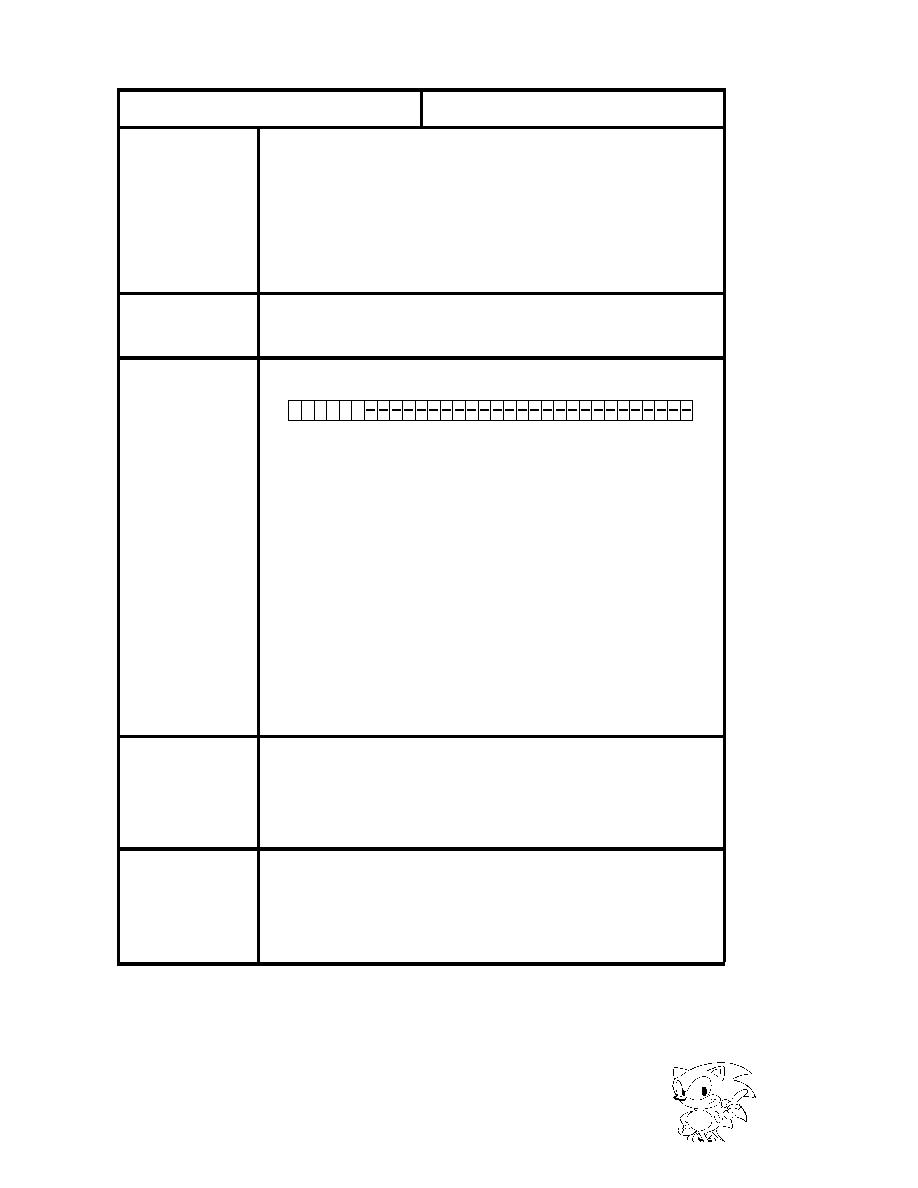
SEGA Confidential
96
XOR
Exclusive OR Operation
Operation
Description
Takes the exclusive OR operation of [ACL] and [PL].
Label
XOR
Instruction Code
Flag
S ; 1 when operation result is negative, otherwise it is 0.
Z ; 1 when operation result is 0, otherwise it is 0.
C ; this is 0.
Comments
0 0 0 0 1
0
26
b31
1
|

SEGA Confidential
97
SCU User's Manual
ADD
Addition
Operation
Description
ADDS [ACL] and [PL].
Label
ADD
Instruction Code
Flag
S ; 1 when operation result is negative, otherwise it is 0.
Z ; 1 when operation result is 0, otherwise it is 0.
C ; 1 when carry occurs as a result of the operation, otherwise it is 0.
V ; 1 when there is overflow (exceeds 48 bits)opeation result,
otherwise it is 0.
Comments
0 0 0
0
1
0
26
b31
0
|

SEGA Confidential
98
SUB
Subtraction
Operation
Description
Subtracts [PL] from [ACL].
Label
SUB
Instruction Code
Flag
S ; 1 when operation result is negative, otherwise it is 0.
Z ; 1 when operation result is 0, otherwise it is 0.
C ; 1 when carry occurs as a result of the operation, otherwise it is 0.
V ; 1 when there is underflow in the opeation result,otherwise it is 0.
Comments
0 0 0
0
1
0
26
b31
1
|

SEGA Confidential
99
SCU User's Manual
AD2
Addition
Operation
Description
Adds [ACH][ACL] and [PH][PL].
Label
AD2
Instruction Code
Flag
S ; 1 when operation result is negative, otherwise it is 0.
Z ; 1 when operation result is 0, otherwise it is 0.
C ; 1 when carry occurs as a result of the operation, otherwise it is 0.
V ; 1 when there is overflow (exceeds 48 bits)operation result,
otherwise it is 0.
Comments
0 0 0
0
1
0
26
b31
1
|

SEGA Confidential
100
SR
Right Shift 1 Bit
Operation
Description
Shifts the value of [ACL] right 1 bit, and the value of bit 0 is stored in C
flag.
Label
SR
Instruction Code
Flag
S ; 1 when operation result MSB is 1,0 when 0.
Z ; 1 when operation result is 0, otherwise it is 0.
C ; 1 when the value of b0 of input data is 1, 0 when 0.
ACL ; Shifts 1 bit to the right, most significant bit (b31) does not change
Comments
b31 b30 b29
b2
b1
b0
MSB
LSB
C
0 0
0
0
1
0
26
b31
0
|

SEGA Confidential
101
SCU User's Manual
RR
Right Rotate 1 Bit
Operation
Description
Rotates the [ACL] value right 1 bit.
Label
RR
Instruction Code
Flag
S ; 1 when operation result MSB is 1,0 when 0.
Z ; 1 when operation result is 0, otherwise it is 0.
C ; 1 when the value of b0 of input data is 1, 0 when 0.
ACL ; Shifts 1 bit to the right, least significant bit (b0) moves to the most
significant bit (b31).
Comments
b31 b30 b29
b0
MSB
LSB
C
0 0
0
1
0
26
b31
0 1
|

SEGA Confidential
102
SL
Left Shift 1 Bit
Operation
Description
Shifts the [ACL] value left 1 bit.
Label
SL
Instruction Code
Flag
S ; 1 when operation result MSB is 1,0 when 0.
Z ; 1 when operation result is 0, otherwise it is 0.
C ; 1 when the value of b31 of input data is 1, 0 when 0.
ACL ; Shifts 1 bit to the left; least significant bit (b0) is 0.
Comments
b31 b30 b29
MSB
LSB
0
C
0 0
0
1
0
26
b31
0
1
|

SEGA Confidential
103
SCU User's Manual
RL
Left Rotate 1 Bit
Operation
Description
Rotates the [ACL] value left 1 bit.
Label
RL
Instruction Code
Flag
S ; 1 when operation result MSB is 1,0 when 0.
Z ; 1 when operation result is 0, otherwise it is 0.
C ; 1 when the value of b31of input data is 1, 0 when 0.
ACL ; Shifts 1 bit to the left, most significant bit (b31) moves to the least
significant bit (b0).
Comments
b31 b30 b29
b0
MSB
LSB
C
0 0
0
1
0
26
b31
1
1
|

SEGA Confidential
104
RL8
Left Rotate 8 Bits
Operation
Description
Rotates the [ACL] value left 8 bits.
Label
RL8
Instruction Code
Flag
S ; 1 when operation result MSB is 1,0 when 0.
Z ; 1 when operation result is 0, other wise 0.
C ; 1 when the value of b24of input data is 1, 0 when 0.
ACL ; Rotates 8bits to the left.
Comments
b31 b30 b29
b0
MSB
LSB
C
0 0
1
0
26
b31
1
1
1
|

SEGA Confidential
105
SCU User's Manual
·
X-Bus Control Commands
X-Bus control commands transfer data using the X-Bus to the RX register
and PH, PL registers. The following pages show more about X-Bus control
commands.
|

SEGA Confidential
NOP
X-Bus No Operation
Operation
Description
No X-Bus control process
Label
NOP
Instruction Code
Flag
No change
Comments
0 0
0 0 0
0
25
b31
23
106
|

SEGA Confidential
MOV [s],X
Transfer (Memory
[RX])
Operation
Description
Data is transfered to [RX] from the data RAM address displayed by
[CTx(x=0~3)].
Label
MOV [Source RAM],X
Source RAM = MO ~ M3 *,MC0 ~ MC3 *
Instruction Code
Flag
* RX ; becomes data selected by multiple choice.
CTx(x=0 ~ 3) ; incremented as long as b22 = 1. No change when b22
0.
Comments
* [Mx(x=0 ~ 3)] designates DATA RAMx(x=0~3).
[MCx(x=0 ~ 3)] designates DATA RAMx(x=0~3) and after transfer,
increments [CTx(x=0~3).
[CTx]
32bit
[RX]
0 0
0 0
0
25
b31
20
1
x
x
x
Bit Data
0 0 0
0 0 1
0 1 0
0 1 1
1 0 0
1 0 1
1 1 0
1 1 1
DATA RAM0
[RX]
Process Selections
DATA RAM1
[RX]
DATA RAM2
[RX]
DATA RAM3
[RX]
DATA RAM0
[RX]
DATA RAM1
[RX]
DATA RAM2
[RX]
DATA RAM3
[RX]
,CT0++
,CT1++
,CT3++
,CT2++
bit 22 bit 21 bit 20
107
SCU User's Manual
|

SEGA Confidential
MOV MUL,P
Transfer (MULTIPLIER
[Pn])
Operation
Description
The high order 16 bit of the MULTIPLIER data 48 bit is transfered to
[PH], and the low order 32 bit is transferred to [PL]
Label
MOV MUL,P
Instruction Code
Flag
PH ; becomes MULTIPLIER high order 16 bit data
PL ; becomes the MULTIPLIER low order 32 bit data
Comments
[PH]
MULTIPLIER
16bit
32bit
[PL]
0 0
0
0
0
25
b31
20
1
108
|

SEGA Confidential
MOV [s],P
Transfer (Memory
[PL])
Operation
Description
Data is transfered to [PL] from the data RAM address displayed by
[CTx(x=0~3)]. The value of [PH] is changed by the [PL] sign
extension.
Label
MOV [Source RAM],P
Source RAM = MO ~ M3,MC0 ~ MC3 *
Instruction Code
Flag
PL ; becomes data selected by multiple choice.
PH ; changed by [PL] sign extension.
CTx(x=0~3) ; incremented when b22 = 1. No change when b22 = 0.
Comments
* [Mx(x=0 ~ 3)] designates DATA RAMx(x=0~3).
[MCx(x=0 ~ 3)] designates DATA RAMx(x=0~3) and after transfer
increments [CTx(x=0~3).
[CTx]
32bit
[PL]
0 0
0
0
25
b31
20
1 x
x
x
Bit Data
bit 22 bit 21 bit 20
0 0 0
0 0 1
0 1 0
0 1 1
1 0 0
1 0 1
1 1 0
1 1 1
DATA RAM0
[PL]
Process Selections
DATA RAM1
[PL ]
DATA RAM2
[PL]
DATA RAM3
[PL]
DATA RAM0
[PL]
DATA RAM1
[PL]
DATA RAM2
[PL]
DATA RAM3
[PL]
,CT0++
,CT1++
,CT3++
,CT2++
1
109
SCU User's Manual
|

SEGA Confidential
·
Y-Bus Control Commands
Y-Bus control commands transfer data using the Y-Bus to the RY register
and ACH, ACL registers. The following pages shows more about Y-Bus
control commands.
110
|

SEGA Confidential
NOP
Y-Bus No Operation
Operation
Description
No Y-Bus control process
Label
NOP
Instruction Code
Flag
No change
Comments
0 0
0 0 0
0
19
b31
17
111
SCU User's Manual
|

SEGA Confidential
MOV [s],Y
Transfer (Memory
[RY])
Operation
Description
Data is transfered to [RY] from the data RAM address displayed by
[CTx(x=0~3)].
Label
MOV [Source RAM],Y
Source RAM = MO ~ M3,MC0 ~ MC3 *
Instruction Code
Flag
RY ; becomes data selected by multiple choice.
CTx(x=0~3) ; incremented when b16 = 1. No change when b16 = 0.
Comments
* [Mx(x=0 ~ 3)] designates DATA RAMx(x=0~3).
[MCx(x=0 ~ 3)] designates DATA RAMx(x=0~3) and after transfer
increments [CTx(x=0~3).
[CTx]
32bit
[RY]
0 0
0
0
19
b31
14
1
x
x
x
Bit Data
bit16 bit15 bit 14
0 0 0
0 0 1
0 1 0
0 1 1
1 0 0
1 0 1
1 1 0
1 1 1
DATA RAM0
[RY]
Process Selections
DATA RAM1
[RY ]
DATA RAM2
[RY]
DATA RAM3
[RY]
DATA RAM0
[RY]
DATA RAM0
[RY]
DATA RAM0
[RY]
DATA RAM0
[RY]
,CT0++
,CT1++
,CT3++
,CT2++
0
112
|

SEGA Confidential
CLR A
0 Clear
Operation
Description
0 clears the [ACH] and [ACL] values.
Label
CLR A
Instruction Code
Flag
ACH ; becomes 0
ACL ; becomes 0
Comments
0 0
0 0 1
0
19
b31
14
113
SCU User's Manual
|

SEGA Confidential
MOV ALU,A
Transfer ([ALU]
[ACH][ACL])
Operation
Description
Transfers the value of the [ALU] high order 16 bit to [ACH] and the
value of the [ALU] low order 32 bit to [ACL].
Label
MOV ALU,A
Instruction Code
Flag
ACH ; becomes ALU high order 16 bit data
ACL ; becomes ALU low order 32 bit data
Comments
[ACH]
ALU
16bit
32bit
[ACL]
0 0
0
0
1
0
19
b31
14
114
|

SEGA Confidential
MOV [s],A
Transfer (Memory
[ACL])
Operation
Description
Data is transfered to [ACL] from the data RAM address displayed by
[CTx(x=0~3)]. The value of [ACH] is changed by the sign extension of
[ACL].
Label
MOV [Source RAM],A
Source RAM = MO ~ M3,MC0 ~ MC3 *
Instruction Code
Flag
ACL ; becomes data selected by multiple choice.
ACH ; is changed by the sign extension of [ACL]
CTx(x=0~3) ; incremented when b16 = 1. No change when b16 = 0.
Comments
* [Mx(x=0 ~ 3)] designates DATA RAMx(x=0~3).
[MCx(x=0 ~ 3)] designates DATA RAMx(x=0~3) and after transfer
increments [CTx(x=0~3).
[CTx]
32bit
[ACL]
0 0
0
19
b31
14
1
x
x
x
Bit Data
bit16 bit15 bit 14
0 0 0
0 0 1
0 1 0
0 1 1
1 0 0
1 0 1
1 1 0
1 1 1
DATA RAM0
[ACL]
Process Selections
DATA RAM1
[ACL]
DATA RAM2
[ACL]
DATA RAM3
[ACL]
DATA RAM0
[ACL]
DATA RAM1
[ACL]
DATA RAM2
[ACL]
DATA RAM3
[ACL]
,CT0++
,CT1++
,CT3++
,CT2++
0
1
115
SCU User's Manual
|

SEGA Confidential
·
D1-Bus Control Commands
D1-Bus control commands control the exchange of data between memory
connected to the D1-Bus. The following pages shows more about D1-Bus
control commands.
116
|

SEGA Confidential
NOP
D1-Bus No Operation
Operation
Description
No D1-Bus control process
Label
NOP
Instruction Code
Flag
No change
Comments
0 0
0 0
0
b31
13
117
SCU User's Manual
|

SEGA Confidential
MOV SImm,[d]
Transfer (SImm
[destination])
Operation
Description
SImm data is transfered to the RAM or register designated by
[destination]. SImm data is signed 8 bit data.
Label
MOV SImm,[Destination]
Destination = MC0 ~ MC3 *,RX,PL,RA0,WA0,LOP,TOP,CT0 ~ CT3
Instruction Code
Flag
Area selected by [d] selection ; becomes Imm data
Comments
* [MCx(x=0 ~ 3)] designates DATA RAMx(x=0~3) and, after transfer,
increments [CTx(x=0~3).
[destination]
D31 - 7
b7
D6-0
b6-0
Short Immediate Data
0 0
0
b31
13
1 x
x
x
0
x
8 7
Bit Data
bit11 bit10 bit 9
DATA RAM0
[d] Selections
DATA RAM1
DATA RAM2
DATA RAM3
,CT0++
,CT1++
,CT3++
,CT2++
0
0
0
0
0
0
0
0
1
1
1
1
1
1
1
1
0
0
0
0
1
1
1
1
0
0
0
0
1
1
1
1
0
0
1
1
0
0
1
1
0
0
1
1
0
0
1
1
0
1
0
1
0
1
0
1
0
1
0
1
0
1
0
1
bit 8
[RX]
[PL]
[RA0]
[WA0]
unused
unused
[LOP]
[TOP]
[CT0]
[CT1]
[CT2]
[CT3]
SImm Data
118
|

SEGA Confidential
MOV [s],[d]
Transfer ([source]
[destination])
Operation
Description
RAM data or register data designated by [source] is transfered to the
RAM or register designated by [destination].
Label
MOV [Source], [Destination]
Source = M0 ~ M3 *,MC0 ~ MC3 *,ALH,ALL
Destination = MC0 ~ MC3,RX,PL,RA0,WA0,LOP,TOP,CT0 ~ CT3
Instruction Code
Flag
Area selected by [d] selection is data of an area selected by [s] selectio
Comments
* [Mx(x=0 ~ 3)] designates DATA RAM x(x=0~3)
[MCx(x=0 ~ 3)] designates DATA RAM x(x=0~3) and, after transfer,
increments [CTx(x=0~3).
0 0
0
b31
13
1 x
x
x
8
3
1
x
x
x
x
x
DATA RAM0
[s] Selections
DATA RAM1
DATA RAM2
DATA RAM3
DATA RAM0
DATA RAM1
DATA RAM2
DATA RAM3
,CT0++
,CT1++
,CT3++
,CT2++
Bit Data
0
0
0
0
0
0
0
0
1
1
1
no field
[ALU LOW]
[ALU HIGH]
0
0
0
0
1
1
1
1
0
0
0
0
0
1
1
0
0
1
1
0
0
1
0
1
0
1
0
1
0
1
0
1
0
bit 3 bit 2 bit 1 bit 0
Bit Data
bit11 bit10 bit 9
DATA RAM0
[d] Selections
DATA RAM1
DATA RAM2
DATA RAM3
,CT0++
,CT1++
,CT3++
,CT2++
0
0
0
0
0
0
0
0
1
1
1
1
1
1
1
1
0
0
0
0
1
1
1
1
0
0
0
0
1
1
1
1
0
0
1
1
0
0
1
1
0
0
1
1
0
0
1
1
0
1
0
1
0
1
0
1
0
1
0
1
0
1
0
1
bit 8
[RX]
[PL]
[RA0]
[WA0]
unused
unused
[LOP]
[TOP]
[CT0]
[CT1]
[CT2]
[CT3]
119
SCU User's Manual
|

SEGA Confidential
Load Immediate Command
The load immediate command transfers immediate data to the storage destination.
Unconditional transfer follows the format in Figure 4.6. Conditional transfer follows
the format in Figure 4.7. Details are on the following pages.
1 0
Storage
Destination
0
Immediate data
31 30 29
26 25 24
0
Figure 4.6 Load Immediate Command Format 1 (Unconditional Transfer)
1 0
Storage
Destination
1
Immediate data
31 30 29
26 25 24
0
Status
19 18
Figure 4.7 Load Immediate Command Format 2 (Conditional Transfer)
120
|

SEGA Confidential
MVI Imm,[d]
Unconditional Transfer (Imm
[destination])
Operation
Description
Imm data is unconditional and is transfered to the RAM or register
designated by [destination].
Imm data is signed 25 bit data.
Label
MVI Imm,[Destination]
Destination = MC0 ~ MC3 *,RX,PL,RA0,WA0,LOP,PC
Instruction Code
Flag
Area selected by [d] multiple choice ; becomes Imm data
Comments
* [MCx(x=0 ~ 3)] designates DATA RAM x(x=0~3) and, after transfer,
increments [CTx(x=0~3).
0
0
b31
x
x
x
x
Bit Data
bit11 bit10 bit 9
DATA RAM0
[d] Selections
DATA RAM1
DATA RAM2
DATA RAM3
,CT0++
,CT1++
,CT3++
,CT2++
0
0
0
0
0
0
0
0
1
1
1
1
1
1
1
1
0
0
0
0
1
1
1
1
0
0
0
0
1
1
1
1
0
0
1
1
0
0
1
1
0
0
1
1
0
0
1
1
0
1
0
1
0
1
0
1
0
1
0
1
0
1
0
1
bit 8
[RX]
[PL]
[RA0]
[WA0]
unused
unused
[LOP]
[PC] [TOP] ,[PC]
Imm Data
1
0
unused
unused
unused
unused
24
121
SCU User's Manual
|

SEGA Confidential
MVI Imm,[d]Z
Conditional Transfer (Z=1 then Imm
[destination])
Operation
Description
When the Z flag is 1, Imm data is transfered to the RAM or register
designated by [destination]. Imm data is signed 19 bit data.
Can be used as execution of the subroutine program (see instruction
code**) by sending Imm data (subtroutine begin dress) to the PC and
saving the PC (jump address after subroutine ends) value to TOP. Be
aware that the address next after this command will be executed twice
once before the subroutine and once after.
Label
MVI Imm,[Destination],Z
Destination RAM = MC0 ~ MC3 *,RX,PL,RA0,WA0,LOP,PC
Instruction Code
Flag
Area selected by [d] selection ; becomes Imm data
Comments
* [MCx(x=0 ~ 3)] designates DATA RAM x(x=0~3) and, after transfer,
increments [CTx(x=0~3).
0
0
b31
x
x
x
x
Bit Data
bit29 bit28 bit27 bit26
DATA RAM0
[d] Selections
DATA RAM1
DATA RAM2
DATA RAM3
,CT0++
,CT1++
,CT3++
,CT2++
0
0
0
0
0
0
0
0
1
1
1
1
1
1
1
1
0
0
0
0
1
1
1
1
0
0
0
0
1
1
1
1
0
0
1
1
0
0
1
1
0
0
1
1
0
0
1
1
0
1
0
1
0
1
0
1
0
1
0
1
0
1
0
1
[RX]
[PL]
[RA0]
[WA0]
unused
unused
[LOP]
[PC] [TOP] ,[PC]
Imm Data
1
unused
unused
unused
unused
18
1 1
1
0 0 0 0
122
|

SEGA Confidential
MVI =Imm,[d]NZ
Conditional Transfer (Z=0 then Imm
[destination])
Operation
Description
When the Z flag is 0, Imm data is transfered to the RAM or register
designated by [destination]. Imm data is signed 19 bit data.
Can be used as execution of the subroutine program (see instruction
code**) by sending Imm data (subtroutine begin dress) to the PC and
saving the PC (jump address after subroutine ends) value to TOP. Be
aware that the address next after this command will be executed twice
once before the subroutine and once after.
Label
MVI Imm,[Destination],NZ
Destination = MC0 ~ MC3 *,RX,PL,RA0,WA0,LOP,PC
Instruction Code
Flag
Area selected by [d] selection ; becomes Imm data
Comments
* [MCx(x=0 ~ 3)] designates DATA RAM x(x=0~3) and, after transfer ,
increments [CTx(x=0~3).
0
0
b31
x
x
x
x
Bit Data
bit29 bit28 bit27 bit26
DATA RAM0
[d] Selections
DATA RAM1
DATA RAM2
DATA RAM3
,CT0++
,CT1++
,CT3++
,CT2++
0
0
0
0
0
0
0
0
1
1
1
1
1
1
1
1
0
0
0
0
1
1
1
1
0
0
0
0
1
1
1
1
0
0
1
1
0
0
1
1
0
0
1
1
0
0
1
1
0
1
0
1
0
1
0
1
0
1
0
1
0
1
0
1
[RX]
[PL]
[RA0]
[WA0]
unused
unused
[LOP]
[PC] [TOP] ,[PC]
Imm Data
1
unused
unused
unused
unused
18
1 1
1
0 0 0 0
123
SCU User's Manual
|
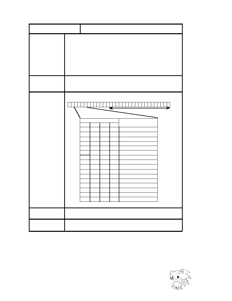
SEGA Confidential
MVI Imm,[d]S
Conditional Transfer (S=1 then Imm
[destination])
Operation
Description
When the S flag is 1, Imm data is transfered to the RAM or register
designated by [destination]. Imm data is signed 19 bit data.
Can be used asexecution of the subroutine program (see instruction
code**) by sending Imm data (subtroutine begin dress) to the PC and
saving the PC (jump address after subroutine ends) value to TOP. Th
address next after this command will be executed twice, once before
the subroutine and once after.
Label
MVI Imm,[Destination],S
Destination = MC0 ~ MC3 *,RX,PL,RA0,WA0,LOP,PC
Instruction Code
Flag
Area selected by [d] selection ; becomes Imm data
Comments
* [MCx(x=0 ~ 3)] designates DATA RAM x(x=0~3) and, after transfer,
increments [CTx(x=0~3).
0
0
b31
x
x
x
x
Bit Data
bit29 bit28 bit27 bit26
DATA RAM0
[d] Selections
DATA RAM1
DATA RAM2
DATA RAM3
,CT0++
,CT1++
,CT3++
,CT2++
0
0
0
0
0
0
0
0
1
1
1
1
1
1
1
1
0
0
0
0
1
1
1
1
0
0
0
0
1
1
1
1
0
0
1
1
0
0
1
1
0
0
1
1
0
0
1
1
0
1
0
1
0
1
0
1
0
1
0
1
0
1
0
1
[RX]
[PL]
[RA0]
[WA0]
unused
unused
[LOP]
[PC] [TOP] ,[PC]
Imm Data
1
unused
unused
unused
unused
18
1 1
1
0 0 0
0
124
|

SEGA Confidential
MVI Imm,[d]NS
Conditional Transfer (S=0 then Imm
[destination])
Operation
Description
When the S flag is 0, Imm data is transfered to the RAM or register
designated by [destination]. Imm data is signed 19 bit data.
Can be used asexecution of the subroutine program (see instruction
code**) by sending Imm data (subtroutine begin dress) to the PC and
saving the PC (jump address after subroutine ends) value to TOP. Be
aware that the address next after this command will be executed twice
once before the subroutine and once after.
Label
MVI Imm,[Destination],NS
Destination = MC0 ~ MC3 *,RX,PL,RA0,WA0,LOP,PC
Instruction Code
Flag
Area selected by [d] selection ; becomes Imm data
Comments
* [MCx(x=0 ~ 3)] designates DATA RAM x(x=0~3) and, after transfer,
increments [CTx(x=0~3).
0
0
b31
x
x
x
x
Bit Data
bit29 bit28 bit27 bit26
DATA RAM0
[d] Selections
DATA RAM1
DATA RAM2
DATA RAM3
,CT0++
,CT1++
,CT3++
,CT2++
0
0
0
0
0
0
0
0
1
1
1
1
1
1
1
1
0
0
0
0
1
1
1
1
0
0
0
0
1
1
1
1
0
0
1
1
0
0
1
1
0
0
1
1
0
0
1
1
0
1
0
1
0
1
0
1
0
1
0
1
0
1
0
1
[RX]
[PL]
[RA0]
[WA0]
unused
unused
[LOP]
[PC] [TOP] ,[PC]
Imm Data
1
unused
unused
unused
unused
18
1 1
1
0 0 0
0
125
SCU User's Manual
|

SEGA Confidential
MVI Imm,[d]C
Conditional Transfer (C=1 then Imm
[destination])
Operation
Description
When the C flag is 1, Imm data is transfered to the RAM or register
designated by [destination]. Imm data is signed 19 bit data.
Can be used asexecution of the subroutine program (see instruction
code**) by sending Imm data (subtroutine begin dress) to the PC and
saving the PC (jump address after subroutine ends) value to TOP. Be
aware that the address next after this command will be executed twice
once before the subroutine and once after.
Label
MVI Imm,[Destination],C
Destination = MC0 ~ MC3 *,RX,PL,RA0,WA0,LOP,PC
Instruction Code
Flag
Area selected by [d] selection ; becomes Imm data
Comments
* [MCx(x=0 ~ 3)] designates DATA RAM x(x=0~3) and, after transfer,
increments [CTx(x=0~3).
0
0
b31
x
x
x
x
Bit Data
bit29 bit28 bit27 bit26
DATA RAM0
[d] Selections
DATA RAM1
DATA RAM2
DATA RAM3
,CT0++
,CT1++
,CT3++
,CT2++
0
0
0
0
0
0
0
0
1
1
1
1
1
1
1
1
0
0
0
0
1
1
1
1
0
0
0
0
1
1
1
1
0
0
1
1
0
0
1
1
0
0
1
1
0
0
1
1
0
1
0
1
0
1
0
1
0
1
0
1
0
1
0
1
[RX]
[PL]
[RA0]
[WA0]
unused
unused
[LOP]
[PC] [TOP] ,[PC]
Imm Data
1
unused
unused
unused
unused
18
1 1
1
0 0
0 0
126
|

SEGA Confidential
MVI Imm,[d]NC
Conditional Transfer (C=0 then Imm
[destination])
Operation
Description
When the C flag is 0, Imm data is transfered to the RAM or register
designated by [destination]. Imm data is signed 19 bit data.
Can be used asexecution of the subroutine program (see instruction
code**) by sending Imm data (subtroutine begin dress) to the PC and
saving the PC (jump address after subroutine ends) value to TOP. Be
aware that the address next after this command will be executed twice
once before the subroutine and once after.
Label
MVI Imm,[Destination],NC
Destination = MC0 ~ MC3 *,RX,PL,RA0,WA0,LOP,PC
Instruction Code
Flag
Area selected by [d] selection ; becomes Imm data
Comments
* [MCx(x=0 ~ 3)] designates DATA RAM x(x=0~3) and, after transfer,
increments [CTx(x=0~3).
0
0
b31
x
x
x
x
Bit Data
bit29 bit28 bit27 bit26
DATA RAM0
[d] Selections
DATA RAM1
DATA RAM2
DATA RAM3
,CT0++
,CT1++
,CT3++
,CT2++
0
0
0
0
0
0
0
0
1
1
1
1
1
1
1
1
0
0
0
0
1
1
1
1
0
0
0
0
1
1
1
1
0
0
1
1
0
0
1
1
0
0
1
1
0
0
1
1
0
1
0
1
0
1
0
1
0
1
0
1
0
1
0
1
[RX]
[PL]
[RA0]
[WA0]
unused
unused
[LOP]
[PC] [TOP] ,[PC]
Imm Data
1
unused
unused
unused
unused
18
1 1
1
0 0
0 0
127
SCU User's Manual
|

SEGA Confidential
MVI Imm,[d],T0
Conditional Transfer (T0=1 then Imm
[destination])
Operation
Description
When the T0 flag is 1, Imm data is transfered to the RAM or register
designated by [destination]. Imm data is signed 19 bit data.
Can be used asexecution of the subroutine program (see instruction
code**) by sending Imm data (subtroutine begin dress) to the PC and
saving the PC (jump address after subroutine ends) value to TOP. Be
aware that the address next after this command will be executed twice
once before the subroutine and once after.
Label
MVI Imm,[Destination],T0
Destination = MC0 ~ MC3 *,RX,PL,RA0,WA0,LOP,PC
Instruction Code
Flag
Area selected by [d] selection ; becomes Imm data
Comments
* [MCx(x=0 ~ 3)] designates DATA RAM x(x=0~3) and, after transfer,
increments [CTx(x=0~3).
0
0
b31
x
x
x
x
Bit Data
bit29 bit28 bit27 bit26
DATA RAM0
[d] Selections
DATA RAM1
DATA RAM2
DATA RAM3
,CT0++
,CT1++
,CT3++
,CT2++
0
0
0
0
0
0
0
0
1
1
1
1
1
1
1
1
0
0
0
0
1
1
1
1
0
0
0
0
1
1
1
1
0
0
1
1
0
0
1
1
0
0
1
1
0
0
1
1
0
1
0
1
0
1
0
1
0
1
0
1
0
1
0
1
[RX]
[PL]
[RA0]
[WA0]
unused
unused
[LOP]
[PC] [TOP] ,[PC]
Imm Data
1
unused
unused
unused
unused
18
1 1
1
0
0
0
0
128
|

SEGA Confidential
MVI Imm,[d]NT0
Conditional Transfer (T0=0 then Imm
[destination])
Operation
Description
When the T0 flag is 0, Imm data is transfered to the RAM or register
designated by [destination]. Imm data is signed 19 bit data.
Can be used asexecution of the subroutine program (see instruction
code**) by sending Imm data (subtroutine begin dress) to the PC and
saving the PC (jump address after subroutine ends) value to TOP. Be
aware that the address next after this command will be executed twice
once before the subroutine and once after.
Label
MVI Imm,[Destination],NT0
Destination = MC0 ~ MC3 *,RX,PL,RA0,WA0,LOP,PC
Instruction Code
Flag
Area selected by [d] selection ; becomes Imm data
Comments
* [MCx(x=0 ~ 3)] designates DATA RAM x(x=0~3) and, after transfer,
increments [CTx(x=0~3).
0
0
b31
x
x
x
x
Bit Data
bit29 bit28 bit27 bit26
DATA RAM0
[d] Selections
DATA RAM1
DATA RAM2
DATA RAM3
,CT0++
,CT1++
,CT3++
,CT2++
0
0
0
0
0
0
0
0
1
1
1
1
1
1
1
1
0
0
0
0
1
1
1
1
0
0
0
0
1
1
1
1
0
0
1
1
0
0
1
1
0
0
1
1
0
0
1
1
0
1
0
1
0
1
0
1
0
1
0
1
0
1
0
1
[RX]
[PL]
[RA0]
[WA0]
unused
unused
[LOP]
[PC] [TOP] ,[PC]
Imm Data
1
unused
unused
unused
unused
18
1
1
0
0 0 0
0
129
SCU User's Manual
|

SEGA Confidential
MVI Imm,[d]ZS
Conditional Transfer (Z=1 or S=1 then Imm
[destination])
Operation
Description
When the Z flag or S flag is 1, Imm data is transfered to the RAM or
register designated by [destination]. Imm data is signed 19 bit data.
Can be used asexecution of the subroutine program (see instruction
code**) by sending Imm data (subtroutine begin dress) to the PC and
saving the PC (jump address after subroutine ends) value to TOP. Be
aware that the address next after this command will be executed twice
once before the subroutine and once after.
Label
MVI Imm,[Destination],ZS
Destination = MC0 ~ MC3 *,RX,PL,RA0,WA0,LOP,PC
Instruction Code
Flag
Area selected by [d] selection ; becomes Imm data
Comments
* [MCx(x=0 ~ 3)] designates DATA RAM x(x=0~3) and, after transfer,
increments [CTx(x=0~3).
0
0
b31
x
x
x
x
Bit Data
bit29 bit28 bit27 bit26
DATA RAM0
[d] Selections
DATA RAM1
DATA RAM2
DATA RAM3
,CT0++
,CT1++
,CT3++
,CT2++
0
0
0
0
0
0
0
0
1
1
1
1
1
1
1
1
0
0
0
0
1
1
1
1
0
0
0
0
1
1
1
1
0
0
1
1
0
0
1
1
0
0
1
1
0
0
1
1
0
1
0
1
0
1
0
1
0
1
0
1
0
1
0
1
[RX]
[PL]
[RA0]
[WA0]
unused
unused
[LOP]
[PC] [TOP] ,[PC]
Imm Data
1
unused
unused
unused
unused
18
1 1 0
0
0
1 1
130
|

SEGA Confidential
MVI Imm,[d]NZS
Conditional Transfer (Z=0=S then Imm
[destination])
Operation
Description
When the Z flag or S flag are both 0, Imm data is transfered to the RA
or register designated by [destination]. Imm data is signed 19 bit data
Can be used as execution of the subroutine program (see instruction
code**) by sending Imm data (subtroutine begin dress) to the PC and
saving the PC (jump address after subroutine ends) value to TOP. Be
aware that the address next after this command will be executed twice
once before the subroutine and once after.
Label
MVI Imm,[Destination],NZS
Destination = MC0 ~ MC3 *,RX,PL,RA0,WA0,LOP,PC
Instruction Code
Flag
Area selected by [d] selection ; becomes Imm data
Comments
* [MCx(x=0 ~ 3)] designates DATA RAM x(x=0~3) and, after transfer,
increments [CTx(x=0~3).
0
0
b31
x
x
x
x
Bit Data
bit29 bit28 bit27 bit26
DATA RAM0
[d] Selections
DATA RAM1
DATA RAM2
DATA RAM3
,CT0++
,CT1++
,CT3++
,CT2++
0
0
0
0
0
0
0
0
1
1
1
1
1
1
1
1
0
0
0
0
1
1
1
1
0
0
0
0
1
1
1
1
0
0
1
1
0
0
1
1
0
0
1
1
0
0
1
1
0
1
0
1
0
1
0
1
0
1
0
1
0
1
0
1
[RX]
[PL]
[RA0]
[WA0]
unused
unused
[LOP]
[PC] [TOP] ,[PC]
Imm Data
1
unused
unused
unused
unused
18
1
0
0
0
1 1
0
131
SCU User's Manual
|

SEGA Confidential
DMA Command
DMA commands transfer data of an external and DSP internal RAM through an
external bus. There are two methods, one of which is setting the transfer word
number directly by Imm data, and the other is setting the internal RAM transfer
word number by designating the number of the internal data RAM. The first
method is shown in Figure 4.8 and the second method is shown in Figure 4.9.
Details of the command are shown on the pages that follow.
1
0 0
Immediate data
31 30 29 28 27
0
1
RAM
H
0
dir
Add
Mode
18 17 15 14 13 12 11 10 8 7
Figure 4.8 DMA Command Format 1
1
0 0
SOURCE
31 30 29 28 27
0
1
RAM
H
1
dir
Add
Mode
18 17 15 14 13 12 11 10 8 7
3 2
Figure 4.9 DMA Command Format 2
132
|

SEGA Confidential
DMA D0,[RAM],SImm
DMA Transfer (D0[31-0]
RAM)
Operation
Description
D0[31-0] data is transfered to RAM . The external address register
and transfer word number register are updated (added) according to
the address add number. The transfer word number register is a
register for storing the transfer word number in long word units. This
word number is either 0 or transfer ends when forced to end.
Label
DMA D0,[Destination],Counter
Destination = M0 ~ M3 *
Instruction Code
Flag
T0 ; becomes 1.
Comments
* [MCx(x=0 ~ 3)] selects DATA RAM x(x=0~3).
**When the END signal informing you that transfer end from outside
has been entered, T0; becomes 0.
Designating address-add adds an add number after the command and
becomes DMA0~DMA64.
Add number is1 when address add number designation is omitted.
The transfer source address is set in advance to RA0 and the transfer
destination RAM address is set in advance to CTx.
0
0
b31
x
x
x
x
Bit Data
bit17 bit16 bit15
Address Add 0
Add Mode Selections
0
0
0
0
1
1
1
1
0
0
1
1
0
0
1
1
0
1
0
1
0
1
0
1
SImm Data
1
17
1
0
0
0 0
0
0
15
7
x
Address Add 1
Address Add 2
Address Add 4
Address Add 8
Address Add 16
Address Add 32
Address Add 64
Bit Data
bit9 bit8
Selections
0
0
1
1
0
1
0
1
DATA RAM 0
DATA RAM 1
DATA RAM 2
DATA RAM 3
28
133
SCU User's Manual
|

SEGA Confidential
DMA [RAM],D0,SImm
DMA Transfer (RAM
D0[31-0])
Operation
Description
RAM data is transfered to D0[31-0]. The external address register and
transfer word number register are updated (added) according to the
address add number. Only add numbers 0 and 1 are valid for the A
-
Bus and the write unit is 32bit. All add numbers (0 - 64) are valid for
the B-Bus. Write unit is16bit; 32bit data is divided in half and written at
intervals of16X (0-64). The transfer word number register is a register
for storing the transfer word number in long word units. This word
number is either 0 or transfer ends when forced to end.
Label
DMA [Source],D0,Counter
Source = Mo ~ M3 *
Instruction Code
Flag
T0 ; becomes 1.
Comments
* [MCx(x=0 ~ 3)] selects DATA RAM x(x=0~3).
**When the END signal informing you that transfer end from outside
has been entered, T0; becomes 0.
Designating address-add adds an add number after the command and
becomes DMA0~DMA64.
Add number is 1 when address add number designation is omitted.
The transfer source RAM address is set in advance to CTx and the
transfer destination address is set in advance to WA0.
0
0
b31
x
x
x
x
Bit Data
bit17 bit16 bit15
Address Add 0
Add Mode Selections
0
0
0
0
1
1
1
1
0
0
1
1
0
0
1
1
0
1
0
1
0
1
0
1
SImm Data
1
17
1
0
0
0 1
0
0
15
7
x
Address Add 1
Address Add 2
Address Add 4
Address Add 8
Address Add 16
Address Add 32
Address Add 64
Bit Data
bit9 bit8
Selections
0
0
1
1
0
1
0
1
DATA RAM 0
DATA RAM 1
DATA RAM 2
DATA RAM 3
134
|

SEGA Confidential
DMA D0,[RAM],[s]
DMA Transfer (D0[31-0]
RAM
)
Operation
Description
[s] data designated by bit0~2 is treated as a transfer counter, and only
numbers displayed transfer D0[31-0] data to the RAM. External
address register and transfer word number register are updated
(added) according to the address add number. The transfer word
number register stores transfer word numbers in long word units. This
word number becomes 0 or transfer ends when forced to end.
Label
DMA D0,[Destination],[Counter]
Counter = M0 ~ M3 *,MC0~MC3*
Destination = M0~M3 *,PRG *
Instruction
Code
Valid only for A-Bus
Address add is 32bit units.
Flag
T0 ; becomes 1. **
CTx(x0~3) ; incremented when b2=1. When b2=0, there is no change
Comments
* [MCx(x=0 ~ 3)] selects DATA RAM x(x=0~3). MCx(x=0~3) selects
DATA RAM x(x=0~3), and after transfer increments CTx(x0~3).
PRG selects program RAM.
**When the END signal informing you that transfer end from outside
has been entered, T0; becomes 0.
Designating address-add adds an add number after the command an
becomes DMA0~DMA1.
Add number is 1 when address add number designation is omitted.
The transfer source address is set in advance to RA0 and the transfer
destination RAM address is set in advance to CTx.
0
0
b31
x
x
Bit Data
bit 2 bit1 bit 0
[s] Selections
0
0
0
0
1
1
1
1
0
0
1
1
0
0
1
1
0
1
0
1
0
1
0
1
1 1
0
0 1
0
0
7
x
Bit Data
bit9 bit8
RAM Selections
0
0
1
1
0
1
0
1
DATA RAM 0
DATA RAM 1
DATA RAM 2
DATA RAM 3
DATA RAM 0
DATA RAM 1
DATA RAM 2
DATA RAM 3
DATA RAM 0
DATA RAM 1
DATA RAM 2
DATA RAM 3
,CT0++
,CT1++
,CT2++
,CT3++
x
x
x
x
0 0
28
0
0
0
0
bit 10
0
0
PROGRAM RAM
1
Add Mode Selections
Address Add 0
Address Add 1
bit 15
0
1
135
SCU User's Manual
|

SEGA Confidential
DMA [RAM],D0,[s]
DMA Transfer (RAM
D0[31-0]
)
Operation
Description
[s] data designated by bit0~2 is treated as a transfer counter, and only
numbers displayed transfer RAM data to DO[31-0] data. External
address register and transfer word number register are updated
(added) according to the address add number. The transfer word
number register stores transfer word numbers in long word units. But
only add numbers 0 and 1 are valid for A-Bus, and write units are 32
bits. For B-Bus, all add numbers (0-64) are valid. Write units are 16 bit;
32 bit data is divided in half and written at intervals of 16bitX (0-64). Th
transfer word number register stores transfer words in long word units.
This word number becomes 0 or transfer ends when forced to end.
Label
DMA D0,[Destination],[Counter]
Counter = M0 ~ M3 *,MC0~MC3*
Source = M0~M3 *,PR*
Instruction
Code
Flag
T0 ; becomes 1. **
CTx(x=0~3) ; incremented when b2=1. No changes when b2=0.
Comments
* [MCx(x=0 ~ 3)] selects DATA RAM x(x=0~3). MCx(x=0~3) selects
DATA RAM x(x=0~3), and after transfer increments CTx(x0~3).
**When the END signal informing you that transfer end from outside
has been entered, T0; becomes 0.
Designating address-add adds an add number after the command an
becomes DMA0~DMA64.
Add number is 1 when address add number designation is omitted.
The transfer source RAM address is set in advance to CTx and the
transfer destination address is set in advance to WA0.
0
0
b31
x
x
x
x
Bit Data
bit17 bit16 bit15
Address Add 0
Add Mode Selections
0
0
0
0
1
1
1
1
0
0
1
1
0
0
1
1
0
1
0
1
0
1
0
1
1
17
1
0
0
1
0
0
7
x
Address Add 1
Address Add 2
Address Add 4
Address Add 8
Address Add 16
Address Add 32
Address Add 64
Bit Data
bit9 bit8
RAM Selections
0
0
1
1
0
1
0
1
DATA RAM 0
DATA RAM 1
DATA RAM 2
DATA RAM 3
1
x
x
x
Bit Data
bit 2 bit1 bit 0
[s] Selections
0
0
0
0
1
1
1
1
0
0
1
1
0
0
1
1
0
1
0
1
0
1
0
1
DATA RAM 0
DATA RAM 1
DATA RAM 2
DATA RAM 3
DATA RAM 0
DATA RAM 1
DATA RAM 2
DATA RAM 3
,CT0++
,CT1++
,CT2++
,CT3++
136
|
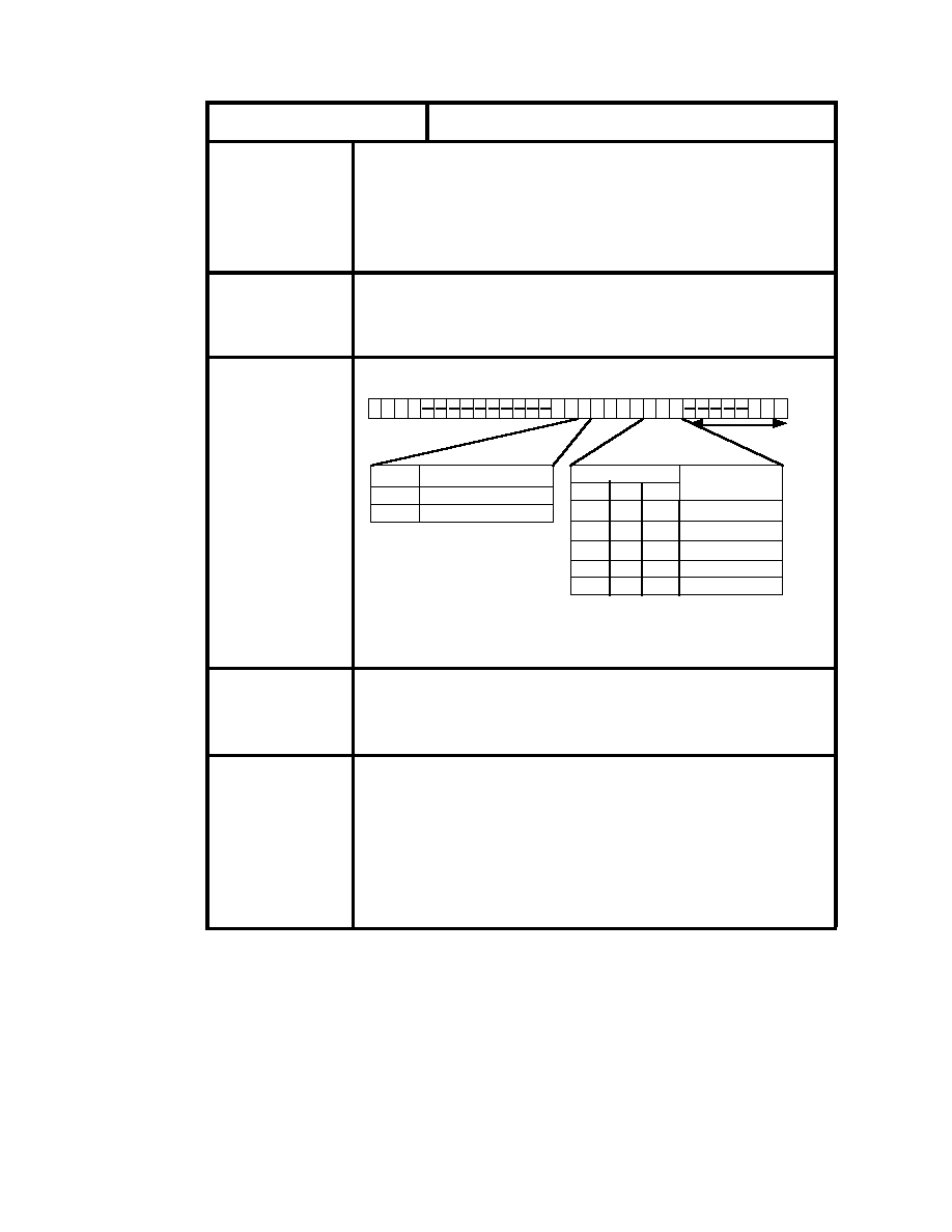
SEGA Confidential
DMAH D0,[RAM],SImm
DMA Transfer (D0[31-0]
RAM) by HOLD Status
Operation
Description
D0[31-0] data is transfered to the RAM. External address register and
transfer word number register save the value at the time transfer
begins. The transfer word number register stores the transfer word
number in long word units. This word number becomes 0 or becomes
the transfer end when forced to end.
Label
DMAH D0,[Destination],[Counter]
Destination = M0~M3 *,PR*
Instruction Code
Flag
T0 ; becomes 1.**
Comments
* [MCx(x=0 ~ 3)] selects DATA RAM x(x=0~3).
PR selects PROGRAM RAM
**When the END signal informing you that transfer end from outside
has been entered, T0; becomes 0.
Designating address-add adds an add number after the command an
becomes DMAH0~DMAH1.
Add number is 1 when address add number designation is omitted.
The transfer source address is set in advance to RA0 and the transfer
destination RAM address is set in advance to CTx.
0
0
b31
x
x
1 1
0
0 1
0
0
7
x
Bit Data
bit9 bit8
RAM Selections
0
0
1
1
0
1
0
1
DATA RAM 0
DATA RAM 1
DATA RAM 2
DATA RAM 3
x
x
x
x
0 0
28
0
0
0
0
bit 10
0
0
PROGRAM RAM
1
Add Mode Selections
Address Add 0
Address Add 1
bit 15
0
1
17 15
SImm Data
Valid only for A-Bus
Address add is 32 bit unit.
137
SCU User's Manual
|

SEGA Confidential
DMAH [RAM],D0,SImm
DMA Transfer (RAM
D0[31-0]) by HOLD Status
Operation
Description
RAM data is transfered to D0[31-0]. The external address register and
transfer word number register save the value when transfer starts.
The transfer word number register is a register for storing the transfer
word number in long word units. This word number is either 0 or
transfer ends when forced to end.
Label
DMA H [Source],D0,Counter
Source = Mo ~ M3 *
Instruction Code
Flag
T0 ; becomes 1.**
Comments
* [MCx(x=0 ~ 3)] selects DATA RAM x(x=0~3).
**When the END signal informing you that transfer end fromoutside
has been entered, T0; becomes 0.
Designating address-add adds an add number after the command and
becomes DMAH0~DMAH64.
Add number is 1 when address add number designation is omitted.
The transfer source RAM address is set in advance to CTx and the
transfer destination address is set in advance to WA0.
0
0
b31
x
x
x
x
Bit Data
bit17 bit16 bit15
Address Add 0
Add Mode Selections
0
0
0
0
1
1
1
1
0
0
1
1
0
0
1
1
0
1
0
1
0
1
0
1
SImm Data
1
17
1
1
0
0 1
0
0
15
7
x
Address Add 1
Address Add 2
Address Add 4
Address Add 8
Address Add 16
Address Add 32
Address Add 64
Bit Data
bit9 bit8
Selections
0
0
1
1
0
1
0
1
DATA RAM 0
DATA RAM 1
DATA RAM 2
DATA RAM 3
138
|

SEGA Confidential
DMAH D0,[RAM],[s]
DMA Transfer (D0[31-0]
RAM
) by HOLD Status
Operation
Description
[s] data designated by bit0~2 is treated as transfer counter, and only
numbers displayed transfer RAM data to D0(31-0) data. External
address register and transfer word number register save the value,
when starting transfer, to the address add number. The transfer word
number register stores transfer word numbers in long word units. This
word number becomes 0 or transfer ends when forced to end.
Label
DMA H D0,[Destination],[Counter]
Counter = M0 ~ M3 *,MC0~MC3*
Destination = M0~M3 *,PR*
Instruction
Code
Valid only for A-Bus
Address add is 32bit units.
Flag
T0 ; becomes 1. **
CTx(x0~3) ; incremented when b2=1. When b2=0, there is no change
Comments
* [MCx(x=0 ~ 3)] selects DATA RAM x(x=0~3). MCx(x=0~3) selects
DATA RAM x(x=0~3), and after transfer increments CTx(x0~3).
**When the END signal informing you that transfer end from outside
has been entered, T0; becomes 0.
Designating address-add adds an add number after the command an
becomes DMAH0~DMAH1.
Add number is 1 when address add number designation is omitted.
The transfer source address is set in advance to RA0 and the transfer
destination RAM address is set in advance to CTx.
0
0
b31
x
x
Bit Data
bit 2 bit1 bit 0
[s] Selections
0
0
0
0
1
1
1
1
0
0
1
1
0
0
1
1
0
1
0
1
0
1
0
1
1 1
0
1 1
0
0
7
x
Bit Data
bit9 bit8
RAM Selections
0
0
1
1
0
1
0
1
DATA RAM 0
DATA RAM 1
DATA RAM 2
DATA RAM 3
DATA RAM 0
DATA RAM 1
DATA RAM 2
DATA RAM 3
DATA RAM 0
DATA RAM 1
DATA RAM 2
DATA RAM 3
,CT0++
,CT1++
,CT2++
,CT3++
x
x
x
x
0 0
28
0
0
0
0
bit 10
0
0
PROGRAM RAM
1
Add Mode Selections
Address Add 0
Address Add 1
bit 15
0
1
139
SCU User's Manual
|
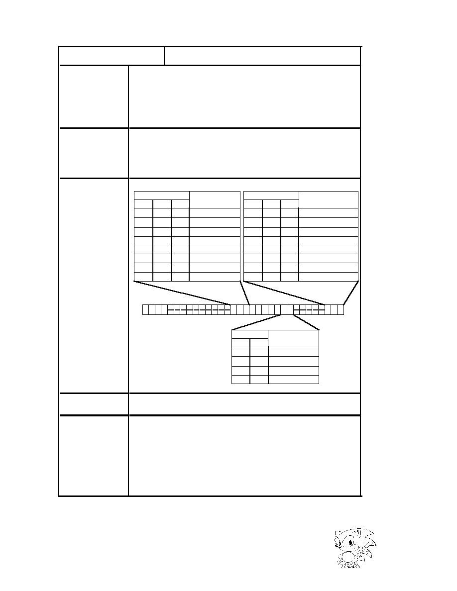
SEGA Confidential
DMA [RAM],D0,[s]
DMA Transfer (RAM
D0[31-0]
) by HOLD Status
Operation
Description
[s] data designated by bit0~2 is treated as transfer counter, and only
numbers displayed transfer RAM data to D0[31-0] data. External
address register and transfer word number register save the value
when starting transfer. The transfer word number register stores
transfer words in long word units. This word number becomes 0 or
transfer ends when forced to end.
Label
DMAH [Source],DO,[Counter]
Counter = M0 ~ M3 *,MC0~MC3*
Source = M0~M3 *,PR*
Instruction
Code
Flag
T0 ; becomes 1. **
CTx(x=0~3) ; incremented when b2=1. No changes when b2=0.
Comments
* [MCx(x=0 ~ 3)] selects DATA RAM x(x=0~3). MCx(x=0~3) selects
DATA RAM x(x=0~3), and after transfer increments CTx(x0~3).
**When the END signal informing you that transfer end from outside
has been entered, T0; becomes 0.
Designating address-add adds an add number after the command and
becomes DMAH0~DMAH64.
Add number is 1 when address add number designation is omitted.
The transfer source RAM address is set in advance to CTx and the
transfer destination address is set in advance to WA0.
0
0
b31
x
x
x
x
Bit Data
bit17 bit16 bit15
Address Add 0
Add Mode
Selections
0
0
0
0
1
1
1
1
0
0
1
1
0
0
1
1
0
1
0
1
0
1
0
1
1
17
1
1
0
1
0
0
7
x
Address Add 1
Address Add 2
Address Add 4
Address Add 8
Address Add 16
Address Add 32
Address Add 64
Bit Data
bit9 bit8
RAM Selections
0
0
1
1
0
1
0
1
DATA RAM 0
DATA RAM 1
DATA RAM 2
DATA RAM 3
1
x
x
x
Bit Data
bit 2 bit1 bit 0
[s] Selections
0
0
0
0
1
1
1
1
0
0
1
1
0
0
1
1
0
1
0
1
0
1
0
1
Data RAM 0
Data RAM 1
Data RAM 2
Data RAM 3
Data RAM 0
Data RAM 1
Data RAM 2
Data RAM 3
,CT0++
,CT1++
,CT2++
,CT3++
140
|

SEGA Confidential
JUMP Commands
Jump commands are realized by storing immediate data in the program counter.
Figure 4.10 shows the Jump command format. Details of the command are shown in
the next few pages.
1
0 1
31 30 29
26 25 24
0
Status
19 18
1
28 27
8 7
Immediate
Figure 4.10 Jump Command Format
141
SCU User's Manual
|

SEGA Confidential
JMP Imm
Unconditional Jump
Operation
Description
Jumps according to address data (Imm).
Label
JMP [address]
Instruction Code
Flag
No change
Comments
0
0 0 0
0
19
b31
25
1 1
1
0 0 0 0
7
Imm Data
142
|

SEGA Confidential
JMP Z, Imm
Conditional Jump (Z = 1)
Operation
Description
When the Z flag is 1, jump is in accordance with address data (Imm).
Label
JMP Z,[address]
Instruction Code
Flag
No change
Comments
0
0
0
19
b31
25
1 1
1
0 0 0
7
Imm Data
1 1
1
143
SCU User's Manual
|

SEGA Confidential
JMP NZ,Imm
Conditional Jump (Z=0)
Operation
Description
When the Z flag is 0, jump is in accordance with address data (Imm).
Label
JMP NZ,[address]
Instruction Code
Flag
No change
Comments
0
0
0
19
b31
25
1 1
1
0 0 0
7
Imm Data
1
1
0
144
|

SEGA Confidential
JMP S,Imm
Conditional Jump (S=1)
Operation
Description
When the S flag is 1, jump is in accordance with address data (Imm).
Label
JMP S,[address]
Instruction Code
Flag
No change
Comments
0
0
0
19
b31
25
1 1
1
0 0
0
7
Imm Data
1
1
1
145
SCU User's Manual
|
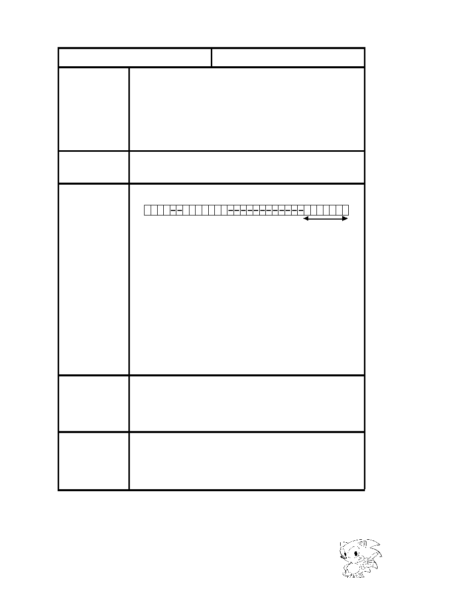
SEGA Confidential
JMP NS,Imm
Conditional Jump (Z=0)
Operation
Description
When the S flag is 0, jump is in accordance with address data (Imm).
Label
JMP NS,[address]
Instruction Code
Flag
No change
Comments
0
0
0
19
b31
25
1 1
1
0 0
0
7
Imm Data
1
1 0
146
|

SEGA Confidential
JMP C,Imm
Conditional Jump (C=1)
Operation
Description
When the C flag is 1, jump is in accordance with address data (Imm).
Label
JMP C,[address]
Instruction Code
Flag
No change
Comments
0
0
0
19
b31
25
1 1
1
0
0
7
Imm Data
1 1
0 1
147
SCU User's Manual
|

SEGA Confidential
JMP NC,Imm
Conditional Jump (C=0)
Operation
Description
When the C flag is 0, jump is in accordance with address data (Imm).
Label
JMP NC,[address]
Instruction Code
Flag
No change
Comments
0
0
0
19
b31
25
1 1
1
0
0
7
Imm Data
1
0 1
0
148
|

SEGA Confidential
JMP T0,Imm
Conditional Jump (T0=1)
Operation
Description
When the T0 flag is 1, jump is in accordance with address data (Imm).
Label
JMP T0,[address]
Instruction Code
Flag
No change
Comments
0
0
0
19
b31
25
1 1
1
0
0
7
Imm Data
1
0
1
1
149
SCU User's Manual
|

SEGA Confidential
JMP NT0,Imm
Conditional Jump (T0=0)
Operation
Description
When the T0 flag is 0, jump is in accordance with address data (Imm).
Label
JMP NT0,[address]
Instruction Code
Flag
No change
Comments
0
0
19
b31
25
1 1
1
0
0
7
Imm Data
1 0
1
0 0
150
|

SEGA Confidential
JMP ZS,Imm
Conditional Jump (Z=1 or S=1)
Operation
Description
When the Z flag or S flag is 1, jump is in accordance with address data
(Imm).
Label
JMP ZS,[address]
Instruction Code
Flag
No change
Comments
0
0
19
b31
25
1 1
1
0
0
7
Imm Data
1
0
1
1
1
151
SCU User's Manual
|

SEGA Confidential
JMP NZS,Imm
Conditional Jump (Z=S=0)
Operation
Description
When the Z flag and S flag are 0, jump is in accordnce with address d
(Imm).
Label
JMP NZS,[address]
Instruction Code
Flag
No change
Comments
0
0
19
b31
25
1 1
1
0
0
7
Imm Data
1
0
1
1
0
152
|

SEGA Confidential
LOOP BOTTOM Commands
Loop Bottom commands repeat one to several steps of a program. Figure 4.11 shows
the Jump command format. Details of the command are shown in the next few
pages.
1
0
1
31 30 29
0
1
28 27
MOD
Figure 4.11 Loop Bottom Command Format
153
SCU User's Manual
|

SEGA Confidential
BTM
Repeat Process Criterion
Operation
Description
There is no repeat when the [LOP] flag is 0. Otherwise the program
counter returns to [TOP].
Does nothing when the [LOP] flag is 0; otherwise, it returns the
program counter to [TOP].
Label
BTM
Instruction Code
Flag
LOP ; decremented when LOP
0. Ends when LOP=0.
Comments
0
0
b31
1 1 1
0
29
27
154
|
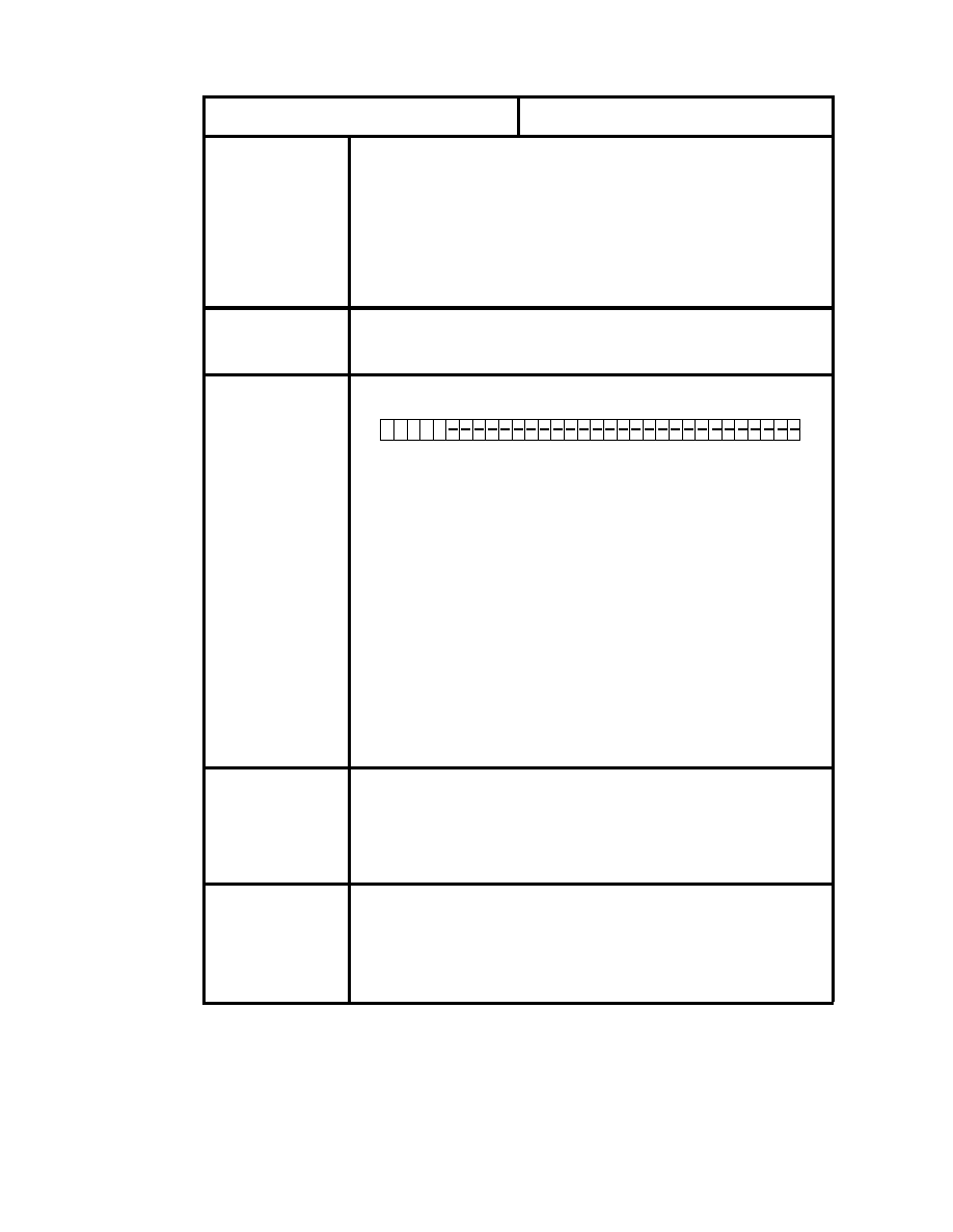
SEGA Confidential
LPS
1 Step Repeat
Operation
Description
Repeats next 1 step until the [LOP] register is 0.
Label
LPS
Instruction Code
Flag
LOP ; decremented when LOP
0. Ends when LOP=0.
Comments
After the process ends, PC executes LOP+1 time then ends.
0
0
b31
1 1 1
29
27
1
155
SCU User's Manual
|

SEGA Confidential
END Command
The END command stops the program currently being executed. Figure 4.12 shows
the END command format. Details of the command are shown in the next two
pages.
1
1
31 30 29
0
1
28 27
1 IE
Figure 4.12 END Command Format
156
|

SEGA Confidential
END
STOP
Operation
Description
Stops the program.
Label
END
Instruction Code
Flag
EX ; is
0.
Comments
0
b31
1 1 1
29
27
1 0
157
SCU User's Manual
|

SEGA Confidential
ENDI
Program End
Operation
Description
Stops the program, and sets the E flag (program end interrupt flag).
Label
ENDI
Instruction Code
Flag
E ; is 1
EX ; is
0.
Comments
0
b31
1 1 1
29
27
1 1
158
|

SEGA Confidential
APPENDIX
This appendix contains a list of SCU register address maps.
159
SCU User's Manual
|

SEGA Confidential
160
Register names are shown in parenthesis.
D1BK
D2WT
D2MV
D1WT
D1MV
DACS0
DACSB
DACSA
D0MV
DOMV
DSTOP
D2FT2
D2FT1
D2FT0
D2GO
D2WUP
D2RUP
D2EN
D2MOD
D2WA1
D2RA
D0GO
D0FT2
D0FT1
D0FT0
D1WA2
D1WA0
D2C10
D2C7
D2C6
D2C4
D2C9
D2C2
D1WUP
D1RUP
D1EN
D2W2
D2W3
D2W7
D2W9
D2W11
D2W12
D2W14
D2W16
D2W18
D2W19
D2W20
D2W22
D2W23
D2W24
D2R13
D2R14
D2R15
D2R16
D2R17
D2R18
D2R19
D2R20
D2R22
D2R23
D2R24
D2R0
D2R1
D2R2
D2R3
D2R4
D2R5
D2R6
D2R7
D2R8
D2R9
D2R10
D2R11
D2R12
D0WUP
D0EN
D0RA
D0WA2
D0WA1
D0WA0
D1C11
D1C10
D1C8
D1C6
D1C5
D1C3
D1C2
D1C0
D1W2
D2W5
D1W6
D1W7
D1W9
D1W10
D1W21
D1W22
D1W25
D1W26
D0C18
D0C17
D0C14
D0C10
D0C9
D0C7
D0C6
D0C5
D0C4
D0C3
D0C0
D0W10
D0W9
D0W8
D0W7
D0W6
D0W4
D0W3
D0W0
D0W15
D0W11
D0R19
D0R18
D0R17
D0R25
D0R23
D0R22
D0R10
D0R9
D0R8
D0R16
D0R15
D0R14
D0R13
D0R7
D0R6
D0R5
D0R4
D0R3
D0R2
D0R1
D0R0
D1R0
D1R1
D1R2
D1R3
D1R4
D1R5
D1R6
D1R7
D1R8
D1R9
D1R13
D1R14
D1R15
D1R16
D1R17
D1R18
D1R19
D1R11
D1R12
D1R21
D1R22
D1R23
D1R24
D1R25
D1R26
D0MOD
D1MOD
D0R26
D0R24
D0R21
D0R20
D0R11
D0R12
D0W26
D0W25
D0W24
D0W22
D0W23
D0W21
D0W20
D0W18
D0W19
D0W17
D0W16
D0W14
D0W13
D0W12
D0W5
D0W2
D0W1
D0C1
D0C2
D0C8
D0C12
D0C13
D0C11
D0C19
D0C16
D0C15
D0RUP
D1R10
D1R20
D1W0
D1W3
D1W4
D1W8
D1W1
D1W11
D1GO
D1WA1
D1RA
D1C1
D1C4
D1C7
D1C9
D1W16
D1W20
D1W19
D1W18
D1W17
D1W15
D1W14
D1W13
D1W12
D1FT2
D1FT1
D1FT0
D0WT
DOWT
D0BK
D2W15
D2W13
D2C11
D2C8
D2C5
D2C3
D2C1`
D2C0
D2WA0
D2WA2
D2W6
D2W5
D2W4
D2W1
D2W0
D2W8
D2W10
D2W17
D2W21
D2R21
D2W25
D2R26
D2R25
D1W24
D1W23
D2W26
|

SEGA Confidential
161
SCU User's Manual
EP
PR
PD31
PD30
PD29
PD28
PD27
PD26
PD25
PD24
PD23
PD22
PD21
PD20
PD19
PD18
PD17
PD16
PD15
PD14
PD13
T0
Z
V
E8
LE
9
C
E
EX
RD31
RD30
RD29
RD28
RD27
RD26
RD25
RD24
RD23
RD22
RD21
RD20
RD19
RD18
RD17
RD16
RD15
RD14
RD13
PD12
PD11
PD10
PD9
PD8
PD7
PD6
PD5
PD4
PD3
PD2
PD1
PD0
RD12
RD11
RD10
RD9
RD8
RD7
RD6
RD5
RD4
RD3
RD2
RD1
RD0
P7
P6
P5
P4
P3
P2
P1
P0
RA7
RA6
RA5
RA4
RA3
RA2
RA1
RA0
T0C9
T0C8
T0C7
T0C6
T0C5
T0C4
T0C3
T0C2
T0C1
T0C0
T198
T197
T196
T195
T194
T193
T192
T191
T190
T1MD
TENB
VER3
VER2
VER1
VER0
RSEL
ARWT3
ARWT2
ARWT1
ARWT0
ARFEN
IST28
IST27
IST26
IST10
IST9
IST8
IST7
IST6
IST5
IST4
IST3
IST2
IST1
IST0
AIACK
IMS13
IMS12
IMS11
IMS10
IMS9
IMS8
IMS7
IMS6
IMS5
IMS4
IMS3
IMS2
IMS1
IMS0
A0SZ
A1PRO
A1WPC
A1RPC
A1EW1
A1BW3
A1BW2
A1BW1
A1BW0
A1NW3
A1NW2
A1NW1
A1NW0
A1LN1
A1LN0
A1SZ
A2SZ
A3PRO
A3WPC
A3RPC
A3EW1
A3BW3
A3BW2
A3BW1
A3BW0
A3NW3
A3NW2
A3NW1
A3NW0
A3LN1
A3LN0
A3SZ
A2LN1
A2LN0
A2PRO
A2WPC
A2RPC
A2EWT
IMS15
IST31
IST30
IST29
IST25
IST24
IST23
IST13
IST12
IST11
IST22
IST21
IST20
IST19
IST18
IST17
IST16
A0PRO
A0WPC
A0RPC
A0EWT
A0BW3
A0BW2
A0BW1
A0BW0
A0NW3
A0NW2
A0NW1
A0NW0
A0LN1
A0LN0
25FE0080(PPAF)
25FE0084(PPD)
25FE0088(PDA)
25FE008C(PDD)
25FE0090(T0C)
25FE0094(T1S)
25FE009C(--)
25FE0098(T1MD)
25FE00A0(IMS)
25FE00A4(IST)
25FE00A8(--)
25FE00AC(--)
25FE00B0(ASR0)
25FE00B4(ASR1)
25FE00B8(AREF)
25FE00BC(AIAK)
25FE00C0(--)
25FE00C4(RSEL)
25FE00C8(VER)
25FE00CC(--)
|

SEGA Confidential
Acronym
Address
Bit
Description
AIACK
25FE00A8
H
0
A-Bus interrupt acknowledge output valid bit
(=0: invalid / =1: valid)
ARFEN
25FE00B8
H
4
A-Bus refresh output valid bit (=0: invalid/=1: valid)
ARWT3-0
25FE00B8
H
3 - 0
A-Bus refresh wait number
A0BW3-0
25FE00B0
H
27 - 24
CS0 space, burst cycle wait number set bit
A0EWT
25FE00B0
H
28
CS0 space, external wait effective bit (=0: invalid/=1: valid)
A0LN1-0
25FE00B0
H
19 - 18
CS0 space, burst length set bit
A0PRD
25FE00B0
H
31
CS0 space, previous read effective bit (=0: invalid/=1: valid)
A0RPC
25FE00B0
H
29
CS0 space, pre-charge insert bit after read
A0NW3-0
25FE00B0
H
23 - 20
CS0 space, normal cycle wait number set bit
A0SZ
25FE00B0
H
16
CS0 space, bus size set bit
A0WPC
25FE00B0
H
30
CS0 space, pre-charge insert bit after write
A1BW3-0
25FE00B0
H
11 - 8
CS1 space, burst cycle wait number set bit
A1EWT
25FE00B0
H
12
CS1 space, external wait effctive bit (=0: invalid/=1: valid)
A1LN1-0
25FE00B0
H
3 - 2
CS1 space, burst length set bit
A1NW3-0
25FE00B0
H
7 - 4
CS1 space, normal cycle wait number set bit
A1PRD
25FE00B0
H
15
CS1 space, previous read effective bit (=0: invalid/=1: valid)
A1RPC
25FE00B0
H
13
CS1 space, pre-charge insert bit after read
A1SZ
25FE00B0
H
0
CS1 space, bus size set bit
A1WPC
25FE00B0
H
14
CS1 space, pre-charge insert bit after write
A2EWT
25FE00B4
H
28
CS2 space, external wait effctive bit (=0: invalid/=1: valid)
A2LN1-0
25FE00B4
H
19 - 18
CS2 space, burst length set bit
A2PRD
25FE00B4
H
31
CS2 space, previous read effective bit (=0: invalid/=1: valid)
A2RPC
25FE00B4
H
29
CS2 space, pre-charge insert bit after read
A2SZ
25FE00B4
H
16
CS2 space, bus size set bit
A2WPC
25FE00B4
H
30
CS2 space, pre-charge insert bit after write
A3BW3-0
25FE00B4
H
11 - 8
Dummy space, burst cycle wait number set bit
A3EWT
25FE00B4
H
12
Dummy space, external wait effctive bit
(=0: invalid/=1: valid)
A3LN1-0
25FE00B4
H
3 - 2
Dummy space, burst length set bit
A3NW3-0
25FE00B4
H
7 - 4
Dummy space, normal cycle wait number set bit
A3PRD
25FE00B4
H
15
Dummy space, previous read effective bit (=0: invalid/=1: valid)
A3RPC
25FE00B4
H
13
Dummy space, pre-charge insert bit after read
A3SZ
25FE00B4
H
0
Dummy space, bus size set bit
A3WPC
25FE00B4
H
14
Dummy space, pre-charge insert bit after write
C
25FE0080
H
20
DSP program control port, Carry flag
DACSA
25FE007C
H
20
DMA A-Bus Access Flag (=0: no access/=1: access)
DACSB
25FE007C
H
21
DMA B-Bus Access Flag (=0: no access/=1: access)
DACSD
25FE007C
H
22
DMA DSP-Bus Access Flag (=0: no access/=1: access)
DDMV
25FE007C
H
0
DSP side DMA operate flag (=0: stop/=1: operate)
DDWT
25FE007C
H
1
DSP side DMA standby flag (=0: stop/=1: standby)
DSTOP
25FE0060
H
0
DMA force-stop bit (=0: DMA operable/=1: DMA force stop)
D0BK
25FE007C
H
16
DMA level 0 interrupt flag (=0: stop/=1: interrupt)
D0C19-0
25FE0008
H
19 - 0
DMA level 0 transfer byte number
D0EN
25FE0010
H
8
DMA level 0 enable bit (=0: Disable/=1: Enable)
162
|

SEGA Confidential
Acronym
Address
Bit
Description
D0FT2-0
25FE0014
H
2 - 0
DMA level 0 starting factor selection bit
=000B: V-Blank-IN receive and enable bit set
=001B: V-Blank-OUT receive and enable bit set
=010B: H-Blank-IN receive and enable bit set
=011B: Timer 0 receive and enable bit set
=100B: Timer 1 receive and enable bit set
=101B: Sound Req receive and enable bit set
=110B: Sprite draw end and enable bit set
=111B: DMA start bit set and enable bit set
D0GO
25FE0010
H
0
DMA level 0 start bit (=0: stop =1: start)
D0MOD
25FE0014
H
24
DMA level 0 mode bit (=0: direct mode/=1: indirect mode)
D0MV
25FE007C
H
4
DMA level 0 operating flag (=0: stop/=1: start)
D0RA
25FE000C
H
8
DMA level 0 read address add value
(=0: no add/=1: adds 4 byte)
D0RUP
25FE0014
H
16
DMA level 0 read address update bit
D0R26-0
25FE0000
H
26 - 0
DMA level 0 read address
D0WA2-0
25FE000C
H
2 - 0
DMA level 0 write address add value
=000
B
: no addition
=001
B
: adds 2 bytes
=010
B
: adds 4 bytes
=011
B
: adds 8 bytes
=100
B
: adds 16 bytes
=101
B
: adds 32 bytes
=110
B
: adds 64 bytes
=111
B
: adds 128 bytes
D0WT
25FE007C
H
5
DMA level 0 standby flag (=0: stop/=1: standby)
D0WUP
25FE0014
H
8
DMA level 0 write address update bit
D0W26-0
25FE0004
H
26 - 0
DMA level 0 write address
D1BK
25FE007C
H
17
DMA level 1 interrupt flag (=0: stop/=1: interrupt)
D1C11-0
25FE0028
H
11 - 0
DMA level 1 transfer byte number
D1EN
25FE0030
H
8
DMA level 1 enable bit (=0: Disable/=1: Enable)
D1FT2-0
25FE0034
H
2 - 0
DMA level 1 starting factor selection bit
=000B: V-Blank-IN receive and enable bit set
=001B: V-Blank-OUT receive and enable bit set
=010B: H-Blank-IN receive and enable bit set
=011B: Timer 0 receive and enable bit set
=100B: Timer 1 receive and enable bit set
=101B: Sound Req receive and enable bit set
=110B: Sprite draw end and enable bit set
=111B: DMA start bit set and enable bit set
D1GO
25FE0030
H
0
DMA level 1 start bit (=0: stop/=1: start)
D1MOD
25FE0034
H
24
DMA level 1 mode bit (=0: direct mode/=1: indirect mode)
D1MV
25FE007C
H
8
DMA level 1 operating flag (=0: stop/=1: start)
D1RA
25FE002C
H
8
DMA level 1 read address add value
(=0: no add/=1: adds 4 bytes)
D1RUP
25FE0034
H
16
DMA level 1 read address update bit
D1R26-0
25FE0020
H
26 - 0
DMA level 1 read address
163
SCU User's Manual
|

SEGA Confidential
Acronym
Address
Bit
Description
D1WA2-0
25FE002C
H
2 - 0
DMA level 1 write address add value
=000
B
:does not add
=001
B
: adds 2 bytes
=010
B
: adds 4 bytes
=011
B
: adds 8 bytes
=100
B
: adds 16 bytes
=101
B
: adds 32 bytes
=110
B
: adds 64 bytes
=111
B
: adds 128 bytes
D1WT
25FE007C
H
9
DMA level 1 standby flag (=0: stop/=1: standby)
D1WUP
25FE0034
H
8
DMA level 1 write address update bit
D1W26-0
25FE0024
H
26 - 0
DMA level 1 write address
D2C11-0
25FE0048
H
11 - 0
DMA level 2 transfer byte number
D2EN
25FE0050
H
8
DMA level 2 enable bit (=0: Disable/=1: Enable)
D2FT2-0
25FE0054
H
2 - 0
DMA level 2 starting factor selection bits
=000
B
: V-Blank-IN receive and enable bit set
=001
B
: V-Blank-OUT receive and enable bit set
=010
B
: H-Blank-IN receive and enable bit set
=011
B
: Timer 0 recieve and enable bit set
=100
B
: Timer 1 recieve and enable bit set
=101
B
: Sound Req receive and enable bit set
=110
B
: Sprite draw end and enable bit set
=111
B
: DMA start bit set and enable bit set
D2G0
25FE0050
H
0
DMA level 2 start bit (=0: stop/=1: operation)
D2MOD
25FE0054
H
24
DMA level 2 mode bit (=0: direct mode/=1: indirect mode)
D2MV
25FE007C
H
12
DMA level 2 operation flag (=0: stop/=1: operation)
D2RA
25FE004C
H
8
DMA level 2 read address add value
(=0: no add/=1: adds 4 bytes)
D2RUP
25FE0054
H
16
DMA level 2 read address update bit
D2R26-0
25FE0040
H
26 - 0
DMA level 2 read address
D2WA2-0
25FE004C
H
2 - 0
DMA level 2 write address add value
=000
B
: no addition
=001
B
: adds 2 bytes
=010
B
: adds 4 bytes
=011
B
: adds 8 bytes
=100
B
: adds 16 bytes
=101
B
: adds 32 bytes
=110
B
: adds 64 bytes
=111
B
: adds 128 bytes
D2WT
25FE007C
H
13
DMA level 2 standby flag (=0: stop/=1: standby)
D2WUP
25FE0054
H
8
DMA level 2 write address update bit
D2W26-0
25FE0044
H
26 - 0
DMA level 2 write address
E
25FE0080
H
18
DSP Program control port, Program end interrupt flag
EP
25FE0080
H
25
DSP Program control port, Temporary stop execution flag during
program execution
(=0: don't execute / =1: execute)
164
|

SEGA Confidential
Acronym
Address
Bit
Description
ES
25FE0080
H
17
DSP Program Control Port, Program Step Execution Control Bit
(=0: don't execute / =1: execute)
EX
25FE0080
H
16
DSP Program Control Port, Program Execution Control Bit
(=0: don't execute / =1: execute)
IMS0
25FE00A0
H
0
V-Blank-IN Interrupt Mask Bit
IMS1
25FE00A0
H
1
V-Blank-OUT Interrupt Mask Bit
IMS2
25FE00A0
H
2
H-Blank-IN Interrupt Mask Bit
IMS3
25FE00A0
H
3
Timer 0 Interrupt Mask Bit
IMS4
25FE00A0
H
4
Timer 1 Interrupt Mask Bit
IMS5
25FE00A0
H
5
DSP End Interrupt Mask Bit
IMS6
25FE00A0
H
6
Sound Request Interrupt Mask Bit
IMS7
25FE00A0
H
7
SMPC Interrupt Mask Bit
IMS8
25FE00A0
H
8
PAD Interrupt Mask Bit
IMS9
25FE00A0
H
9
Level 2-DMA End Interrupt Mask Bit
IMS10
25FE00A0
H
10
Level 1-DMA End Interrupt Mask Bit
IMS11
25FE00A0
H
11
Level 0-DMA End Interrupt Mask Bit
IMS12
25FE00A0
H
12
DMA Illegal Interrupt Mask Bit
IMS13
25FE00A0
H
13
Sprite Draw End Interrupt Mask Bit
IMS15
25FE00A0
H
15
A-Bus Interrupt Mask Bit
IST0
25FE00A4
H
0
V-Blank-IN Interrupt Status Bit
IST1
25FE00A4
H
1
V-Blank-OUT Interrupt Status Bit
IST2
25FE00A4
H
2
H-Blank-IN Interrupt Status Bit
IST3
25FE00A4
H
3
Timer 0 Interrupt Status Bi
t
IST4
25FE00A4
H
4
Timer 1 Interrupt Status Bit
IST5
25FE00A4
H
5
DSP End Interrupt Status Bit
IST6
25FE00A4
H
6
Sound request Interrupt Status Bit
IST7
25FE00A4
H
7
SMPC Interrupt Status Bit
IST8
25FE00A4
H
8
PAD Interrupt Status Bit
IST9
25FE00A4
H
9
Level 2-DMA End Interrupt Status Bit
IST10
25FE00A4
H
10
Level 1-DMA End Interrupt Status Bit
IST11
25FE00A4
H
11
Level 0-DMA End Interrupt Status Bit
IST12
25FE00A4
H
12
DMA Illegal Interrupt Status Bit
IST13
25FE00A4
H
13
Sprite Draw End Interrupt Status Bit
IST31-16
25FE00A4
H
31-16
Outside Interrupt 15-0 Status Bit
LE
25FE0080
H
15
DSP Program Control Port, Program Counter Load Enable Bit (=0:
no execute/=1: execute)
PD31-0
25FE0084
H
31 - 0
DSP Program RAM Data Port
PR
25FE0080
H
26
DSP Program Control Port, Pause Cancel Flag while program is
executing (=0: no execute/=1: execute)
P7-0
25FE0080
H
7 - 0
DSP Program RAM Address
RA7-0
25FE0088
H
7 - 0
DSP Data RAM Address
RD31-0
25FE008C
H
31 - 0
DSP Data RAM Data Port
RSEL
25FE00C4
H
0
SDRAM Selection Bit (=0: 2 Mbit x 2 / =1: 4 Mbit x 2)
S
25FE0080
H
22
DSP Program Control Port, Sine Flag
165
SCU User's Manual
|

SEGA Confidential
TENB
25FE0098
H
0
Timer Enable Bit (=0: OFF / =1: ON)
T0
25FE0080
H
23
DSP Program Control Port, D0 Bus Use DMA Execute Flag
T0C9-0
25FE0090
H
9 - 0
Timer 0 Compare Data
T1MD
25FE0098
H
8
Timer 1 ModeBit
=0: occurs at each line
=1: occurs only at lines indicated by Timer 0
T1S8-0
25FE0094
H
8 - 0
Timer 1 Set Data
V
25FE0080
H
19
DSP Program Control Port, Overflow Flag
VER3-0
25FE00C8
H
3 - 0
SCU Chip Version Number
Z
25FE0080
H
21
DSP Program Control Port, Zero Flag
166
|

SEGA Confidential
INDEX
Numbers within ( ) shows the page of the "First" heading.
Numeric
1 command Repeat Execution...................................................................................... 89
Alphabetic
A-Bus ................................................................................................................................ ii
A-Bus Control Register ................................................................................................. 61
A-Bus Interrupt Acknowledge .................................................................................... 61
A-Bus Interrupt Acknowledge Register ..................................................................... 61
A-Bus Interrupt Acknowledge Map ........................................................................... 14
A-Bus Refresh Register ........................................................................................... 13, 71
A-Bus Refresh Register Map ........................................................................................ 13
A-Bus Refresh Wait Number ........................................................................................ 71
A-Bus Set Register (CS0, 1 spaces) .............................................................................. 62
A-Bus Set Register (CS2 and dummy spaces) ........................................................... 62
A-Bus Set Register Map ................................................................................................ 13
Access, Interrupt, Standby, Operation Registers ....................................................... 47
B-Bus ............................................................................................................................... (ii)
Blanking Interrupt ......................................................................................................... 29
Block Diagram .................................................................................................................. 3
Commands ...................................................................................................................... 91
Commands (1), List of ................................................................................................... 80
Commands (2), List of ................................................................................................... 81
Commands (3), List of ................................................................................................... 82
Commands (4), List of ................................................................................................... 83
Constants, Description of ............................................................................................. 90
CS0 Space Burst Cycle Set Value ................................................................................. 65
CS0 Space Burst Length Set Value ............................................................................... 65
CS0 Space Bus Size Set Value ....................................................................................... 66
CS0 Space Single Cycle Set Value ................................................................................ 65
CS0, 1 Space A-Bus Set Set Register ............................................................................ 62
CS1 Space Burst Cycle Set Value ................................................................................. 67
CS1 Space Burst Length Set Value ............................................................................... 68
CS1 Space Bus Size Set Value ....................................................................................... 68
CS1 Space Single Cycle Set Value ................................................................................ 67
CS2 Space Burst Cycle Value ........................................................................................ 68
CS2 Space Bus Size Set Value ....................................................................................... 70
167
SCU User's Manual
|

SEGA Confidential
Data .................................................................................................................................... ii
Data Write Example (Indirect Mode) .......................................................................... 23
Difference in DMA operation by Address Renewal Bit ........................................... 22
Difference in Timing by Setting External Wait Effective Bit .................................... 64
Direct Mode DMA Transfer Operation ...................................................................... 18
DMA Enable Register .................................................................................................... 45
DMA Command Execution .......................................................................................... 87
DMA Command Format 1 ......................................................................................... 132
DMA Command Format 2 ......................................................................................... 132
DMA Control Register .................................................................................................. 41
DMA End Interrupt ....................................................................................................... 33
DMA Force-Stop Register ............................................................................................. 47
DMA Force-Stop Register Map...................................................................................... 8
DMA Illegal Interrupt ................................................................................................... 33
DMA Mode ..................................................................................................................... 18
DMA Mode, Address Renewal, Start Factor Select Register ................................... 46
DMA Status Register ............................................................................................... 47, 48
DMA Status Register Map .............................................................................................. 9
DMA Transfer (Basic Operation) ................................................................................. 16
DMA Transfer Execution by Address Add Value Set ............................................... 26
DMA Transferable Area when Started from DSP ..................................................... 17
DMA Transferable Area when Started from Main CPU .......................................... 17
DMA Write Address while Stopped ........................................................................... 46
DSP .................................................................................................................................. 34
DSP Control Port............................................................................................................ 51
DSP Data RAM Address Port ................................................................................ 10, 53
DSP Data RAM Address Port Map ............................................................................. 10
DSP Data RAM Data Port ............................................................................................. 54
DSP Data RAM Data Port Map ................................................................................... 10
DSP End Interrupt ......................................................................................................... 33
DSP Program Control Port ............................................................................................. 9
DSP Program Load Step 1 ............................................................................................ 34
DSP Program Load Step 2 ............................................................................................ 35
DSP Program Load Step 3 ............................................................................................ 35
DSP Program RAM Data Port ................................................................................ 10, 53
DSP Program RAM Data Port Map ............................................................................ 10
Dummy Space Burst Cycle Set Value ......................................................................... 71
Dummy Space Burst Length Set Value ....................................................................... 71
Dummy Space Bus Size Set Value ............................................................................... 72
Dummy Space Single Cycle Set Value ........................................................................ 71
168
|

SEGA Confidential
Example of transfer between SCU and Processor ..................................................... 44
Features of Data Transfer to DSP from D0 Bus ................................................... 87, 88
High/Low Level DMA Operation .............................................................................. 48
Indirect Mode DMA Transfer ...................................................................................... 20
Indirect Mode DMA Transfer Flow............................................................................. 19
Interrupt Control Register ............................................................................................ 57
Interrupt Factor .............................................................................................................. 27
Interrupt Factor, General Names ................................................................................. 28
Interrupt Mask Register ................................................................................................ 57
Interrupt Mask Register Map ....................................................................................... 12
Interrupt Status Register ............................................................................................... 58
Interrupt Status Register Contents .............................................................................. 59
Interrupt Status Register Map ..................................................................................... 12
Jump Command Execution .......................................................................................... 85
Jump Command Format ............................................................................................. 141
Level 0 Transfer Byte Number ..................................................................................... 42
Level 2-0 Address Add Value ....................................................................................... 42
Level 2-0 DMA Authorization Bit ............................................................................... 45
Level 2-0 DMA Mode, Address Renewal, Start Factor Select Register .................. 46
Level 2-0 DMA Set Register Map .................................................................................. 8
Level 2-0 Read Address ................................................................................................ 41
Level 2-0 Write Address ................................................................................................ 41
Level 2-1 Transfer Byte Number .................................................................................. 42
Load Immediate Command Format 1 (unconditional transfer) ........................... 120
Load Immediate Command Format 2 (conditional transfer) ................................ 120
Loop Bottom Command Format ............................................................................... 153
Loop Program Execution .............................................................................................. 86
Main CPU .......................................................................................................................... i
Operand Execution Method ......................................................................................... 85
Operation Command Format ...................................................................................... 91
Operation when Cache Hit............................................................................................. 5
PAD Interrupt ................................................................................................................. 33
RAM Page Select ............................................................................................................ 53
Read Address Add Value .............................................................................................. 43
Registers, List of ............................................................................................................. 40
Results of Previous Read Process ................................................................................ 63
169
SCU User's Manual
|

SEGA Confidential
SCSP .................................................................................................................................... i
SCU ..................................................................................................................................... i
SCU Control Register .................................................................................................... 73
SCU Mapping (Cache_address)..................................................................................... 4
SCU Mapping (Cache_through_address) .................................................................... 6
SCU Overview ................................................................................................................. 2
SCU SDRAM Select Register Map .............................................................................. 14
SCU SDRAM Select Bit ................................................................................................. 73
SCU Version Register Map ........................................................................................... 14
SCU Version Register .................................................................................................... 73
SMPC ................................................................................................................................. ii
SMPC Interrupt .............................................................................................................. 33
Sound Request Interrupt .............................................................................................. 33
Special Process Execution ............................................................................................. 89
Sprite Draw End Interrupt ........................................................................................... 33
Start Factor ...................................................................................................................... 46
Subroutine Program Execution .................................................................................... 90
System Configuration ..................................................................................................... 2
Timer 0 Compare Register ...................................................................................... 11, 55
Timer 0 Compare Register Map ................................................................................... 11
Timer 0 Interrupt Degree of Occurrence .................................................................... 30
Timer 1 Interrupt Degree of Occurrence .................................................................... 31
Timer 1 Mode Register ............................................................................................ 11, 56
Timer 1 Mode Register Map ......................................................................................... 11
Timer 1 Occurrence Select Content ............................................................................. 56
Timer 1 Set Data Register ....................................................................................... 11, 55
Timer 1 Set Data Register Map .................................................................................... 11
Timer Operation Contents ............................................................................................ 56
Timer Register ................................................................................................................ 55
Timing when setting pre-charge insert bit after Read .............................................. 63
Timing when setting pre-charge insert bit after Write ............................................. 63
Timing when Writing CS2 Burst Cycle ....................................................................... 65
VDP1 ................................................................................................................................... i
VDP2 ................................................................................................................................... i
Work RAM Area Contents ............................................................................................ 24
Write Address Add Value ............................................................................................. 43
Write Address Add Value Indication .......................................................................... 45
170
|

SEGA Confidential
(This page is blank in the original Japanese document.)
171
SCU User's Manual
|

SEGA Confidential
Commands
NOP (ALU Operation) .................................................................................................. 93
AND ................................................................................................................................. 94
OR .................................................................................................................................... 95
XOR .................................................................................................................................. 96
ADD ................................................................................................................................. 97
SUB .................................................................................................................................. 98
AD2 .................................................................................................................................. 99
SR ................................................................................................................................... 100
RR ................................................................................................................................... 101
SL .................................................................................................................................... 102
RL ................................................................................................................................... 103
RL8 ................................................................................................................................. 104
NOP (X-Bus Operation) .............................................................................................. 106
MOV [s] , X ................................................................................................................... 107
MOV MUL , p ............................................................................................................... 108
MOV [s] , P.................................................................................................................... 109
NOP (Y-Bus Control) ...................................................................................................111
MOV [s] , Y ................................................................................................................... 112
CLR A ........................................................................................................................... 113
MOV ALU , A ............................................................................................................... 114
MOV [s] , A ................................................................................................................... 115
NOP (D1-Bus No Operation) .................................................................................... 117
MOV SImm , [d] ........................................................................................................... 118
MOV [s] , [d] ................................................................................................................. 119
MVI Imm , [d] ............................................................................................................... 121
MVI [d] , Imm , Z ......................................................................................................... 122
MVI Imm , [d] , NZ ...................................................................................................... 123
MVI Imm , [d] , S ......................................................................................................... 124
MVI Imm , [d] , NS ...................................................................................................... 125
MVI Imm , [d] , C ......................................................................................................... 126
MVI Imm , [d] , NC ..................................................................................................... 127
MVI Imm , [d] , T0 ....................................................................................................... 128
MVI Imm , [d] , NT0 .................................................................................................... 129
MVI Imm , [d] , ZS ....................................................................................................... 130
MVI Imm , [d] , NZS ................................................................................................... 131
172
|

SEGA Confidential
DMA D0 , [RAM] , SImm .......................................................................................... 133
DMA [RAM] , D0 , SImm .......................................................................................... 134
DMA , D0 , [RAM] , [s] .............................................................................................. 135
DMA [RAM] , D0 , [s] ................................................................................................ 136
DMAH , D0 , [RAM] , SImm ..................................................................................... 137
DMAH [RAM] , D0 , SImm ....................................................................................... 138
DMAH D0 , [RAM] , [s] ............................................................................................. 139
DMAH [RAM] , D0 , [s] ............................................................................................. 140
JMP Imm ...................................................................................................................... 142
JMP Z , Imm................................................................................................................. 143
JMP NZ , Imm ............................................................................................................. 144
JMP S , Imm ................................................................................................................. 145
JMP NS , Imm .............................................................................................................. 146
JMP C , Imm ................................................................................................................ 147
JMP NC , mm .............................................................................................................. 148
JMP T0 , Imm ............................................................................................................... 149
JMP NT0 , Imm ........................................................................................................... 150
JMP ZS , Imm .............................................................................................................. 151
JMP NZS , Imm ........................................................................................................... 152
BTM ............................................................................................................................... 154
LPS ................................................................................................................................. 155
END ............................................................................................................................... 157
ENDI ........................................................................................................................ 33, 158
173
SCU User's Manual
|