SEGA Confidential
General Notice
When using this document, keep the following in mind:
1. This document is confidential. By accepting this document you acknowledge that you are bound
by the terms set forth in the non-disclosure and confidentiality agreement signed separately and /in
the possession of SEGA. If you have not signed such a non-disclosure agreement, please contact
SEGA immediately and return this document to SEGA.
2. This document may include technical inaccuracies or typographical errors. Changes are periodi-
cally made to the information herein; these changes will be incorporated in new versions of the
document. SEGA may make improvements and/or changes in the product(s) and/or the
program(s) described in this document at any time.
3. No one is permitted to reproduce or duplicate, in any form, the whole or part of this document
without SEGA'S written permission. Request for copies of this document and for technical
information about SEGA products must be made to your authorized SEGA Technical Services
representative.
4. No license is granted by implication or otherwise under any patents, copyrights, trademarks, or
other intellectual property rights of SEGA Enterprises, Ltd., SEGA of America, Inc., or any third
party.
5. Software, circuitry, and other examples described herein are meant merely to indicate the character-
istics and performance of SEGA's products. SEGA assumes no responsibility for any intellectual
property claims or other problems that may result from applications based on the examples
describe herein.
6. It is possible that this document may contain reference to, or information about, SEGA products
(development hardware/software) or services that are not provided in countries other than Japan.
Such references/information must not be construed to mean that SEGA intends to provide such
SEGA products or services in countries other than Japan. Any reference of a SEGA licensed prod-
uct/program in this document is not intended to state or simply that you can use only SEGA's
licensed products/programs. Any functionally equivalent hardware/software can be used instead.
7. SEGA will not be held responsible for any damage to the user that may result from accidents or any
other reasons during operation of the user's equipment, or programs according to this document.
(6/27/95- 002)
NOTE: A reader's comment/correction form is provided with this
document. Please address comments to :
SEGA of America, Inc., Developer Technical Support (att. Evelyn Merritt)
150 Shoreline Drive, Redwood City, CA 94065
SEGA may use or distribute whatever information you supply in any way
it believes appropriate without incurring any obligation to you.
|

SEGA Confidential
TM
© 1994 SEGA. All Rights Reserved.
Saturn
SCSP
User's Manual
Doc. # ST-77-R2-052594
|
SEGA Confidential
READER CORRECTION/COMMENT SHEET
Chpt.
pg. #
Correction
Corrections:
General Information:
Your Name
Phone
Document number
Date
Document name
Questions/comments:
Keep us updated!
If you should come across any incorrect or outdated information while reading through the attached
document, or come up with any questions or comments, please let us know so that we can make the
required changes in subsequent revisions. Simply fill out all information below and return this form to
the Developer Technical Support Manager at the address below. Please make more copies of this form if
more space is needed. Thank you.
Fax:
(415) 802-3963
Attn: Manager,
Developer Technical Support
Mail:
SEGA OF AMERICA
Attn: Manager,
Developer Technical Support
275 Shoreline Dr. Ste 500
Redwood City, CA 94065
Where to send your corrections:
ST-77-R2-052594
Saturn SCSP User's Manual
|

SEGA Confidential
History
First Edition: (November 30, 1993)
· New manual
Second Edition:
(January 8, 1994)
· Corrected page numbers
Third Edition:
(February 24, 1994)
· Revisions based on the Feb. 8, 1994, meeting.
|

SEGA Confidential
Introduction
Definitions
Terms used in this manual are defined below.
SCSP (Saturn Custom Sound Processor)
A multi-function game sound generator LSI that combines a PCM
sound generator and sound DSP.
Data
A bit indicates 0 or 1 and is the smallest unit. 8 bits combined
together is called a byte, and 16 bits (or 2 bytes) is called a word.
When upper and lower grade is divided into 4 bits respectively,
they are called nibbles.
PAN-POT
Determines the direction or location from which the sound seems to
come from in localization.
Direct Data
Sound that does not pass through the DSP, or even if it did, no
effects were applied. Also called "dry data".
Effect Data
The sound generated, as a result of sending it through DSP with an
effect created in the sound generator. Also called "wet data".
MIDI Standard (Musical Instrument Digital Interface)
Conversion standard for sound interval and sound length used to
communicate between electronic instruments and computers.
Pulse Code Modulation Sound Generator
Sound is converted to PCM data and stored in memory. Refers to
the sound source in a method by which sound data is read from
memory during performance to generate the sound output. PCM
divides the sound (wave form) along the time axis and converts
each of the wave high values to digital data. The data that results
from this operation is called PCM data.
FM (Frequency Modulation)
Indicates frequency modulation. In the context of a sound genera-
tor, it indicates the FM sound generator.
i
|

SEGA Confidential
Linear
Shows a straight line. This means that the relation of the input and
output are proportional. Therefore, if the wave form data is linear,
a high wave value proportional to the size of the data is produced.
In other words, the quantized step is in equal intervals.
LFO (Low Frequency Oscillator)
Indicates a functional frequency generator that generates wave
forms with frequencies that are below the range that is audible to
the human ear. The output wave form of this LFO is used for
amplitude and modulation of frequency.
DSP (Digital Signal Processor)
This is mainly for calculation (multiplication and addition) and
contains a circuit for high-speed calculations. The DSP within
SCSP is specially customized for audio editing functions and is
used when directing sound effects such as echo, reverb, chorus and
filter.
Sample Count
Indicates the data count of the wave form data.
dB (Decibel)
A unit for expressing the relative intensity of sounds by using a
logarithm to show that unit. The equation would be:
Sound Ratio [dB] = 20
·
LOG
10
N N =
Sound Volume being compared
Standard Sound Volume
Specifically, if the comparative volume is twice the standard vol-
ume (wave form amplitude). the sound comparitor would be 6
[dB]. Once would be 0 [dB], and three times would be 10 [dB] · · ·.
On the other hand, if the comparative volume is smaller than the
standard, the value [dB] would be negative (minus value). For
example, if it was 1/2 of the standard, it would be -6 [dB].
Modulator
Indicates the modulator slot when multiple slots are connected. In
the diagram below, SLOT0 and SLOT1 are modulators.
Carrier
Indicates the slot which is modulated when multiple slots are
connected. In the diagram below, SLOT2 is the carrier.
Prescaler
This function allows required time to be set when the counter
increases one increment. Time selection and settings are done for
each timer.
ii
|

SEGA Confidential
Symbols
The following symbols are used in this manual.
Binary
Displayed with a "
B
"
at the end. For example, 100
B
. However, in
the case of 1bit, it may be shortened to just
B
.
Hexadecimal
Displayed with an "
H
"
at the end. For example, 00
H
, FF
H
.
Units
1KByte indicates 1,024 Bytes; 1Mbit indicates 1,048,576bits.
MSB, LSB
In byte and word configuration, left is the high bit (MSB, Most
Significant Bit), while right is the low bit (LSB, Least Significant
Bit).
Undefined bits
In the sound generator block register or the DSP block register, bits
that are not defined are shown with "". When writing data to
undefined bits, please write a "0
B
".
iii
|

SEGA Confidential
Table of Contents
Introduction
i
Definitions
i
Symbols
iii
Contents
iv
Figures
v
Tables
vii
Chapter 1 Sound System Configuration
1
1.1 System Configuration
2
Relation to the Main CPU
3
Relation to the Sound CPU
3
Sound Memory Map
3
Relation to the D/A Converter
4
Positioning of the Sound System
4
Starting Up the Sound System
5
Sound System Communication
6
Chapter 2 SCSP Overview
9
2.1 LSI Overview
10
2.2 LSI Specifications
11
2.3 SCSP Chip Block Diagram
13
Chapter 3 SCSP Functions
17
3.1 Interface
18
Sound CPU Interface
18
Main CPU Interface
18
3.2 Memory Access Control
20
Chapter 4 SCSP Registers
23
4.1 Register Map
24
4.2 Sound Source Register
34
Loop Control Register
35
EG Register
40
FM Modulation Control Register
46
Using the FM Sound Generator Method
47
Volume Register
72
PITCH Register
73
LFO Register
76
MIXER Register
80
Slot Status Register
89
Sound Memory Configuration Register
89
MIDI Register
89
Timer Register
92
Interrupt Control Register
95
DMA Transfer Register
101
4.3 DSP Memory Control Register
103
Chapter 5 DSP Operation in the SCSP
105
5.1 DSP Configuration
106
5.2 DSP Internal RAM
107
iv
|

SEGA Confidential
Figures
(Chapter 1 Sound System Configuration)
Figure 1.1 Sound System and Peripherals
2
Figure 1.2 Sound System Configuration
3
Figure 1.3 Memory Map of the Sound Memory Register
4
Figure 1.4 Sound Memory Range
5
Figure 1.5 Interrupt Relations
6
(Chapter 2 SCSP Overview)
Figure 2.1 SCSP Chip Block Diagram
13
(Chapter 3 SCSP Functions)
Figure 3.1 Access Overview
18
Figure 3.2 Memory Access Priority
20
(Chapter 4 SCSP Registers)
Figure 4.1 SCSP Memory Map (1906W)
24
Figure 4.2 Individual Slot Control Register
25
Figure 4.3 SCSP Common Control Register
28
Figure 4.4 Sound Data Stack
30
Figure 4.5 DSP Control Register
31
Figure 4.6 DSP Micro Program Map
32
Figure 4.7 DSP Internal Buffer Map
33
Figure 4.8 KEY_ON and KEY_OFF Sequence
35
Figure 4.9 Block Diagram Relating to Noise Occurrence and LFO
36
Figure 4.10 Loop Types
38
Figure 4.11 Loop Wave Forms
39
Figure 4.12 KEY_OFF During Attack State Transition
40
Figure 4.13 KEY_OFF During Decay State Transition
41
Figure 4.14 Change in the Attenuation Volume
42
Figure 4.15 Transition (1) from the Attack State to Decay 1
44
Figure 4.16 Transition (2) from the Attack State to Decay 1
44
Figure 4.17 Transition (3) from the Attack State to Decay 1
45
Figure 4.18 SLOT Block Diagram
47
Figure 4.19 Wave Form Address Creation Calculation Block
48
Figure 4.20 Creating Wave Form Addresses and Reading Wave Form Data
48
Figure 4.21 Expanded Address Pointer Output Diagram
49
Figure 4.22 Frequency Address Pointer Output Value
50
Figure 4.23 Address Pointer Output Value During FM Voice Mixing (1)
50
Figure 4.24 Address Pointer Output Value During FM Voice Mixing (2)
51
Figure 4.25 Normal Loop
51
Figure 4.26 Reversal Loop
52
Figure 4.27 Alternative Loop
52
Figure 4.28 FM Sound Generator Configuration
53
Figure 4.29 Averaging Calculation Equation
54
Figure 4.30 Slot Calculation and Sound Stack Conditions
56
Figure 4.31 Time Lag until the Slot Is Written to the Sound Stack
57
Figure 4.32 Slot Averaging Calculation
58
Figure 4.33 4Slot Configuration Algorithm
59
Figure 4.34 SLOT0 Algorithm
60
Figure 4.35 SLOT2 Algorithm
61
Figure 4.36 SLOT2 Algorithm (by Input Slot)
61
Figure 4.37 SLOT3 Algorithm
62
Figure 4.38 MDL Modulation Rate
66
Figure 4.39 Maximum Displacement of the Wave Form Read Address
67
v
|

SEGA Confidential
Figure 4.40 Address Displacement during FM Voice Mixing
68
Figure 4.41 Wave Data During Clipping Process
68
Figure 4.42 Slot Connection Count
69
Figure 4.43 Self-Feedback Modulation
69
Figure 4.44 Step Feedback
69
Figure 4.45 Composite Feedback
69
Figure 4.46 Composite Modulation
70
Figure 4.47 FM Configuration Algorithm Pattern 1
70
Figure 4.48 FM Configuration Algorithm Pattern 2
71
Figure 4.49 7 SLOT FM Configuration
71
Figure 4.50 Wave Data when TL bit 4=1
72
Figure 4.51 Relation of OCT and FNS
73
Figure 4.52 LFO Block Diagram
76
Figure 4.53 Digital MIXER Block Diagram
80
Figure 4.54 Direct Component and Effect Component Circuits
81
Figure 4.55 Fixed Position Calculation through the DSP
82
Figure 4.56 Digital Mixing Block Diagram
83
Figure 4.57 SCSP and DAC Connections
88
Figure 4.58 Memory Address Mapping Diagram
88
Figure 4.59 MIDI-I/F Block Diagram
90
Figure 4.60 MIDI IN Block and the Interrupt Generation Block
91
Figure 4.61 MIDI OUT Block and the Interrupt Generation Block
91
Figure 4.62 Sound Interrupt Signal Connection Diagram
95
Figure 4.63 Interrupt Register Bit Accomodation
97
Figure 4.64 3 bit Code and Register Accomodation
98
Figure 4.65 Format of the Interrupt Level Setting Register
99
Figure 4.66 DMA Controller Block Diagram
101
(Chapter 5 DSP Operation in the SCSP)
Figure 5.1 DSP Configuration Diagram
106
vi
|

SEGA Confidential
Tables
(Chapter 1 Sound System Configuration)
Table 1.1 Sound CPU Address 100400H, 100401H
5
Table 1.2 Sound CPU Interrupt Vector Table
7
(Chapter 2 SCSP Overview)
Table 2.1 Sound CPU Specifications
11
Table 2.2 SCSP LSI Specifications (1)
11
Table 2.3 SCSP LSI Specifications (2)
12
(Chapter 4 SCSP Registers)
Table 4.1 Individual Slot Control Register (1)
25
Table 4.2 Individual Slot Control Register (2)
26
Table 4.3 Individual Slot Control Register Address Map
27
Table 4.4 SCSP Common Control Register
29
Table 4.5 Sound Data Stack
30
Table 4.6 DSP Control Register
31
Table 4.7 DSP Micro Program
32
Table 4.8 DSP Internal Buffer
33
Table 4.9 Sound Generator Block Register Allocation
34
Table 4.10 KYONB Function
35
Table 4.11 SBCTL Function
36
Table 4.12 SSCTL Internal Configuration
37
Table 4.13 Types of Sound Data
37
Table 4.14 Types of Loops
38
Table 4.15 Register Set Values and the Modulation Rate
46
Table 4.16 Relation of MDXSL/MDYSL and SLOT
65
Table 4.17 Address Maximum Displacement Value According to the Register Setting
67
Table 4.18 TL, Attenuation, and Waveform Amplitude
72
Table 4.19 Actual Frequency in Relation to Cent Count
74
Table 4.20 FNS.OCT Parameter Table
75
Table 4.21 Oscillation Frequency of the Oscillator
77
Table 4.22 LFO AM Modulation Wave Form
78
Table 4.23 LFO PM Modulation Wave Form
78
Table 4.24 Degrees of Amplitude and Frequency Modulation
79
Table 4.25 Relation of the Sources Available to Input into "IMXL" and "MIXS"
84
Table 4.26 Mix Stack Register Input level
85
vii
|

SEGA Confidential
viii
|

SEGA Confidential
Saturn SCSP User's Manual
1
Chapter 1
Sound System Configuration
Chapter 1 Contents
1.1 System Configuration .................................. 2
Relation to the Main CPU ............................ 3
Relation to the Sound CPU ......................... 3
Sound Memory Map ....................................
3
Relation to the D/A Converter ..................... 4
Positioning of the Sound System ................ 4
Starting Up the Sound System ................... 5
Sound System Communication ................... 6
|

SEGA Confidential
2
1.1
System Configuration
SCSP is a multi-function game sound generator LSI that consists of a PCM sound
generator and a sound DSP. Figure 1.1 shows the sound system and peripheral
configuration. The sound processing CPU that makes up the Saturn sound block is
the MC68EC000. This CPU controls the various sound blocks.
The SCSP creates and processes sound mixes. It contains a 32 slot sound generator
and sound effect DSP, digital mixer and timer, and an interrupt controller.
The sound memory is connected directly to the SCSP. It has a capacity of 4Mbit
(512KByte) and is used to store the sound programs and data sound wave form data,
etc. This memory is accessed by the sound CPU, SCSP and the main CPU (SH-2,
SCU). Besides the memory, the SCSP is connected to the main CPU, sound CPU and
the D/A converter. The sound system can function independently of the main
system.
SH-2
SDRAM
WORK-RAM
SMPC
MC68EC000
4MbitDRAM
MASK-ROM
CD-ROM
DAC
SCSP
SCU
B-BUS
RESET
Audio Out
Rch OUTPUT
Lch OUTPUT
A-BUS
RESET
Figure 1.1 Sound System and Peripherals
|
SEGA Confidential
Saturn SCSP User's Manual
3
Sound CPU
Main CPU
(Game Program)
Interface
PCM (FM)
DSP
MIXER
D/A Converter
SCSP
Sound Memory
(DRAM)
SCPU Program
PCM Sound Data
DSP Delay Data
MC68EC00
Figure 1.2 Sound System Configuration
Relation to the Main CPU
The SCSP has a main CPU interface incorporated to allow communication between
the sound system and the main system (including the main CPU). As shown in
Figure 1.2, the main system can access the memory and registers controlled by the
SCSP through the main CPU interface.
Relation to the Sound CPU
The SCSP also incorporates a dedicated sound processing CPU interface (for the
MC68EC000) to allow independent operation of the sound system against the main
system. From the SCSP's point of view, the sound CPU is like a controller.
Sound Memory Map
Saturn has 4Mbit of internal sound memory. The sound memory can be accessed by
the sound CPU, the SCSP, and the main CPU (SH-2, SCU). Similarly, the SCSP
control register that controls the SCSP sound source (block) and DSP control that are
used in the generation and processing of sound can also be accessed.
Figure 1.3 shows a sound memory map. Be aware that the memory map is refer-
enced from the sound block side, making the addresses different when accessing
from the main CPU. (See the SCU user's manual for more details.)
|
SEGA Confidential
4
Address
000000H
07FFFFH
080000H
0FFFFFH
100000H
100EE3H
Sound Memory Map
Sound Memory (RAM) Usable
Capacity : 4Mbit
Sound Memory Expansion Area
Not installed. Access is Forbidden
Control Register Area
Figure 1.3 Memory Map of the Sound Memory Register
CPU programs and data, wave form data, and DSP work area (DSP delay area) are
stored in the sound memory.
Relation to the D/A Converter
The D/A converter converts and outputs the digital sound signal created by the
SCSP to analog sound signal.
Positioning of the Sound System
The sound system (sound CPU, SCSP), based on the sound memory, can operate
independently from the main system (main CPU, video system, etc.) During this
time, the sound system operates on a RAM base and so it must get the programs and
data required for the sound CPU from the main system. Furthermore, since syn-
chronization between the image and sound is required, an interface for two-way
communication is also required.
To facilitate this communication the SCSP has an interface for the main system
included to enable communication with the main system.
The sound CPU cannot independently read data from or write data to the main
system. Information exchange between the main system and the sound system is
accomplished by the main system reading data from or writing data to the sound
memory (RAM).
|
SEGA Confidential
Saturn SCSP User's Manual
5
Starting Up the Sound System
After the sound system power is turned on, it is reset by the SMPC. In this state,
neither the sound CPU or SCSP will operate.
RESET
The sound system will operate after the SCSP reset has been released by the SMPC.
The SCSP will initialize the internal registers, etc. for about 30
µ
sec after the reset has
been released. For this reason, access is not allowed during the 30
µ
sec.
After the internal registers, etc., are initialized, the SCSP can be accessed by the main
CPU (SH-2, SCU). Once in this state, the sound program can be downloaded. Be-
fore downloading anything, make sure to set MEM4MB bit to 1 and DAC18B bit to 0
within the sound CPU (address) 10400H address. Once done, accessing the memory
and downloading files can be begun.
Table 1.1 Sound CPU Address 100400H, 100401H
M4: MEM4MB
D8:DAC18B
The sound CPU reads the reset vector from the 8 bits of the sound CPU address
(000000H~000007
H
), so always transfer the CPU reset vector to this area.
RESET VECTOR 0
RESET VECTOR 1
000000
000002
000004
000006
15
· · · · · · · · · · · · · ·
8 7
· · · · · · · · · · · · · ·
0
Stack Address
Stack Address
Program Counter
Program Counter
Upper Word
Lower Word
Upper Word
Lower Word
000001
000003
000005
000007
H
H
H
H
H
H
H
H
Address in the
MC68EC000
DRAM Area
·
·
·
·
·
·
Figure 1.4 Sound Memory Range (MC68EC000, SCSP)
After the reset is released, the sound CPU reads the reset vector and jumps to the PC
value address.
(100400
H
)
(100401
H
)
b15
b14
b13
b12
b11
b10
b9
b8
b7
b6
b5
b4
b3
b2
b1
b0
VER [3 : 0]
MVOL [3 : 0]
M4
D8
D3
D2
D1
D0
D3
D2
D1
D0
0
0
0
0
0
0
1
0
|
SEGA Confidential
6
After download has finished, the sound CPU is reset by the SMPC enabling the
sound CPU to operate.
Sound System Communication
Communication with the Main System
Communication between the main system and the sound system takes place
through the SCU. The sound CPU cannot access the main system through the SCSP.
Access is limited to access from the main system only.
Interrupt Signal
The main system uses the SCSP interrupt register when it sends an interrupt to the
sound CPU (explained in detail later on). This is executed by writing a "1B" to bit 5
of the interrupt register (SCIPD).
All interrupts that can be applied to the sound CPU can be used as interrupts for the
main CPU.
Please refer to the register explanations for sending interrupts from the sound sys-
tem to the main system.
SH-2
SCU
SCSP
MC68EC000
Sound CPU Interrupt
Interrupt Control Block
Interrupt
Main System (Main CPU) Interrupt
Main System
External Expansion Interrupt
(Not yet connected in Saturn)
Figure 1.5 Interrupt Relations
Interrupts to the sound CPU use an auto vector method. Vector data is shown in
Table 1.2.
Interrupt levels for the sound CPU can be set at different levels for each interrupt
factor. (See register explanations for settings.)
|
SEGA Confidential
Saturn SCSP User's Manual
7
Table 1.2 Sound CPU Interrupt Vector Table
Note:
The sound development tools supplied by this company use the auto vector level 7 interrupt,
so users will not be able to use that level.
Interrupt Signals to the Main and the SCU DMA
The interrupt signal to the main CPU can also be used as triggers for the DMA
transfer start that have a SCU. (Refer to the SCU manual for details.)
Vector No.
MC68EC000 Address
Interrupt Vector Contents
0
000000
H
Reset vector initial SSP value
000004
H
Reset vector initial PC value
2
000008
H
Bus error
3
00000C
H
Address error
7
000010
H
Invalid command
5
000014
H
Calculation by 0 (Zero)
6
000018
H
CHK command
7
00001C
H
TRAPV command
8
000020
H
Privilege violation
9
000024
H
Trace
10
000028
H
Line 1010 emulator
11
00002C
H
Line 1111 emulator
12
000030
H
Undefined (Reserved)
13
000034
H
Undefined (Reserved)
14
000038
H
Undefined (Reserved)
15
00003C
H
Uninitialized interrupt vector
16~23
000040
H
~00005F
H
Undefined (Reserved)
24
000060
H
Spurious interrupt
25
000064
H
Auto vector level 1 interrupt
26
000068
H
Auto vector level 2 interrupt
27
00006C
H
Auto vector level 3 interrupt
28
000070
H
Auto vector level 4 interrupt
29
000074
H
Auto vector level 5 interrupt
30
000078
H
Auto vector level 6 interrupt
31
00007C
H
Auto vector level 7 interrupt
32~47
000080
H
~0000BF
H
TRAP command vector
48~63
0000C0
H
~0000FF
H
Undefined (Reserved)
64~255
000100
H
~0003FF
H
User interrupt vector
Normal use vectors.
Vectors open to users.
|

SEGA Confidential
8
|

SEGA Confidential
Saturn SCSP User's Manual
9
Chapter 2
SCSP Overview
Chapter 2 Contents
2.1 LSI Overview ..................................................... 10
2.2 LSI Specifications .............................................. 11
2.3 SCSP Chip Block Diagram ................................ 13
|

SEGA Confidential
10
2.1 LSI Overview
Since SCSP was developed with multi-media in mind, the audio features have better
functions and higher quality than before. The calculation block is equipped with
synthesizers that have performance comparable to those currently on the market
enabling a wide variety of sounds to be produced. Also, with future expansion in
mind, various interfaces are equipped. The DSP block can also produce composite
sound stages, and perform special effects such as play back of various sound stages
and special 3D sound positioning.
The characteristics of LSI are described below.
· Sampling Frequency
Sound generator block re-sampling frequency (set playback rate)
44.1KHz
Wave form data sampling frequency
0 (DC) ~ 44.1KHz
· Characteristics
-
32 slots for FM or PCM use built-in.
-
One per slot (completely independen
t) incorporates the total of 32 LFOs.
-
Incorporation of 32 EGs of 4 segment .
-
Interface for a built-in CPUs: The main CPU and the sound CPU
-
Built-in MIDI interface.
-
Built-in 128 step DSP
-
Built-in input mixer that selects DSP input
-
Built-in output mixer to mix sound generating output and DSP outputs.
-
Incorporation of a new FM calculation method.
|
SEGA Confidential
Saturn SCSP User's Manual
11
2.2 LSI Specifications
Table 2.1 shows the sound CPU (MC68EC000); tables 2.2 and 2.3 show SCSP LSI
detailed specifications.
Table 2.1 Sound CPU Specifications
Table 2.2 SCSP LSI Specifications (1)
1 FM sound mixing is not limited to the 4 operator (slot) types
used in the past, but 2~32 operators can be freely used for FM
connections. You may also freely set the feedback.
SOUND CPU MC68EC000-12 12.5MHz version
(Operating frequency 11.2896MHz)
Function
No. Included
Special Comments
CPU commands
Command system that is completely compatible with the
MC68000 CPU.
Interrupt signal
level 1~7 interrupt by auto vector .
Hardware configuration
MC68000 CPU with the MC6800 (8 bit) interface removed
SOUND LSI SCSP (SATURN CUSTOM SOUND PROCESSOR) (Operating frequency 22.5792MHz)
Function
No. Included
Special Comments
Sound mixing method
PCM sound mixing and FM sound mixing methods (
1)
noise source (can be used for mixing)
Sound source block
re-sampling frequency
44.1KHz fixed, primary interpolation
Wave form data format
16 and 8 bit linear 2'S complement method
Sound processor slots
32
Equal to 1 operator (1slot) in PCM and FM sound sources.
Maximum number of
simultaneous sounds
1~32
When all are 4 operator (slot) type FM sounds: 8 sounds
when all are PCM sounds, a total of 32 sounds.
(The number of slots per FM sound can be freely set. It is
also possible to mix FM and PCM sounds.
As long as the total number of slots does not exceed 32,
then any combination is possible.
Wave form loop function
Select from normal, reverse and alternative loops for each
slot.
EG
32
4 segment AMPLITUDE-EG (Each slot has 1 base
included)
LFO
32
Each slot has one installed ( for amplitude/frequency
modulation)
Types of LFO output wave
form
4
Four types: sawtooth, rectangular, triangular, and white
noise.
Sound source
oscillation frequency
-8~+7 octaves with 1024 steps between octaves
(nonlinear) can be set
Effect DSP block
DSP processor speed
128 steps/Fs (multiple parallel processing type DSP
Fs=44.1KHz)
Program RAM
128W
1 2 8 w o r d s x 6 0 b i t s
Coefficient data RAM
64W
6 4 w o r d s x 1 3 b i t s
Temporary (universal) RAM
128W
1 2 8 w o r d s x 2 4 b i t s
Multiplier accuracy
2 4 w o r d s x 1 3 b i t s = 2 6 b i t o u t p u t
Adder accuracy
2 6 w o r d s + 2 6 b i t s = 2 6 b i t o u t p u t
DSP internal bus width
2 4 b i t d a t a b u s
Sound Source
|

SEGA Confidential
12
Table 2.3 SCSP LSI Specifications (2)
Function
No. Included
Special Comments
Digital mixer block
Output level adjustment
steps
8 steps (for each slot sound, DSP output sound)
Panpot level adjustment
steps
31 steps (center 1 step, left and right, 15 steps each)
DSP effect send channel
count
16
Able to mix and store multiple slot output in each channel
DSP effect return channel
count
16
Able to set level and panpot for each channel.
Master volume set function
Stereo capable
CPU interface
Main CPU interface
1
SCU B-BUS interface
Sound CPU interface
1
MC68EC000 interface
Other functions, interfaces
Timer
3
8 bit timers with prescaler
DMAC
1
DMA controller for transfer between SCSP~DRAM
Interrupt controller
1
Interrupt controller for the main and sound CPUs
MIDI interface
IN: 1 OUT: 1
Digital audio interface
1
Input stereo interface: 1
Sound memory interface
1
DRAM interface
DAC output interface
1
16 bit/ 18 bit stereo DAC interface
External interrupt signal
interface
3
Not connected/used in the Saturn
DSP program library
Various types of effect
programs
REVERB (HALL, ROOM, VOCAL, PLATE, ETC.)
EARLY REFLECTION
ECHO / DELAY (STEREO, MONORAL)
PITCH SHIFTER (SINGLE, DOUBLE, TRIPLE)
CHORUS, FLANGER
SYMPHONIC, SURROUND
VOICE CANCEL, AUTOPAN
PHASER, DISTORTION
FILTER
PARAMETRIC EQUALIZER
|
SEGA Confidential
Saturn SCSP User's Manual
13
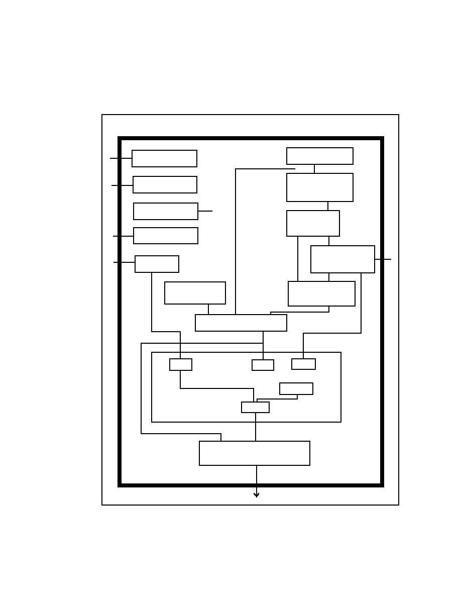
2.3 SCSP Chip Block Diagram
Figure 2.1 shows the SCSP chip block diagram.
SCSP
Sound CPU
Interface
Main CPU
Interface
DMA Transfer
Interface
MIDI
Interface
External
Input
Envolope
Generator
Level Calculator
LFO
Phase
Generator
Address
Pointer
Memory
Controller
Interpolator
AFLO PLFO
PHASE
PHASE
PLFO
ADSR-L ADSR-R
DATA DATA
ADSR-R
ADSR-L DATA
PCM-DATA
PCM_DATA
EG
ALFO
Output
Mixer
EXTS
MIXS
MEMS
EFREG
SEL
DSP
DIR
EFREG
EG
Figure 2.1 SCSP Chip Block Diagram
|

SEGA Confidential
14
Items shown in SCSP Chip Block Diagram Figure 2.1 are explained below.
Sound CPU Interface
Interface that connects to the MC68EC000.
Main CPU Interface
Interface that connects the system controller (SCU).
DMA Transfer Interface
This is the SCSP built-in DMA controller. It enables data
transfer between the SCSP and the sound memory.
MIDI Interface
This serial interface complies with MIDI specifications;
however, some external circuits will be needed to make it
compatible with a MIDI connector.
External Input (External Digital Audio Input Interface)
Interface that inputs a digital audio signal from an exter-
nal instrument (external device).
L F O (Low Frequency Oscillator)
Indicates a function generator that generates wave forms
of a frequency that is below the range that the human ear
can hear, and is used as a wave form for various modula-
tion.
Phase Generator
Block that calculates and outputs frequency data based
on
the sound generation frequency setting of the PCM
data.
Address Pointer
Creates the wave form address value based on the phase
information, etc., from the phase generator.
|

SEGA Confidential
Saturn SCSP User's Manual
15
Memory Controller
Block that outputs the address created by the address
pointer to the memory and reads data, etc.; it controls the
sound memory.
Interpolator
Block that interpolates the wave form data.
Envelope Generator (EG)
Functional calculation block that controls the sound
output level with time.
Level Calculator Block
Block that calculates the wave form output level based on
the level coefficient created by EG, TL (Total Level), and
ALFO.
DSP
Audio DSP that receives and holds the SCSP special
sound effects.
Output Mixer
Final block that contains functions that calculate various
positions and level adjustments needed to compile each
sound output in stereo.
|

SEGA Confidential
16
|

SEGA Confidential
Saturn SCSP User's Manual
17
Chapter 3
SCSP Functions
Chapter 3 Contents
3.1 Interface
18
Sound CPU Interface
18
Main CPU Interface
18
3.2 Memory Access Control
20
Chapter 3 Contents
3.1 Interface .......................................................
18
Sound CPU Interface .................................... 18
Main CPU Interface ...................................... 18
3.2 Memory Access Control ............................... 20
|
SEGA Confidential
18
3.1 Interface
The SCSP has two internal CPU (main CPU and sound CPU) interfaces. The main
CPU has higher priority than the sound CPU, so the processing speed of the sound
CPU depends on the operation of the main CPU.
Sound CPU Interface
The sound CPU interface is a block with specialized functions to enable it to connect
to the sound CPU. By adding this interface, the sound CPU can be directly con-
nected to the SCSP without external circuits.
Programs for the sound CPU reside in the sound memory. For this reason, all CPU
programs are placed in the sound CPU address space available.
Main CPU Interface
Access between the main CPU and the interface is shown in Figure 3.1.
SCU
D
A
DRAM
SCSP
MCD
MCCSN
MCRDYN
Address
Data
Figure 3.1 Access Overview
At the trailing edge of the select signal (MCCSN) from the main CPU, the interface is
started; at the leading edge of the select signal, the interface is ended. Also, when "1"
is output with respect to the ready signal (MCRDYN) to the main CPU, the select
signal (MCCSN) from the main CPU and the main CPU data bus (MCD[7:0]) do not
change.
|

SEGA Confidential
Saturn SCSP User's Manual
19
The following cautions should be observed with interfacing with the main CPU.
(1)
Because the main CPU cannot access in units of 8 bits, so read and write in 16
bit units.
(2)
When there is a request to read or write, the SCSP buffer gets the address and
data. Because of this, a "1" is output to the ready signal (MCRDYN) going to
the main CPU causing a wait. This wait continues until the internal processing
of the LSI is finished. For this reason, continuous read and writes that cause
many waits to occur should be avoided except when turning on the power.
(3)
When the power is turned on, the time necessary for initialization of sound
memory by continuous writing is approximately 100 msec for 4Mbit DRAM.
|
SEGA Confidential
20
3.2 Memory Access Control
When accessing sound memory from the SCSP, the following priorities are main-
tained.
1. PCM Data Read by PCM sound generator, accessed by DSP.
2. DRAM refresh cycle.
3. DMA transfer.
4. Access by the main CPU.
5. Access by the sound CPU.
When there is an access request with a high priority, there will be a wait state against
an access request with a low priority. Also, a high priority access request will not
occur while a low priority access is requested because the decision on which device
to be permitted to access memory (PCM sound generator block, DSP block, main
CPU, sound CPU, DMA, etc.) is made before any actual memory access is per-
formed.
CYCLE 0
CYCLE 1
CYCLE 2
CYCLE 3
High
Low
DSP
PCM
DSP
PCM
Access
Access
Access
Access
Refresh
cycle
Refresh
cycle
Refresh
cycle
Refresh
cycle
DMA
Access
DMA
Access
DMA
Access
DMA
Access
MCPU(SCU)
Access
MCPU(SCU)
Access
MCPU(SCU)
Access
MCPU(SCU)
Access
SCPU
Access
SCPU
Access
SCPU
Access
SCPU
Access
Memory Access
Priority
Figure 3.2 Memory Access Priorities
The performance of the SCSP / sound CPU is determined by the distribution of the
memory cycles.
There are 128 memory cycles within one sample (1/44.1K
=
22.68
µ
sec). These 128
cycles are distributed among the various devices. The number of times the CPU
accesses changes with the application, so there is no best way to access memory, but
be aware of the items on the following page.
|

SEGA Confidential
Saturn SCSP User's Manual
21
· Sound memory uses DRAM, so refresh cycles are required. In the Saturn sound
system, two empty cycles are required between each sample, so the number of
memory cycles that can be used by other devices is 126.
· The sound generator and DSP memory cycles have the highest priority memory
cycles.
· The sound generator uses two memory cycles to produce sound from one slot.
With a maximum of 32 slots, a total of 64 times of memory cycle may be used.
When the EG is at the maximum attenuation state ("3FF
H
"), the sound generator
does not access memory. Do KEY_OFF for those slots that are not producing
sound.
· The DSP accesses memory a maximum of 64 times. This changes with the DSP
application. Try to use the internal DSP registers as much as possible when
storing data temporarily.
· The sound CPU operating speed will decrease when using the SCSP built-in
DMA due to the extent of the wait state imposed on the sound CPU.
|

SEGA Confidential
22
|

SEGA Confidential
Saturn SCSP User's Manual
23
Chapter 4
SCSP Register
Chapter 4 Contents
4.1
Register Map
24
4.2
Sound Source Register
34
Loop Control Register
35
EG Register
40
FM Modulation Control Register
46
Using the FM Sound Generator Method
47
Sound Volume Register
72
PITCH Register
73
LFO Register
76
MIXER Register
80
Slot Status Register
89
Sound Memory Structure Register
89
MIDI Register
89
Timer Register
92
Interrupt Control Register
95
DMA Transfer Register
101
4.3
DSP Memory Control Register
103
Chapter 4 Contents
4.1
Register Map ..........................................................
24
4.2
Sound Source Register .......................................... 34
Loop Control Register ............................................ 35
EG Register ............................................................
40
FM Modulation Control Register ............................. 46
Using the FM Sound Generator Method ................ 47
Sound Volume Register ......................................... 72
PITCH Register ......................................................
73
LFO Register ..........................................................
76
MIXER Register .....................................................
80
Slot Status Register ...............................................
89
Sound Memory Structure Register ......................... 89
MIDI Register .........................................................
89
Timer Register ........................................................
92
Interrupt Control Register ....................................... 95
DMA Transfer Register ........................................... 101
4.3
DSP Memory Control Register ............................... 103
|
SEGA Confidential
24
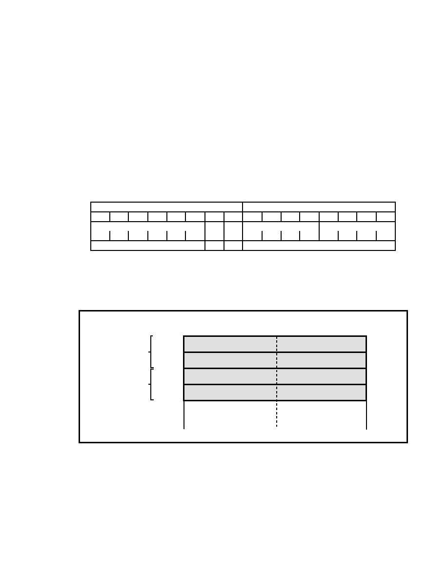
4.1 Register Map
The SCSP carries a wave form calculator unit called SLOT to realize FM sound
mixing.
Figure 4.1 describes the SCSP memory map and the allocation of the individual
registers that make up the memory map.
Individual Slot Control Register
( 5 0 8 W )
SCSP Common Control Register
( 2 4 W )
Sound Data Stack
( 6 4 W )
DSP Control Register
(1 0 1 0 W )
Note) W: Word = 16bit
100EE3
100700
10067F
100600
10042F
100400
1003F8
100000
H
H
H
H
H
H
H
H
Figure 4.1 SCSP Memory Map (1906W)
|
SEGA Confidential
Saturn SCSP User's Manual
25
The individual slot control register represents the allocation of the registers config-
ured in each of the 32 slots (SLOT0~SLOT31).
The location of bit allocation for each register is described as [3 : 0]. For example, SA
[19 : 16] represents the allocation from the 16th bit through the 19th bit of SA.
KX:KYONEX KB:KYONB 8B:PCM8B
HO:EGHOLD LS:LPSLNK SI:STWINH
SD:SDIR RE:LFORE
DISDL[2:0]
DIPAN[4:0]
EFSDL[2:0]
EFPAN[4:0]
ISEL[3:0]
IMXL[2:0]
ALFOS[2:0]
ALFOWS
PLFOS[2:0]
PLFOWS
LFOF[4:0]
RE
OCT[3:0]
FNS[9:0]
MDYSL[5:0]
MDXSL[5:0]
MDL[3:0]
SI
SD
TL[7:0]
RR[4:0]
DL[4:0]
KRS[3:0]
LS
D2R[4:0]
D1R[4:0]
HO
AR[4:0]
LEA[15:0]
LSA[15:0]
SA[15:0]
KX
KB
SBCTL
SSCTL
LPCTL
8B
SA[19:16]
00
18
H
H
Figure 4.2 Individual Slot Control Register
Table 4.1 Individual Slot Control Register (1)
Designation
Contents
KYONEX (KX)
Execute KEY_ON
KYONB (KB)
Record KEY_ON, KEY_OFF
SBCTL
Source bit control
SSCTL
Sound source control
LPCTL
Loop control
PCM8B (8B)
Select wave form data format
SA
Start address
LSA
Loop start address
|

SEGA Confidential
26
Table 4.2 Individual Slot Control Register (2)
LEA
Loop end address
D2R
Decay 2 rate
D1R
Decay 1 rate
EGHOLD (HO)
EG hold mode
AR
Attack rate
LPSLNK (LS)
Loop start link
KRS
Key rate scaling
DL
Decay level
RR
Release rate
STWINH (SI)
Stack write inhibit
SDIR (SD)
Sound direct
TL
Total level
MDL
Modulation level
MDXSL
Select modulation input X
MDYSL
Select modulation input Y
OCT
Octave
FNS
Frequency number switch
LFORE (RE)
LFO reset
LFOF
LFO frequency
PLFOWS
Select LFO frequency modulation wave form
PLFOS
LFO frequency modulation level
ALFOWS
Select LFO amplitude modulation wave form
ALFOS
LFO amplitude modulation level
ISEL
Input select
IMXL
Input mix level
DISDL
Direct data send level
DIPAN
Direct data, fixed position
EFSDL
Effect data send level
EFPAN
Effect data, fixed position
|
SEGA Confidential
Saturn SCSP User's Manual
27
Table 4.3 Individual Slot Control Register Address Map
Slot
Address
Slot
Address
0
100000
H
~ 100017
H
16
100200
H
~ 100217
H
1
100020
H
~ 100037
H
17
100220
H
~ 100237
H
2
100040
H
~ 100057
H
18
100240
H
~ 100257
H
3
100060
H
~ 100077
H
19
100260
H
~ 100277
H
4
100080
H
~ 100097
H
20
100280
H
~ 100297
H
5
1000A0
H
~ 1000B7
H
21
1002A0
H
~ 1002B7
H
6
1000C0
H
~ 1000D7
H
22
1002C0
H
~ 1002D7
H
7
1000E0
H
~ 1000F7
H
23
1002E0
H
~ 1002F7
H
8
100100
H
~ 100117
H
24
100300
H
~ 100317
H
9
100120
H
~ 100137
H
25
100320
H
~ 100337
H
10
100140
H
~ 100157
H
26
100340
H
~ 100357
H
11
100160
H
~ 100177
H
27
100360
H
~ 100377
H
12
100180
H
~ 100197
H
27
100380
H
~ 100397
H
13
1001A0
H
~ 1001B7
H
29
1003A0
H
~ 1003B7
H
14
1001C0
H
~ 1001D7
H
30
1003C0
H
~ 1003D7
H
15
1001E0
H
~ 1001F7
H
31
1003E0
H
~ 1003F7
H
|
SEGA Confidential
28
The SCSP control register allocates the interrupt register and timer register, etc., that
are commonly used.
Figure 4.3 SCSP Common Control Register
M4 DB MVOL[3:0]
RBL RBP[19:13]
OF OE IO IF IE MIBUF[7:0]
MOBUF[7:0]
DMEA[15:1]
DMEA[19:16] DRGA[11:1]
GA DI EX DTLG[11:1]
TACTL[2:0] TIMA[7:0]
TBCTL[2:0] TIMB[7:0]
TCCTL[2:0] TIMC[7:0]
SCIEB[10:0]
SCIPD[10:0]
SCIRE[10:0]
SCILV0[7:0]
SCILV1[7:0]
SCILV2[7:0]
MCIEB[10:0]
MCIPD[10:0]
MCIRE[10:0]
M4:MEM4MB DB:DAC18B OF:MOFULL
OE:MOEMP IO:MIOVF IF:MIFULL
IE:MIEMP GA:DGATE DI:DDIR
EX:DEXE
10042F
100430
H
H
10040F
100410
100409
10040A
100400
H
H
H
H
H
MSLC[4:0]
CA[3.0]
|
SEGA Confidential
Saturn SCSP User's Manual
29
Table 4.4 SCSP Common Control Register
Designation
Contents
MEM4MB (M4)
Memory size designation
DAC18B (DB)
Use the 18 bit D/A converter on the digital output
VER
Version number
MVOL
Master volume
RBL
Ring buffer length
RBP
Ring buffer lead address
MOFULL (OF)
Output FIFO is full
MOEMP (OE)
Output FIFO is empty
MIOVF (IO)
Input FIFO overflow
MIFULL (IF)
Input FIFO full
MIEMP (IE)
Input FIFO empty
MIBUF
MIDI input data buffer
MOBUF
MIDI output data buffer
MSLC
Monitor Slot
CA
Call Address
DMEA
DMA transfer start memory address
DRGA
DMA transfer start register address
DGATE (GA)
DMA transfer gate 0 clear
DDIR (DI)
DMA transfer direction
DEXE (EX)
DMA transfer start
DTLG
DMA transfer data count
TACTL
Timer A pre-scaler control
TIMA
Timer A count data
TBCTL
Timer B pre-scaler control
TIMB
Timer B count data
TCCTL
Timer C pre-scaler control
TIMC
Timer C count data
SCIEB
Allow sound CPU interrupt
SCIPD
Request sound CPU interrupt
SCIRE
Reset sound CPU interrupt
SCILV0
Sound CPU interrupt level bit0
SCILV1
Sound CPU interrupt level bit1
SCILV2
Sound CPU interrupt level bit2
MCIEB
Allow main CPU interrupt
MCIPD
Request main CPU interrupt
MCIRE
Reset main CPU interrupt
|
SEGA Confidential
30
The sound data stack is where sound data is stored. Sound data is in two generation
configuration (GENERATION A and B). Each generation can control up to 32 sound
data.
DIRECT SOUND SLOT DATA STACK (GENERATION A) "SOUS[15:0]"
DIRECT SOUND SLOT DATA STACK (GENERATION A) "SOUS[15:0]"
DIRECT SOUND SLOT DATA STACK (GENERATION B) "SOUS[15:0]"
DIRECT SOUND SLOT DATA STACK (GENERATION B) "SOUS[15:0]"
100600
10063F
100640
10067F
(32W)
(32W)
H
H
H
H
Figure 4.4 Sound Data Stack
Table 4.5 Sound Data Stack
Designation
Contents
SOUS
Sound stack
|

SEGA Confidential
Saturn SCSP User's Manual
31
On the DSP control register, the interface block area of DSP is defined which is built
within SCSP.
COEF REG "COEF[12:0]"
O
O
O
O O 0
COEF REG "COEF[12:0]"
MEMORY ADDRESS REG "MADRS[16:1]"
MEMORY ADDRESS REG "MADRS[16:1]"
DSP MICRO PROGRAM
DSP INTERNAL BUFFER
100700
(64W)
10077F
100780
(32W)
1007BF
100800
(512W)
100BFF
100C00
(370W)
100EE3
H
H
H
H
H
H
H
H
Figure 4.5 DSP Control Register
Table 4.6 DSP Control Register
Designation
Contents
COEF
DSP coefficient buffer
MADRS
Memory address register
|
SEGA Confidential
32
512W
DSP MICRO PROGRAM (STEP_127) "MPRO[15:0]"
DSP MICRO PROGRAM (STEP_127) "MPRO[31:16]"
DSP MICRO PROGRAM (STEP_127) "MPRO[47:32]"
DSP MICRO PROGRAM (STEP_127) "MPRO[63:48]"
DSP MICRO PROGRAM (STEP_126) "MPRO[15:0]"
DSP MICRO PROGRAM (STEP_1) "MPRO[63:48]"
DSP MICRO PROGRAM (STEP_0) "MPR0[15:0]"
DSP MICRO PROGRAM (STEP_0) "MPRO[31:16]"
DSP MICRO PROGRAM (STEP_0) "MPRO[47:32]"
DSP MICRO PROGRAM (STEP_0) "MPRO[63:48]"
100800
100807
100808
100BF8
100BFF
H
H
H
H
H
Figure 4.6 DSP Micro Program Map
Table 4.7 DSP Micro Program
Designation
Contents
MPRO
Micro program register
|
SEGA Confidential
Saturn SCSP User's Manual
33
Figure 4.7 DSP Internal Buffer Map
"TEMP[7:0]"
WORK BUFFER 00 "TEMP[23:8]"
"TEMP[7:0]"
WORK BUFFER 127 "TEMP[23:8]"
MEMS[7:0]"
"
SOUND MEMORY 00 "MEMS[23:8]"
"MEMS[7:0]"
SOUND MEMORY 31 "MEMS[23:8]"
"MIXS[3:0]"
MIX SOUND SLOT DATA STACK 00 "MIXS[19:4]"
"MIXS[3:0]"
MIX SOUND SLOT DATA STACK 15 "MIXS[19:4]"
EFFECTED DATA OUTPUT 00 "EFREG[15:0]"
EFFECTED DATA OUTPUT 15 "EFREG[15:0]"
100EE3
100EDF
100EE0
(16W)
100EBF
100EC0
(32W)
100E7F
100E80
(64W)
100DFF
100E00
(256W)
100C00
H
H
H
H
H
H
H
H
H
H
Table 4.8 DSP Internal Buffer
Designation
Contents
TEMP
DSP temporary (universal) buffer
MEMS
Memory data stack
MIXS
Mix stack
EFREG
Effect register
|
SEGA Confidential
34
4.2
Sound Source Register
The sound source (block) register is made up of the allocations shown in Table 4.9.
Table 4.9 Sound Source (Block) Register Allocation
Register Name
Bit Name
Loop Control Register
KYONEX, KYONB, SBCTL, SSCTL, SA, LSA,
LEA, PCM8B, LPCTL
EG Register
EGHOLD, AR, D1R, D2R, RR, DL, KRS, LPSLNK
FM Modulation Control Register
SOUS, MDL, MDXSL, MDYSL, STWINH
Sound Volume Register
TL, SDIR
PITCH Register
OCT, FNS
LFO Register
LFORE, LFOF, ALFOWS, ALFOS,
PLFOWS,PLFOS
MIXER Register
IMXL, ISEL, DISDL, DIPAN, EFSDL, EFPAN,
MVOL, DAC18B
Slot Status Register
MSLC, CA
Sound Memory Config. Register
MEM4MB
MIDI Register
MIBUF, MIOVF, MIFULL, MIEMP, MOFULL,
MOEMP, MOBUF
Timer Register
TACTL, TIMA,TBCTL, TIMB, TCCTL, TIMC
Interrupt Control Register
SCIPD, SCIEB, SCIRE, SCILVO, SCILV1, SCILV2,
MCIPD, MCIEB, MCIRE
DMA Transfer Register
DGATE, DDIR, DEXE, DMEA, DRGA,DTLG
|
SEGA Confidential
Saturn SCSP User's Manual
35
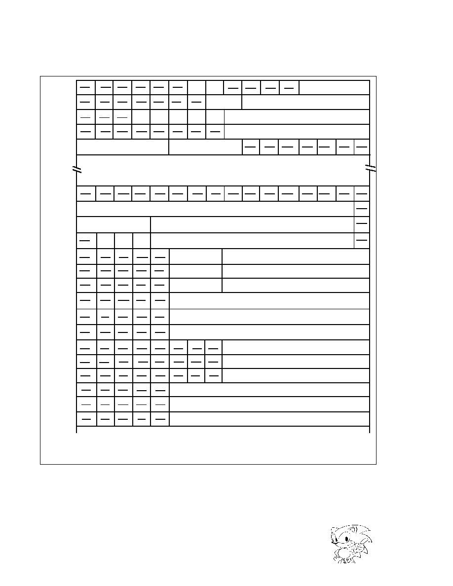
Below is the definition of the bit in terms of the sound generator block register,
based on the classifications in Table 4.9. The symbols following the register names
have the following meanings: (R) read only, (W) write only, (R/W) both read and
write are possible.
When reading data from the write only register (bit), that value becomes "0
B
".
When writing data to the read only register (bit), always write "0
B
".
Loop Control Register
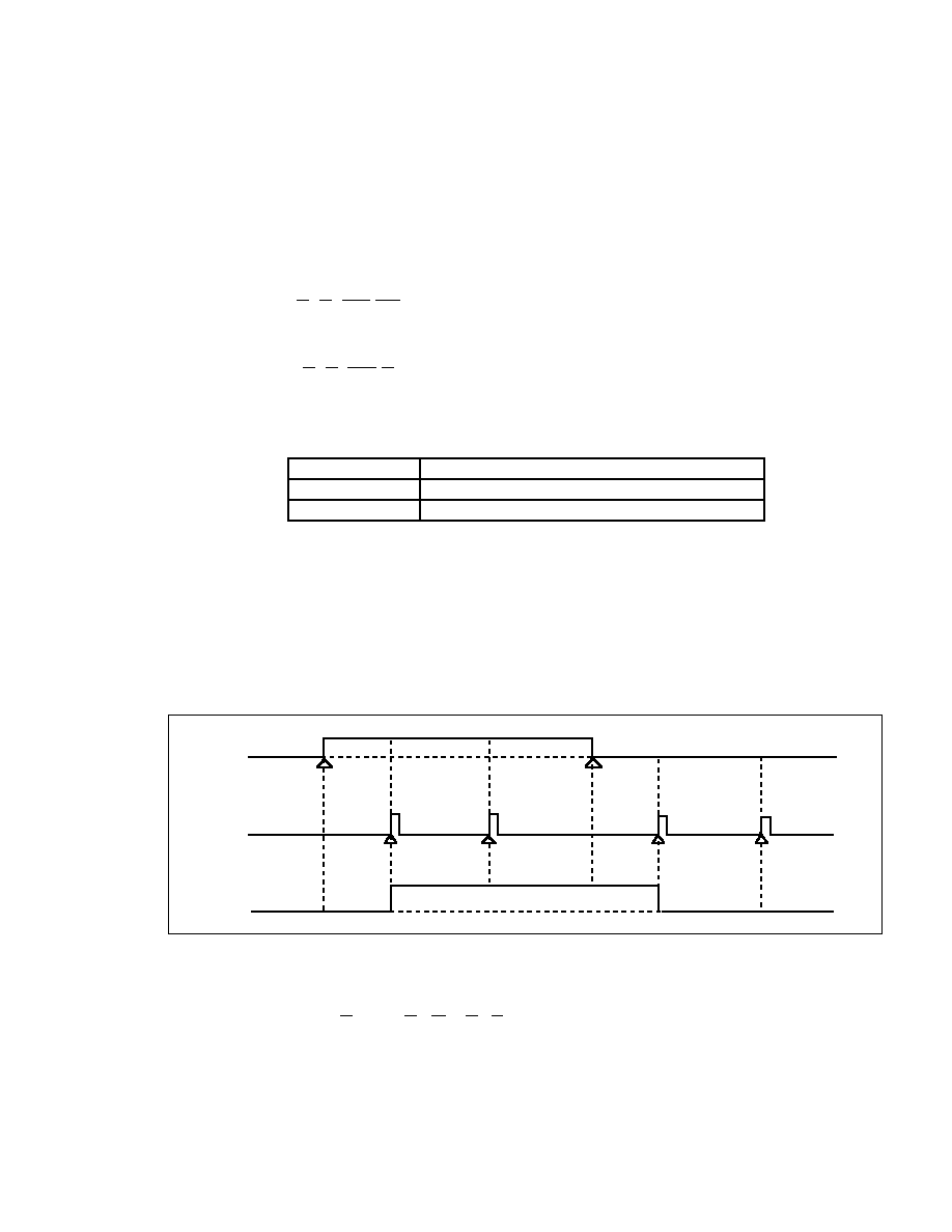
KYONEX (W) ;KeY_ON EXecution
A "1B" written here will execute KEY_ON, OFF for all of the slots.
KYONB (R/W) ;KeY_ON Bit
Registers KEY_ON,OFF. (If you wish to KEY_ON simultaneously, the "KYONB" of
the slot you want to turn ON must be set to "1B".)
Table 4.10 KYONB Function
"KYONEX" and "KYONB" exist in each slot. The sequence of KEY_ON and
KEY_OFF is shown in Figure 4.8.
There is no need to write a "0B" in "KYONEX" after writing a "1B". Also a "1B" in
"KYONEX" is used for all slots, so you don't need to set to "1B" per a specific slot.
KYONB
REGISTER
KYONEX
REGISTER
KEYON
TRIGGER
"0"
"0"
"0"
"0"
"0"
"0"
"0"
"0"
"0"
"0"
"0"
"1"
"1"
"OFF"
"ON"
"ON"
"ON"
"OFF"
"1" WRITE
"1" WRITE
"1"WRITE
"1"WRITE
Time
Time
Time
Execute
Ignore
Execute
No Meaning
ON
OFF
"1"
"1"
"1"
"1"
"1" WRITE
"0" WRITE
"1"
Figure 4.8 KEY_ON and KEY_OFF Sequence
SBCTL[1:0] (R/W) ;Source Bit ConTroL
Specifies bit reversal operation of the sound input data. The reversal function be-
comes valid for bits with "1B" written to them.
bit
Function
0
Registers KEY_OFF
1
Registers KEY_ON
|
SEGA Confidential
36
Table 4.11 SBCTL Function
SSCTL[1:0] (R/W) ;Sound Source ConTroL
Designates the data to be used as sound input data. When using the wave form data
in sound memory to produce a sound, write "0B". When this register is "1
B
", the
slot with respect to which setting has been applied (the LFO accompanied with each
slot) will output noise.
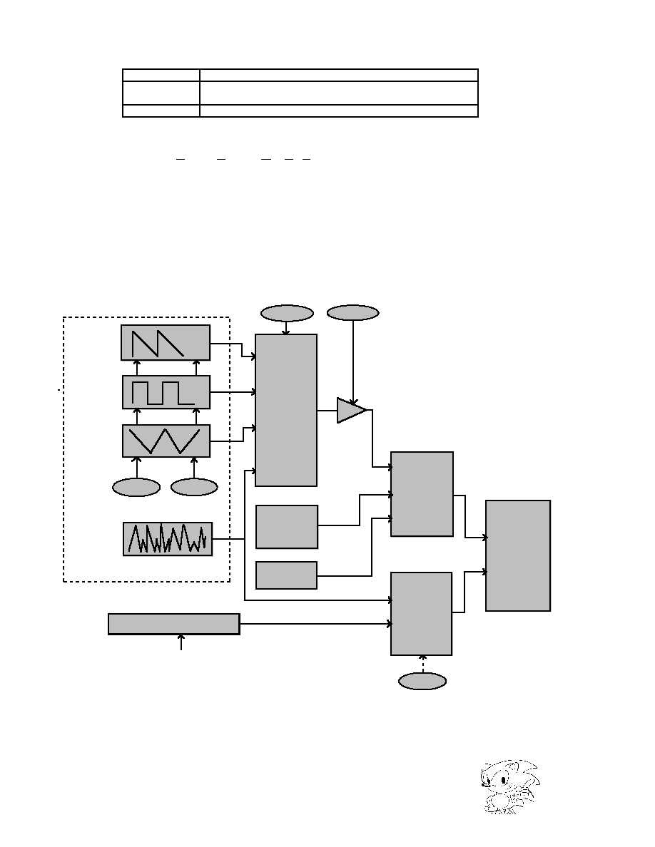
The block diagram of noise generated when "SSCTL"="1
B
" and the relation to LFO
is shown with ALFO added in Figure 4.9
ALFOWS
SLOT
Wave Form Data
Buffer
TL
EG
SSCTL
SELECTOR
2
TO
1
Waveform Data From
Wave Form Memory (RAM)
Normal Sound
Noise
White Noise
Sound Data
Noise On/Off
Function
Level
Calculater
Block
Level
Coefficient
Level
Coeffici-
ent
Calculater
Block
LFORE
LFOF
Amplitude Modulation Rate
Adjustment
* Alfo is Attached Here
ALFOS
SELECTOR
4
TO
1
LEO Waveform Generator
Sawtooth
Wave
Square
Wave
Triangle
Wave
ALFOWS
Figure 4.9 Relation of the Noise Generation Block Diagram and LFO
Bit
Function
SBCTL0
Reverse selection for bits other than the source wave form
data sign bit.
SBCTL1
Reverse selection for the source wave form data sign bit.
|
SEGA Confidential
Saturn SCSP User's Manual
37
Each slot utilizes the LFO noise oscillator output to output noise. Here, the LFO
parameters in Figure 4.9 ("LFORE", "LFOF", "ALFOWS", "ALFOS", "PLFOWS",
"PLFOS") will not affect noise as voice data.
Also, when using LFO in low-frequency modulation with the LFO wave form selec-
tion at noise (ALFOWS="3H", or PLFOWS="3H") as in Figure 4.9, reset with the
"LFORE" will not function. The frequency also cannot be changed. This means that
when selecting noise, the LFO can select wave form but cannot change in terms of
other parameters.
Table 4.12 SSCTL Internal Configuration
SA[19:0] (R/W) ;Start Address
Specifies the waveform data start address in byte address when using memory
waveform data to generate sound. However, if the waveform data is "16 bit PCM"
("PCM8B"="0"), always set the register's lsb (SA0) to "0B".
LSA[15:0] (R/W) ; Loop Start Address
Represents the sound data loop start address in sample count from the "SA".
LEA[15:0] (R/W) ; Loop End Address
Represents the sound data loop end address in sample count from the "SA".
PCM8B (R/W) ; PCM 8Bit
Designates the format of the wave form data.
Table 4.13 Types of Sound Data
SSCTL
Data Used
0
External DRAM data
1
Internally generated data (noise)
2
Internally generated data (ALL "0")
3
Cannot be used
PCM8B
Sound Data
0
16Bit PCM data 2'S complement
1
8Bit PCM data 2'S complement
|
SEGA Confidential
38
LPCTL[1:0] (R/W) LooP ConTroL
Sets the loop format.
Table 4.14 Types of Loops
Loop processing or sound memory access will end with either of the following two
conditions:
(1)
After release, when the attenuation volume reaches maximum, or
(2)
When the loop is OFF, and the read point reaches the loop end point.
When using normal or reverse loops, set the data corresponding to
"SA+LSA" (loop start address) and the "SA+LEA" (loop end address) to the
same value. Using the same method with the alternative loop can make the
pitch the same as the normal or reverse loops.
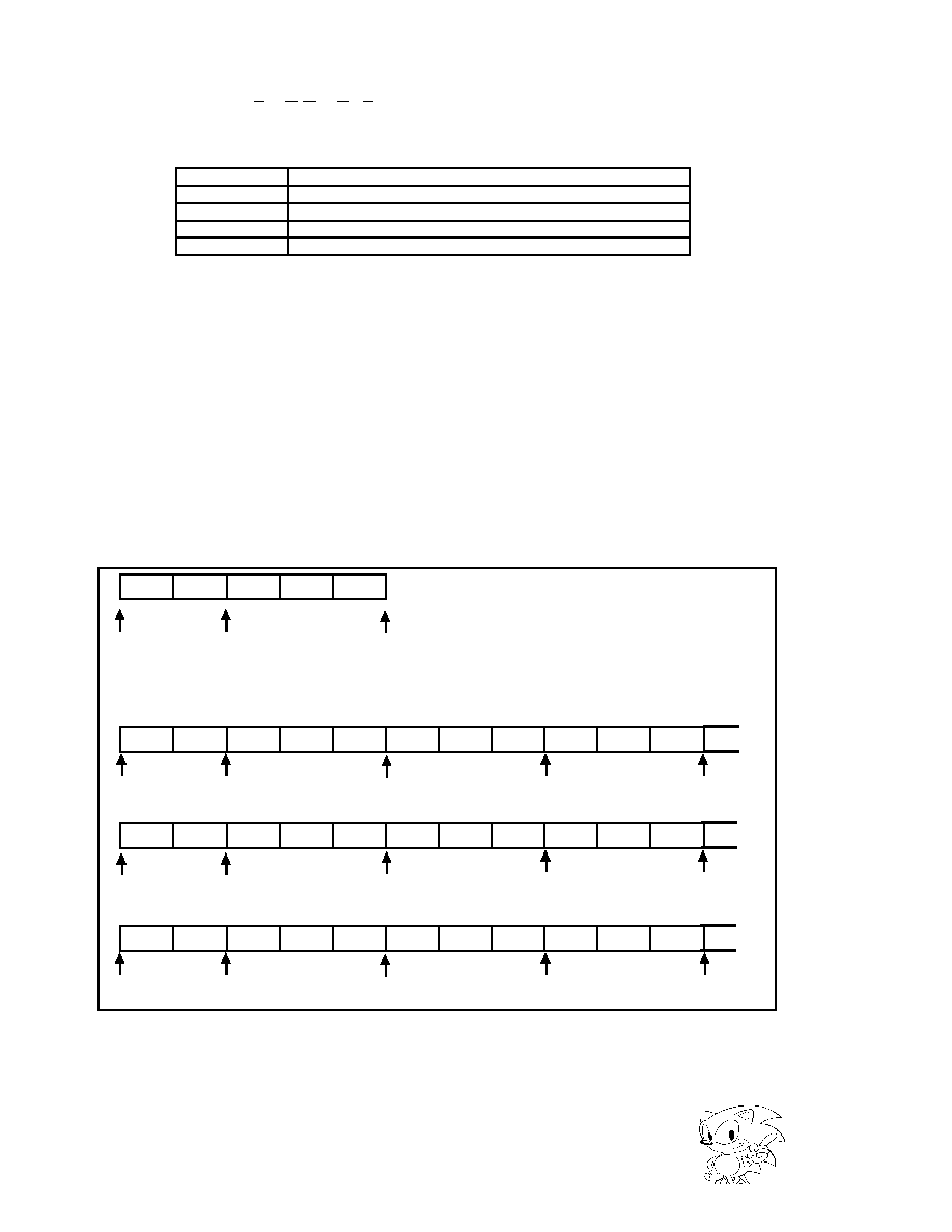
Figure 4.10 shows specific examples of loop types.
Attack Data
Loop Data
Using the sounds "ha- hi- hu- he- ho" as wave form data, the following sounds are produced when the
start address (SA), loop start address (LSA), and loop end address (LEA) are set as shown above.
haaaa
h i i i i huuuu
heeee
hoooo
SA
LSA
LEA
Normal Loop
haaaa
h i i i i huuuu
heeee
hoooo huuuu
heeee
hoooo huuuu
heeee
hoooo huu
q
Reversal Loop
haaaa
h i i i i
q
ooooh eeeeh
uuuuh
ooooh eeeeh
uuuuh
ooooh eeeeh
uuuuh ooo
Alternative Loop
haaaa
h i i i i
q
huuuu
heeee
hoooo ooooh eeeeh
uuuuh
heeee
hoooo ooo
huuuu
SA
SA
SA
LSA
LSA
LEA
LEA
LEA
LSA
LEA(LSA)
LEA(LSA)
LEA(LSA)
LSA(LEA)
LSA(LEA)
LSA(LEA)
Figure 4.10 Loop Types
LPCTL
Loop Format
0
Loop OFF
1
Normal loop
2
Reverse loop
3
Alternative loop
|

SEGA Confidential
Saturn SCSP User's Manual
39
The wave form for each of the normal loop, reversal loop and the alternative loop
can be represented as in figure 4.11. Note that the uuuu, eeee, oooo wave forms are
reversed from huuh, heeh, hooh wave forms.
Attack
Data
Normal Loop
Reversal Loop
Alternative Loop
Attack
Data
Attack
Data
The wave form for each of "huuu, heee, hooo" are defined as shown
below.
Figure 4.11 Loop Wave Forms
|
SEGA Confidential
40
EG Register
EG represents the change occurred by sound attenuation time, and has the following
four states.
· Attack State (Attack segment)
Indicates the start of the sound (start up).
· Decay 1 state (Decay 1 segment)
Indicates attenuation from the maximum volume.
· Decay 2 state (Decay 2 segment)
Indicates attenuation even lower than decay 1.
However, if DR2 is set to "0", the sound is maintained rather than attenuated.
· Release state (Release segment)
Indicates the attenuation until the sound disappears after KEY_OFF.
However, in all cases of sound generation state, EG does not necessarily go through
all four states. Depending on the timing of KEY_OFF various envelope curves are
drawn. An example is shown below.
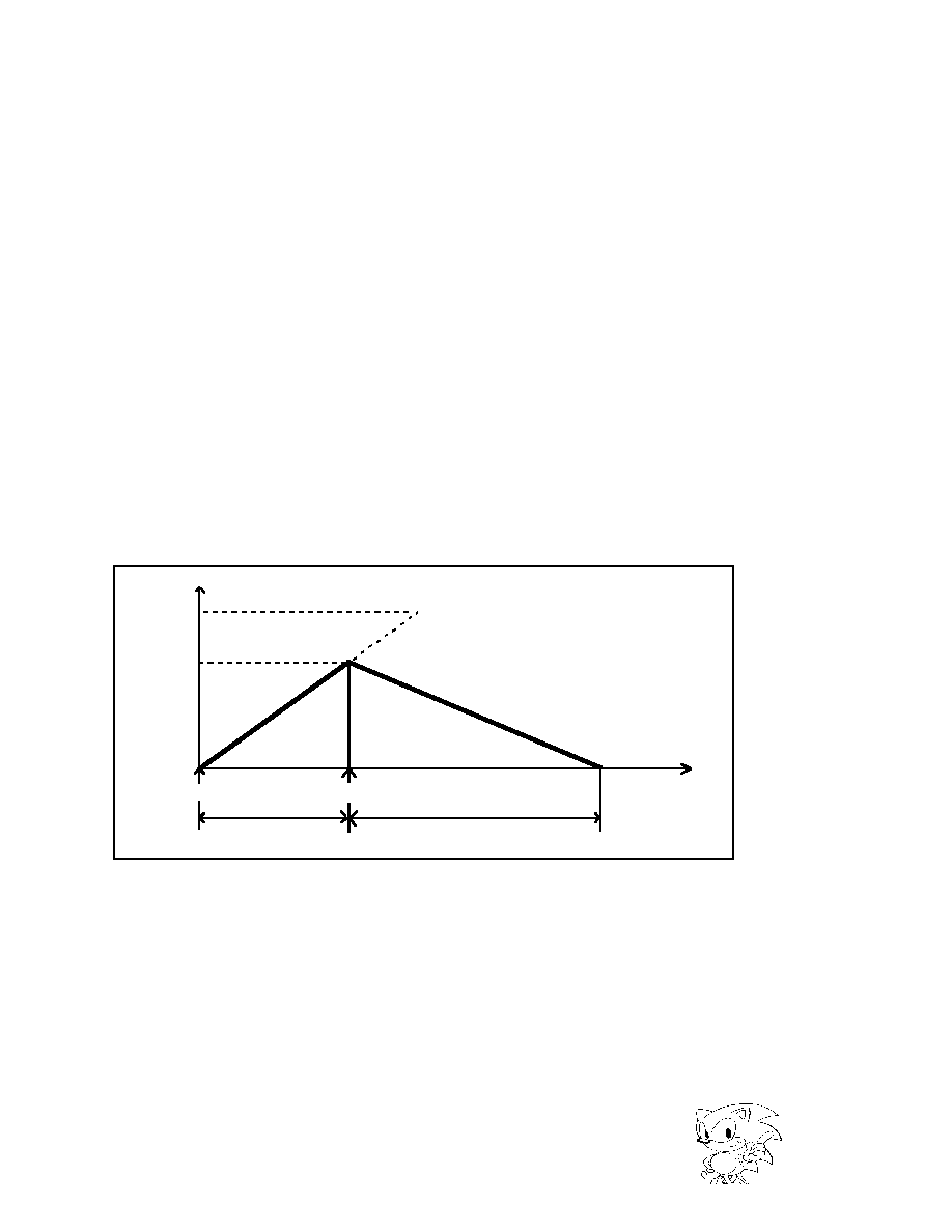
(a)
When KEY_OFF is executed during attack state transition
(Figure 4.12).
EG
000
3FF
KEY-ON
KEY-OFF
Time
KEY-OFF
LEVEL
Attack State
Release State
H
H
Figure 4.12 KEY_OFF During Attack State Transition
When KEY_OFF is executed, from that level (KEY_OFF LEVEL) the
sound is attenuated following the release rate ("RR") setting.
Therefore, in this case, the envelope curve skips the decay 1 and
decay 2 states. In this case, EG value does not reach "000
H
", rather,
with KEY_OFF as a turning point, it increases to "3FF
H
".
|
SEGA Confidential
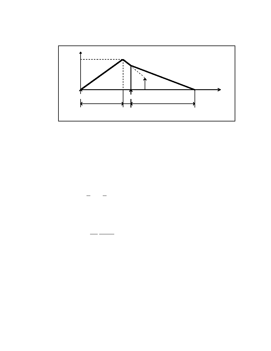
(b) When KEY_OFF is executed during decay 1 segment transition.
(Figure 4.13).
EG
000
3FF
KEY-ON
KEY-OFF
Time
DL
KEY-OFF
LEVEL
Attack State
Decay 1 State
Release State
H
H
Figure 4.13 KEY_OFF During Decay State Transition
When the decay 1 state starts, it attenuates towards the DL (decay
level) following the D1R (decay 1 rate) set value.
If KEY_OFF is executed during the above operation, the sound starts
to attenuate from the level KEY_OFF was executed (KEY_OFF
LEVEL) according to the value set in RR (release rate).
AR[4:0] (R/W) ; Attack Rate
Designates the change volume of EG in the attack state. When
"AR"="00H", the change volume (level attenuation volume) is
minimum (0). When "AR"="1FH", the change volume (level attenua-
tion volume) is maximum (MAX).
EGHOLD (R/W) EG HOLD mode
Designates whether to maintain or change the attack value. As shown
in Figure 4.12, when this bit is "1B" the attack value is held at "000H".
Also when this bit is "0B", it changes according to the value designated
by the AR register. In the hold mode, the time that EG retains "000H"
(time until it reaches segment 2) is determined by the "AR" value.
Saturn SCSP User's Manual
41
|
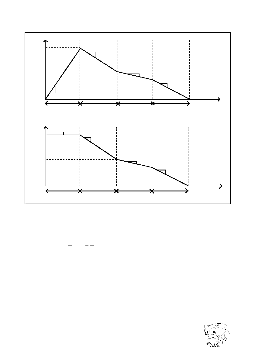
SEGA Confidential
When EGHOLD=1
EG
Time
Attack
State
Decay 1
State
Decay 2
State
Release
State
EG
When EGHOLD=0
Time
Attack
State
Decay 1
State
Decay 2
State
Release
State
000H
DL[4:0]
3FFH
000H
DL[4:0]
3FFH
D1R[4:0]
D2R[4:0]
RR[4:0]
AR[4:0]
D1R[4:0]
D2R[4:0]
RR[4:0]
AR[4:0]
Figure 4.14 Change in the Attenuation Volume
D1R[4:0] (R/W) ; Decay-1 Rate
Designates the EG change volume in the decay 1 state. When
"D1R"="00H", the change volume (level attenuation volume) is
minimum (0). When "D1R"="1FH", the change volume (level
attenuation volume) is maximum (MAX).
D2R[4:0] (R/W) ; Decay-2 Rate
Designates the EG change volume in the decay 2 state.When
"D2R"="00H", the change volume (level attenuation volume) is
minimum (0). When "D2R"="1FH", the change volume (level
attenuation volume) is maximum (MAX).
42
|

SEGA Confidential
RR[4:0] (R/W) ; Release Rate
Designates the change volume of the EG in the release state.
When "RR"="00H", the change volume (level attenuation
volume) is minimum (0). When "RR"="1FH", the change
volume (level attenuation volume) is maximum (MAX).
DL{4:0] (R/W) ; Decay Level
Designates the upper 5 bit of the attenuation level (EG) that
moves from decay 1 state to decay 2 state. When the upper
decay 1 state attenuation level upper 5 bits match the DL value,
the state moves to decay state 2. When "DL"="00H", the level
is maximum (MAX). When "DL"="1F
H
", the level is minimum
(MIN).
KRS[3:0] (R/W) Key Rate Scaling
Designates the level of EG key rate scaling condition. 00H
indicates minimum scaling; 0EH designates maximum scaling.
When set to 0FH, it designates that scaling OFF.
LPSLNK (R/W) ; LooP Start LiNK
The function of the "LPSLNK" (loop start link) is to synchronize
the transition to decay 1 state from the loop start and EG attack
states.
When "LPSLNK" ="0" there is no relation between the EG state
transition and the loop start point position. When "LPSLNK"
="1", the following two changes can be seen.
1) When, in terms of time, EG reaches "000
H
" in the attack state faster than when
the wave form read address reaches the loop start point ("SA"+"LSA") (Figure
4.15). In this case, EG will reach the MAX level first (P.1). However, since
moving to the next segment is not possible (decay 1 state) until the wave form
read address reaches the loop start point, EG is maintained at MAX level. Next,
when the wave form read address reaches the loop start point (P.2) EG will move
to the decay 1 state.
Saturn SCSP User's Manual
43
|
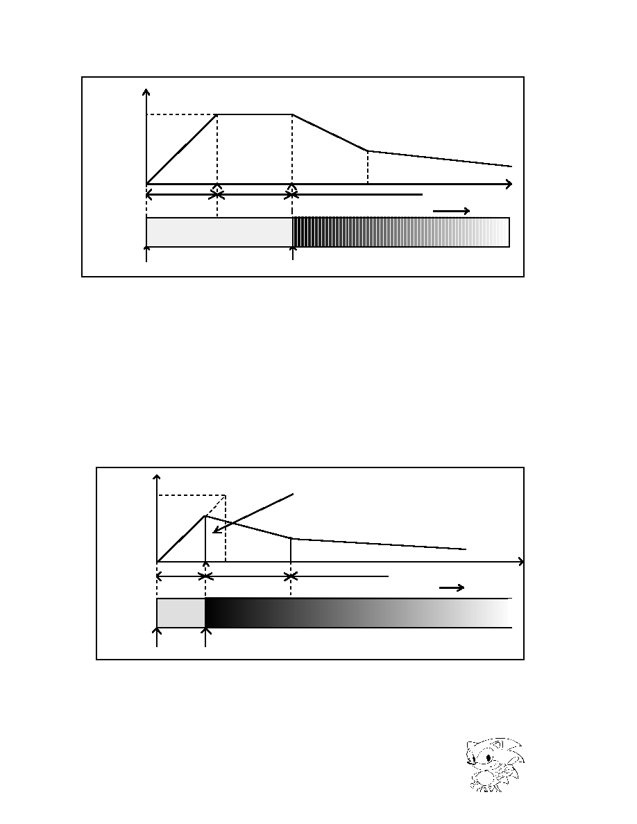
SEGA Confidential
EG
DL
ADDRESS
SA LSP (SA+LSA) :LOOP START POINT
000
3FF
P.1
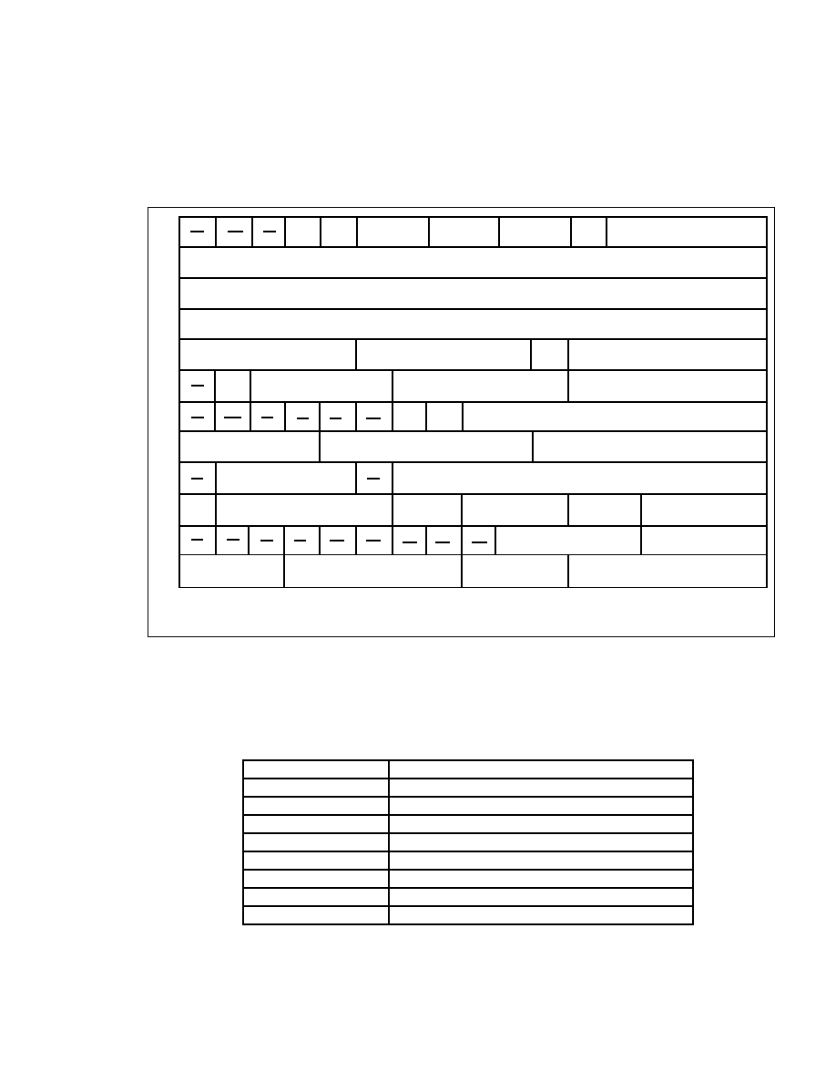
P.2
Wave Form
Data
Attack
State
Decay 1
State
Time
EG
H
H
Attack
State
Figure 4.15 Transition (1) from the Attack State to Decay 1
2) In terms of time, EG reaches "000
H
" in the attack state slower than when the
wave form read address reaches the loop start point ("SA"+"LSA").
This pattern has an additional two patterns.
- When the wave form read address reaches the loop start point, and the "SCL"
at this point (EG level) is larger than the "DL" (decay level) (reversed when
compared to the actual EG level). (Figure 4.16)
SA LSP (SA+LSA) :LOOP START POINT
Wave Form
Data
3FF
000
EG
P.
1
P.2
DL
SCL>DL
Time
ADDRESS
Attack
State
Decay 1
State
Decay 2
State
SCL: SEGMENT CHANGE LEVEL
EG
H
H
Figure 4.16 Transition (2) from the Attack State to Decay 1
44
|

SEGA Confidential
After the wave form read address reaches the loop start point, the EG will shift to
the decay 1 state (P.1). Next, when the EG value reaches the DL (decay level), it will
shift to the decay 2 state (P.2).
- When the wave form read address reaches the loop start point, and the "SCL"
at this point (EG level) is smaller than the "DL" (decay level) (reversed when
compared to the actual EG level). (Figure 4.17)
EG
000
3FF
P.1
DL
SCL<DL (SCL=DL)
SCL: SEGMENT CHANGE LEVEL
Time
ADDRESS
Decay 1
Status
Wave Form
Data
SA LSP (SA+LSA) :LOOP START POINT
EG
H
H
Figure 4.17 Transition (3) from the Attack State to Decay 1
After the wave form read address reaches the loop start point, the EG will shift to
the decay 1 state (P.1). After this, since the EG value will no longer reach the
"DL" (decay level), it will continue to retain level 0 (EG value is "3FFH") with-
out moving to decay 2 state.
Saturn SCSP User's Manual
45
|
SEGA Confidential
FM Modulation Control Register
SOUS[15:0] (R/W) ; SOUnd Stack
This is a data buffer for a slot output. It is a 64 word ring buffer
that can hold two generations of sampling data. This is used in
addition to processing between slots and modulation.
MDL[3:0] (R/W) ; MoDuLation level
Specifies the effects (modulation rate) of modulation to the
modulation input source.
Table 4.15 Modulation Rate According to the Register Set Value
MDXSL[5:0] (R/W) ; MoDulation input-X SeLect
Designates the source to be used as modulation input X. The
modulation input X source slot is specified by two complimen-
tary numbers showing the relative number from the current
slot. Also, when this value is within the range "1C
H
" to 3B
H
" it
shows the latest generation; if out of range it shows one sample
past the latest generation. (See Table 4.16)
MDYSL[5:0] (R/W) ; MoDulation input-Y SeLect
Designates the source to be used as modulation input Y. The
modulator input Y source slot is indicated by two complimen-
tary numbers showing the relative number from the current
slot. Also, when this value is within the range of "1C
H
" to 3B
H
"
it represents the latest generation; if out of range it represents 1
sample past the latest generation. (See Table 4.16)
STWINH (R/W) ; STack Write INHibit
When this bit is "1B", writing the slot output to the direct data
stack ("SOUS") is inhibited. Normally "0B" is fine.
MDL [3:0]
0 ~ 4
5
6
7
8
9
A
B
C
D
E
F
Modulation Rate (
±
n
)
0
1/16
1/8
1/4
1/2
1
2
4
8
16
32
64
46
|
SEGA Confidential
Using the FM Sound Generator Method
The FM sound generator method is a method in which modulation is performed by
adding different wave form generator output to the wave form generator phase
input. FM voice mixing is accomplished by a wave form calculator unit called a slot.
Figure 4.18 shows a block diagram of a slot.
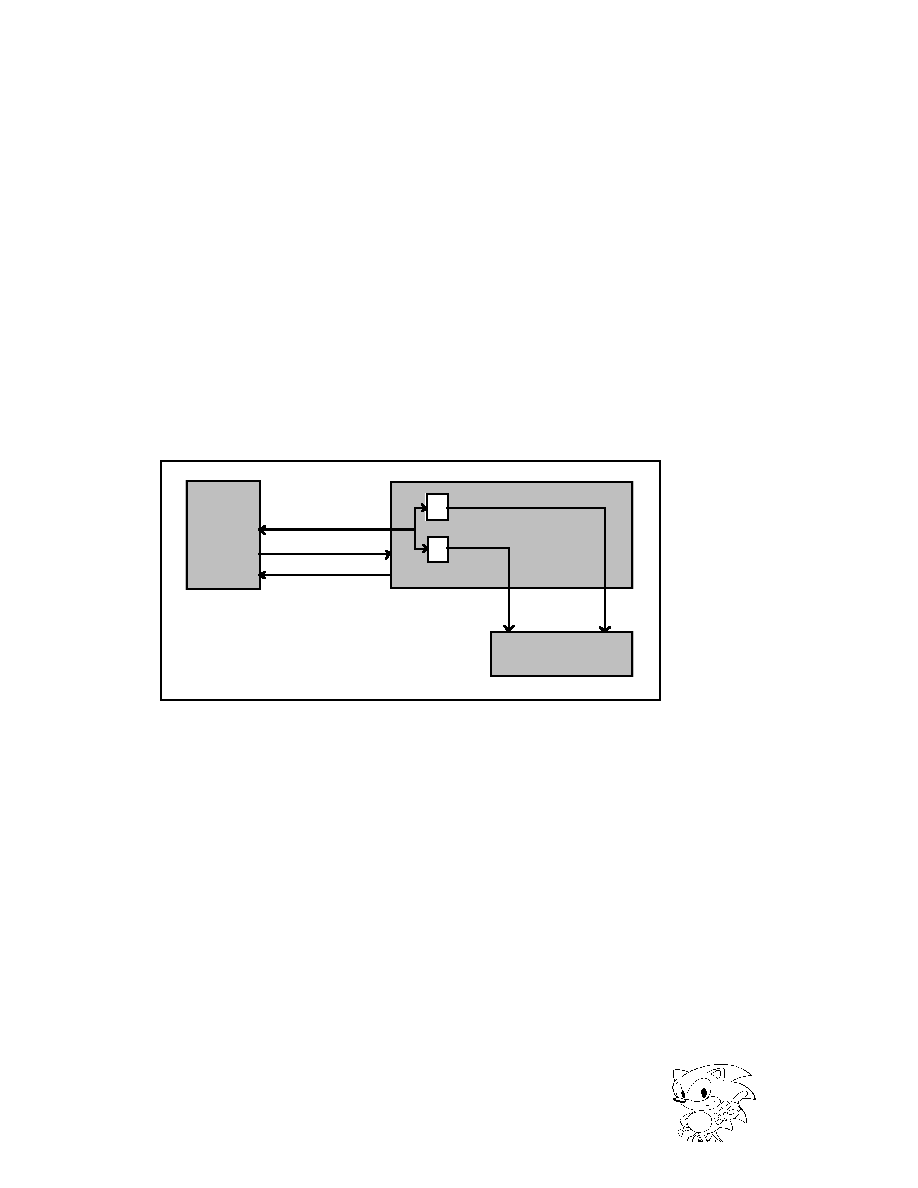
P L F O
P G
SOUND
STACK
DATA
SOUND
STACK
DATA
Averaging Operation
Unit
Waveform Phase
Value
PHASE ADDER
Waveform RAM
MEMORY ADDRESS
WAVE DATA
Waveform
Address
Pointer
Waveform
Data
Buffer
A L F O
E G
Level Coefficient
(Volume)
Waveform Level
Calculation
Output to DIRECT & DSP SLOT OUTPUT
Figure 4.18 SLOT Block Diagram
Saturn SCSP User's Manual
47
|
SEGA Confidential
To output a sound from a slot, wave form data required to run the slot is written to
the wave form RAM. Sound is started by the wave form read address, loop start
address, loop end address, sound pitch, sound level, setting the various EG settings,
and turning KEY_ON. SCSP operates as one large cycle of 22.68[
µ
sec] as a whole.
The PG (Phase Generator) controls the reading rate of the waveform, which is deter-
mined by the sound generation frequency setting. As long as the sound frequency
isn't changed, the PG creates a fixed value per 1Fs cycle (22.68[
µ
sec] = 1/44.1KHz),
and it does a cumulative addition per Fs cycle and outputs. As shown in Figure
4.19, this is added to each address pointer. The resulting values are output to the
address bus as wave form address and the wave form data in RAM corresponding
to those wave form addresses are read.
Address Output
P G
X SOUS
Modulation
Operation Unit
Averaging
Operation Unit
Y SOUS
Phase Adder
Adder/
Subtractor
Coincidence/
Comparitor Circuit
Coincidence/
Comparitor Circuit
ADDRESS
POINTER
MDL
S A
LSA
LEA
TIME
Amplitude
(Wave Form on the
Wave Form RAM)
(Address Pointer
Output Value)
(Wave Form Readout
Value)
Wave Form
ADDRESS
Time / Phase
Correlation
Figure 4.19 Wave Form Address Generator
Figure 4.20 Creating Wave Form Addresses and Reading Wave Form Data
48
|
SEGA Confidential
When the oscillation frequency is constant (PG internal generations are constant for
all Fs cycles), the address pointer output becomes a straight line (as shown in Figure
4.20), and can be read without changing wave form on the wave form RAM.
The address pointer may appear to be a straight line, but because calculations are
performed per 1Fs cycle, they will create a line like the stairs shown in Figure 4.21.
These steps become the PG internal generator value.
WAVE
ADDRESS
PG Internally
generated value.
TIME
Each 22.68
sec intervals
µ
Figure 4.21 Expanded Address Pointer Output Diagram
If the frequency is increased, the PG creation value will increase, causing sharp slope
for the PG output and address pointer output value (function).
On the other hand, if the frequency is decreased, the PG creation value will be re-
duced, causing a softer slope for the PG output value and address pointer output
value (function) as shown in Figure 4.22.
Saturn SCSP User's Manual
49
|

SEGA Confidential
Amplitude
· If the frequency
is increased
Wave Form
ADDRESS
Time Phase Correlation
(Wave Form in the
Wave Form RAM)
(Wave form read value)
(Output value of the
address pointer)
(Wave form read value)
(Wave Form in the
Wave Form RAM)
(Output value of the
address pointer)
Amplitude
Time Phase Correlation
Wave Form
ADDRESS
· If the frequency
is decreased.
Figure 4.22 Frequency Address Pointer Output Value
When FM voice mixing is performed, short cycle wave forms are looped. Therefore,
the output value (function) of the address pointer is similar to Figure 4.23 below.
Amplitude
Wave Form
ADDRESS
(Output value of the address pointer)
(Wave form read value)
TIME
(Wave Form in the
Wave Form RAM)
Loop Start Address (LSA)
a: Start Address (SA)
b: Loop End Address (LEA)
Address Pointer Output
(Phase)
RAM
Data
Figure 4.23 Address Pointer Output Value During FM Voice Mixing Execution(1)
50
|
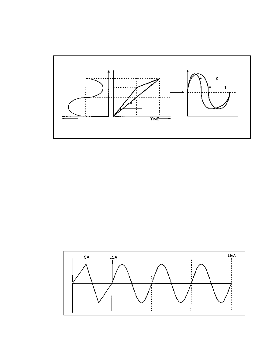
SEGA Confidential
The start address is set in address "a", while the loop start address is set to "0000H".
The wave form read address and the wave form loop start address are both set to the
same address. Furthermore, the "b" address is set with the loop end address, so it
becomes the wave form loop end address. Results are shown in Figure 4.23.
Amplitude
Wave Form
Address
(Output value of the address pointer)
(Wave form read value)
(Wave Form in the
Wave Form RAM)
Address Pointer Output
(Phase)
Linear (A)
Nonlinear (B)
Figure 4.24 Frequency Address Pointer Output Value During FM Voice Mixing Execution
(2)
If you take the address pointer values and plot them linearly (Wave form A) it
would show the RAM wave form output (wave form 1). However, if it is a non-
linear function (wave form B) then the wave form read method will be different and
(2) wave form will be output. If the wave form changes in this manner, the tone of
the sound will change.
The FM voice mixing method is applied by changing the phase value over time to
distort the wave form. The FM voice mixing method uses the address pointer out-
put value (phase value) in a non-linear form. Actually, it uses the method which
adds the output values of other (in some cases, it adds its own) slots shown in Figure
4.24 where the output values from other slots (same slot depending on conditions)
are added. Up until this point, normal mode has been used, but it is possible to set
reverse loop and alternative loop by changing the "LPCTL" register. Loop data that
can be designated in "LPCTL" register are shown in Figures 4.25, 4.26 and 4.27.
Attack Data
Loop Data
Figure 4.25 Normal Loop
Saturn SCSP User's Manual
51
|
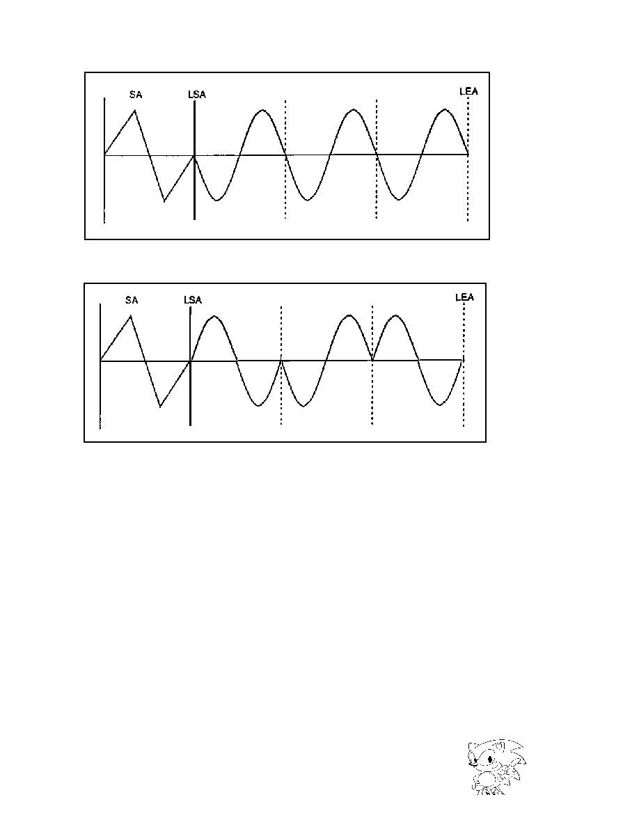
SEGA Confidential
Attack Data
Loop Data
Figure 4.26 Reverse Loop
Attack Data
Loop Data
Figure 4.27 Alternative Loop
Because the premise is that the data corresponding to "LSA" and "LEA" to be the
same in terms of normal loop and reverse loop, create the loop data by copying
"LSA" data to "LEA".
The set value of alternative loop must always be set so that "LSA"<"LEA." (If in any
of the loops "LSA">"LEA", operation can not be guaranteed.) Also, by placing data
with overlapping loop start point and loop end points the alternative pitch can be
made to match the pitch in other loop modes. When all of the wave form loop
modes are limited to the alternative loop, data corresponding to "LSA" and "LEA"
need not be the same.
52
|

SEGA Confidential
Figure 4.28 shows how the actual FM voice mixing is performed in a block diagram.
MDXSL
MDYSL
Phase Adder
Address Pointer
Wave Form
Address
Pointer
Wave Form
Data
Buffer
P G
P L F O
SOUND
STACK
DATA
SOUND
STACK
DATA
Averaging
Operation Unit
MDL
MEMORY ADDRESS
WAVE DATA
SOUND
STACK
X IN
Y IN
SOUND STACK1
SOUND STACK0
SOUND STACK2
SOUND STACK62
SOUND STACK61
SOUND STACK63
Waveform
Data
Level Multiplier
A L F O
E G
SELECTOR
2 TO 1
"O
H
"
EGDIS
SLOT OUTPUT
(TO DIGITAL MIXER)
SLOT OUTPUT
STWINH
WRITE to
SOUND STACK
Wave Form RAM
Wave Form
Phase Value
Level (Volume)
Coefficient
Figure 4.28 FM Sound Generator Configuration
Saturn SCSP User's Manual
53
|
SEGA Confidential
Each block in the FM sound generator configuration diagram is explained below.
SOUND STACK
Stores the output of each slot. The output values (sound
stack internal data) from two slots can be input into the
SCSP slot.
Averaging Operation Unit
Each slot has X and Y modulator input slots. These
values must be added together to combine them into one.
To avoid having the results of the addition go into over-
flow, the two input values are multiplied by 1/2 before
adding them together. By incorporating this method, the
SCSP can take two input values and convert them into
one output data.
By showing input data as XD and YD and the output
data as ZD, the following equation can be produced.
Z D =
X D + Y D
2
Y D
X D
Z D
Averaging Operation Unit
Figure 4.29 Averaging Operation Equation
Because this equation is the same as the equation for
obtaining the average value, this block is called the
averaging operation unit.
MDL[Modulation Level (Variation Amount)]
Used to adjust the degree of the FM effect through the
external slot input.
Phase Adder
Adds (subtracts) the phase value generated by PG (phase
generator), and the phase value generated by the MDL
calculation after passing through the averaging arith-
metic unit.
54
|

SEGA Confidential
Level Multiplier
Multiplies the wave form read from the wave form
memory, the ALFO, TL (Total Level), and the level coeffi-
cient generated by the EG. Also adjusts the actual wave
form output level.
Wave Form RAM
RAM for sound.
Wave Form Address Pointer
This block generates the actual wave form memory
address by taking the SA (start address) set for each slot
and the wave form phase value output from the phase
adder and adding or subtracting them. The loop control
and the loop status determines whether to add or sub-
tract.
Wave Form Data Buffer
Memory used for temporary storage of wave forms read
from the wave form memory.
PG (Phase Generator)
Controls the read speed of the sound frequency wave
form. (Actually, it performs skip reading.)
EG (Envelope Generator)
Generates the time-based variations of the value (enve-
lope curve) based on each rate or level setting. The value
created here is multiplied with the wave form data after
it is sent to the level multiplier. This causes timing
changes in the wave form output.
Saturn SCSP User's Manual
55
|
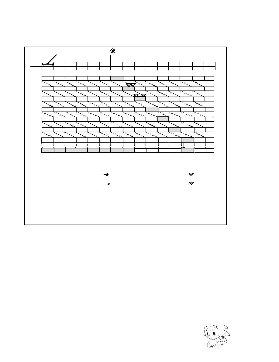
SEGA Confidential
The connections between the slots (actually, connections between the sound stack
and the slots) are important for FM voice mixing. The slot calculations in
F
igure 4.28
FM voice mixing diagram can be shown like
F
igure 4.30 below.
Figure 4.30 Slot Calculation and Sound Stack State
Slot calculation starts with the PG calculation process and the PLFO calculation
process (OP1), with the remainder executed in the following cycle: ADP (address
pointer) calculation processing and MD (modulation) data read (OP2), wave form
data read (OP3), interpolate function process and EG calculation processing and
ALFP calculation processing (OP4), level calculation processing (OP5) (OP6), wave
form output value sound stack write (OP7). The calculation process of the level
calculation takes a long time, so
two
cycles are required. If
looking
at a snapshot of
the calculation process, for example, slot 3 is doing PG calculation processing and
PLFO calculation processing while ADP calculation processing
and MD read are done
in slot 2. M
eanwhile, wave form read in slot 1, interpolate calculation process, EG
calculation process and ALFO calculation process in slot 0, level calculation process
in slot 31 and slot 30, and sound stack writing in slot 30 are also being executed.
26 27 28 29 30 31 0 1 2 3 4 5 6 7
25 26 27 28 29 30 31 0 1 2 3 4 5 6
24 25 26 27 28 29 30 31 0 1 2 3 4 5
23 24 25 26 27 28 29 30 31 0 1 2 3 4
22 23 24 25 26 27 28 29 30 31 0 1 2 3
21 22 23 24 25 26 27 28 29 30 31 0 1 2
20 21 22 23 24 25 26 27 28 29 30 31 0 1
20 21 22 23 24 25 26 27 28 29 30 31 0 1
O P 1
O P 2
O P 3
O P 4
O P 5
O P 6
O P 7
S.STK
(1/44.1K)/32=708nsec
Past Cycle
Current Cycle
Numbers in boxes indicate slot numbers.
O P 1 :OPERATION 1 : PG Calculation Process, PLFO Calculation Process
O P 2 :OPERATION 2 : ADP (Address Panter) Calculation Process
MD (Modulation Data) Read (From the Sound Stack)
Executing in timing shown by in drawing
O P 3 :OPERATION 3 : Read Wave Form Data (FROM DRAM)
Executing in timing shown by in drawing
O P 4 :OPERATION 4 : Interpolate Calculation Process, EG
Calculation Processing ALFO Calculation Process
O P 5 :OPERATION 5 : Level Calculation Process
O P 6 :OPERATION 6 : Level Calculation Process
O P 7 :OPERATION 7 : Writes the Wave Form Output Value to the Sound
Stack.
Executes in the timing shown by the -->and in
the drawing.
56
Address pointer
|
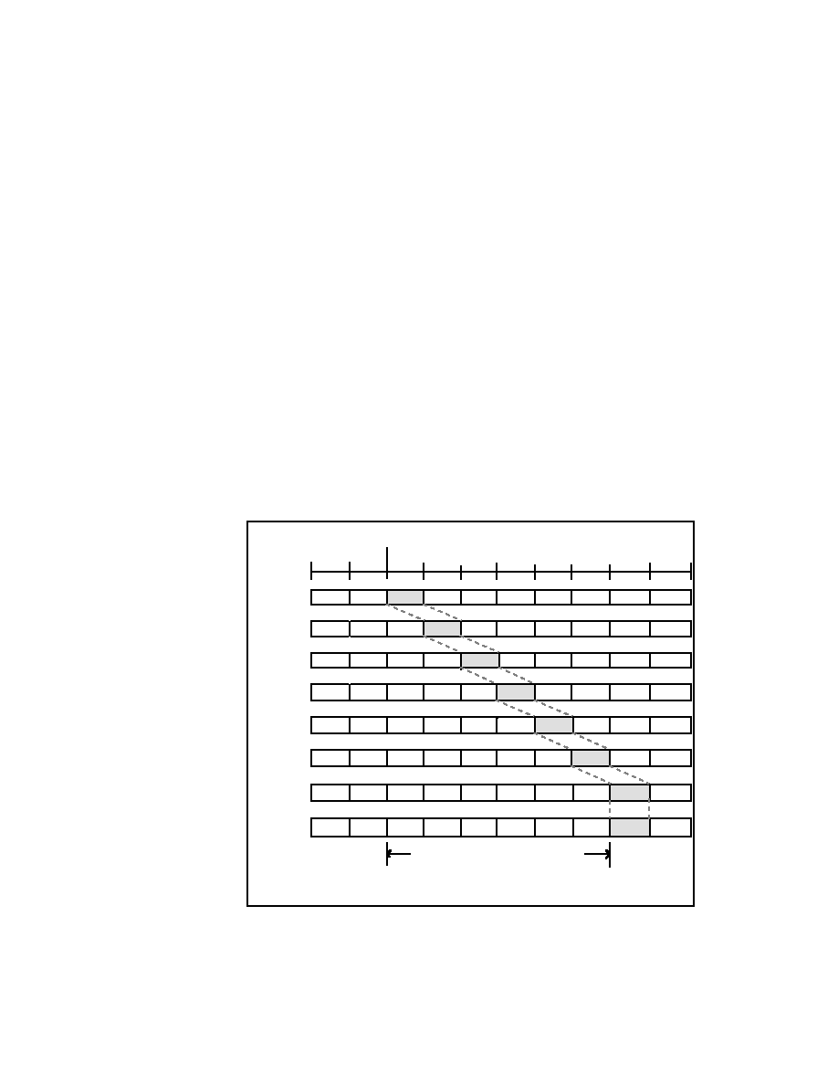
SEGA Confidential
Because slot calculation starts at slot 0 and moves towards slot 31, the data written to
the sound stacks also start at a low number and move up. However, there is a time
difference between the time the slot calculation starts and the time the slot is written
to the sound stack, which is equal to the calculation execution time. For example
Figure 4.31 shows that it would take six cycles worth of time for slot 0 to be written
to the sound stack.
As shown in Figure 4.30, when connecting a slot to another slot, the slot being con-
nected to must already have written its data to the sound stack when it is in the OP2
state or the connection cannot be done.
For example, since up to 27 slots are written to the sound stack, up to "27" color-
coded sound data sets are applicable to slots that can be connected to slot 0 when
OP2 is slot 0. An equation expressing this would be as follows.
{Current slot number + 32
number of the slot to be connected (sound stack) + A}
5
The current slot number represents the register slot number. However, if the sound
stack of the slot to connect is in the current slot, then A is "32"; for past cycles, enter
"0". Here the past cycle indicates the cycle data from one sample previous.
30
31
0
1
2
3
4
5
6
7
29
30
31
0
1
2
3
4
5
6
28
29
30
31
0
1
2
3
4
5
27
28
29
30
31
0
1
2
3
4
26
27
28
29
30
31
0
1
2
3
25
26
27
28
29
30
31
0
1
2
24
25
26
27
28
29
30
31
0
1
1
0
24
25
26
27
28
29
30
31
op1
op2
op3
op4
op5
op6
op7
S.STK
S.STK: Sound Stack
6 Cycles Worth of
Time Until SLOT0 is
Written to the Sound
Stack
Past
Cycle
Current
Cycle
Figure 4.31 Time Lag until the Slot Is Written to the Sound Stack
Saturn SCSP User's Manual
57
|
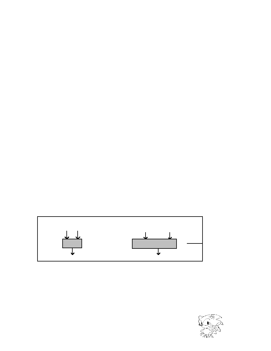
SEGA Confidential
At least two slots must be connected to enable voice mixing. Explained below is the
calculation method used for "MDXSL" and "MDYSL" (each 6 bits).
When two slots are connected, the slot applying modulation (Modulator) is M, while
the slot being modulated (carrier) is called C. The results of MC are called J, with
the resulting equation shown below.
M C = J . . . . equation 4.1
The resulting J value changes the "MDYSL" and MDSYL" highest bit (6th in MSB)
value. The conditions for this are shown below.
· Condition 1 J
28
- Convert the J value into hexadecimal 5 bit value.
- If it is the newest sample then MSB (6th bit) is "0B"; if past
samples, it is "1B".
· Condition 2 J < 0 (J is negative)
- Calculate 32 + J (calculate 10 decimal)
- Next convert the value from (1) to a hexadecimal 5 bit value.
- If it is the newest sample then MSB (6th bit) is "0B", if past
samples, then it is "1B".
· Condition 3 When the value J does not fit in neither condition 1 nor 2 above.
- Convert the J value into hexadecimal 5 bit value.
- If it is the newest sample then MSB (6th bit) is "1B", if past
samples, then it is "0B".
Following are items to be aware of when using FM voice mixing.
X Y
X
Y
X+Y
2
Slot Input Output
Modulator Input
To ADDRESS POINTER
Averaging
Operation Block
Waveform Data Output
SLOT
··· Modulator Input
=
Figure 4.32 Slot Averaging Calculation
58
|
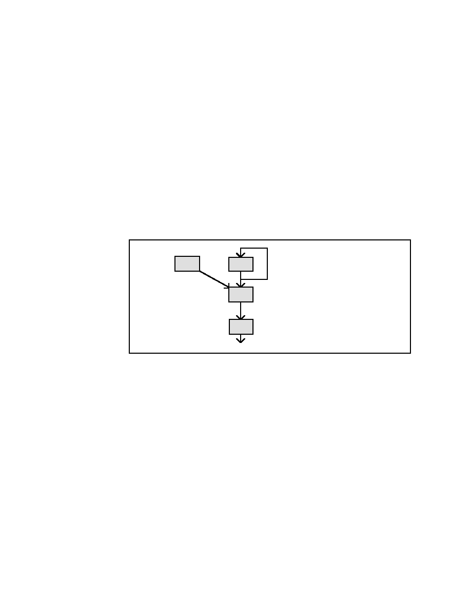
SEGA Confidential
The source input into a slot is the data in the sound stack ("SOUS"). Therefore,
modulating with a slot indicates that the sound stack corresponding to the modula-
tion slot is assigned and connected to a non-modulation slot. Actual functions
include selecting the sound stacks input for modulator input Y and X, using
"MDXSL" and "MDYXL"; therefore, the parameters obtained using the calculation
method explained at the beginning of this register is required.
Also, there are two modulator inputs to the slot, X and Y. Be aware that these may
be cut in half through the averaging calculation. Therefore, if only one slot is being
connected to the slot, X and Y are set with the same parameters and the same slot
sound stack data should be input. If only one side is set for input, then unexpected
data may get in and make the FM modulation rate could seem smaller, or other such
effects.
Next, determine each parameter using the "MDXSL" and "MDYSL" calculation
method withfour slot configurations using the actual FM voice mixer as an example.
First, explain how to get the FM voice mixer algorithm as shown in Figure 4.33.
S1 S0 Sn: Shows Slot n
S2
Arrow shows
data flow.
Algorithm sample
(Y M 2 1 5 1 : FM CONNECTION)
S3
Figure 4.33 4SLOT configuration Algorithm
· Slot0
Slot0 output is used as input for slot 2, but the output of slot0 is used for the
input of slot0. This is called self feedback.
· Slot1
Slot1 output is used as input for slot2.
· Slot2
Slot2 uses the output of slot1 and slot0 as its input. This output is used as input
for slot3.
Saturn SCSP User's Manual
59
|
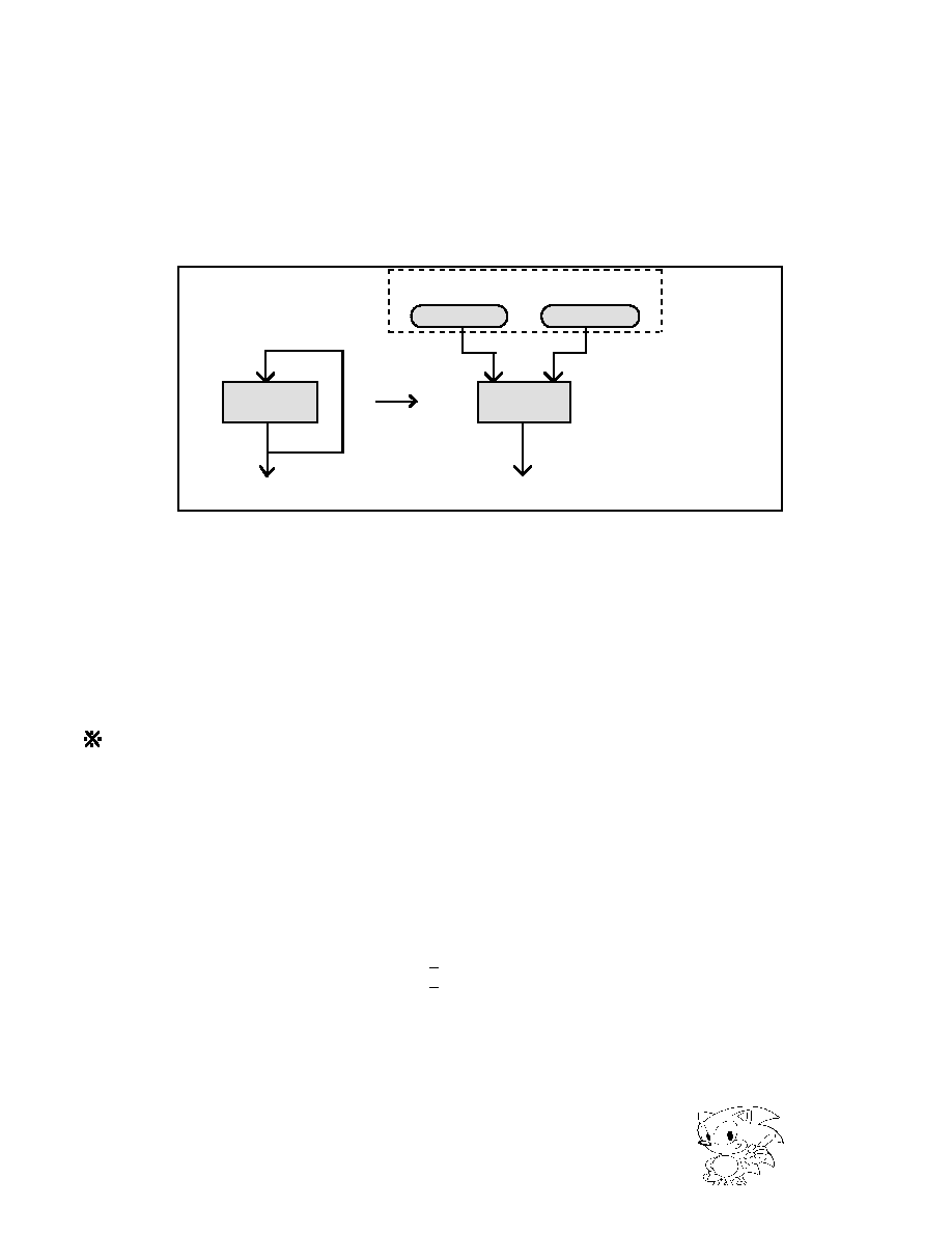
SEGA Confidential
· Slot3
Slot3 uses slot2 output as input. Slot3 output is not connected to anything, but is
used as voice output.
(1) Parameters set in SLOT0.
[FM Algorithm]
[Actual diagram]
SOUND STACK
Y
X
SLOT0
SLOT0
SLOT0
SLOT0
Figure 4.34 SLOT0 Algorithm
For a self feedback type configuration such as slot 0, connect the sound stack that
stores the slot 0 output data to the modulation input X and Y.
There are three different ways of input methods to input the latest and past sample
to both modulation input X and Y, or latest sample to one side and past sample to
another since there are latest and past sample currently calculated in sound stack.
Caution
:
In the case of self feedback, oscillation may occur as the same sample is input. So
please input latest samples to one side and past samples to the other.
The values of <MDXSL and MDYSL are both 0 for the modulator slot and the
modulated slot, so entering these values into equation 4.1 produces the following
results.
0 0 = 0
This meets the requirements of condition 3 in equation 4.1, so MSB of MDXSL and
MDYSL are as follows.
Latest samples
MSB=1 (100000)B = 20H
Past samples
MSB=0 (000000)B = 00H
60
|
SEGA Confidential
(2) Parameters set in SLOT2
SOUND STACK
SLOT2 SLOT2
SLOT1 SLOT0
X(Y)
Y(X)
SLOT1
SLOT0
[FM Algorithm]
[Actual diagram]
Figure 4.35 SLOT2 Algorithm
Because slot 2 is input for multiple slots, there is no need to worry about whether to
use latest or past samples.
The "MDXSL" and "MDYSL" values input (slot 1 side) into slot 1 are "1" for the
modulator slot and "2" for the modulated slot. Applying this to equation 4.1 results
in the following.
1 2 = 1
This meets the requirements of condition 2 in equation 4.1, so the MSB of "MDXSL"
and "MDYSL" are as follows.
32 + (1) = 31 = 1FH = (011111)B
Latest samples
MSB=0 (011111)B = 1FH
Past samples
MSB=1 (111111)B = 3FH
SLOT1
SLOT0
SLOT2
SLOT2
SLOT1 Side
SLOT0 Side
Figure 4.36 SLOT2 Algorithm (By input slot)
Saturn SCSP User's Manual
61
|

SEGA Confidential
The "MDXSL" and "MDYSL" values input (slot 0 side) into slot 0 are "0" for the
modulator slot and "2" for the modulated slot. Applying this to equation 4.1 results
in the following.
0 2 = 2
This meets the requirements of condition 2 in equation 4.1, so the MSB of "MDXSL"
and "MDYSL" are as follows.
32 + (2) = 30 = 1EH = (011111)B
Latest samples
MSB=0 (011110)B = 1EH
Past samples
MSB=1 (111110)B = 3EH
Note:
As a rule, always input the same generation sample when inputting slots with different
numbers. Past FM sound generators have used this method, so when replacing an FM
sound generator tone library, use this method.
(3) Parameters Set in Slot 3
SOUND STACK
SLOT2
SLOT3
SLOT3
SLOT2
[FM Algorithm]
[Actual diagram]
Figure 4.37 SLOT3 Algorithm
Because there is only one input for slot 3, input the output of slot 2 for the modula-
tor input of both X and Y.
If the connected slots are different, there is no chance of oscillation, so both modula-
tor input X and Y can have just the latest sample, or just the past samples, or the
latest in one side and past in the other side. If replacing an existing FM sound gen-
erator tone library, use one sample or the other.
62
|

SEGA Confidential
The "MDXSL" and "MDYSL" values input into slot 2 are "2" for the modulator slot
and "3" for the modulated slot. Applying this to equation 4.1 results in the follow-
ing.
2 3 = 1
This meets the requirements of condition 2 in equation 4.1, so the MSB of "MDXSL"
and "MDYSL" are as follows.
32 + (1) = 31 = 1FH = (011111)B
Latest samples
MSB=0 (011111)B = 1FH
Past samples
MSB=1 (111111)B = 3FH
Saturn SCSP User's Manual
63
|

SEGA Confidential
Up until now, "MDXSL" and "MDYSL" values have been achieved through calcula-
tion. However, by using the parameter table shown in Table 4.16, and from the
modulator and carrier slot numbers, we can get the output of the "MDXSL" and
"MDYSL" values.
Below, using the parameter table, the values for "MDXSL" and "MDYSL" can be
found in Figure 4.33.
(1)
Parameters set in slot0
Slot 0 is a self-feedback configuration so the carrier slot number and the
modulator slot number are "00". From this, "MDXSL" and "MDYSL" values
from the parameter table are as follows.
Latest samples
20H
Past samples
00
H
As explained earlier, if the same generation samples are used in the self-
feedback configuration, there is a chance for oscillation, so avoid this method.
(2)
Parameters set in slot2
Slot 2 uses the multiple input configuration.
First, when slot 1 is input, the carrier slot number is "02" and the modulator
slot number is "01". The MDXSL" and "MDYSL" values from the parameter
table are as follows.
Latest samples
1FH
Past samples
3F
H
Next, when slot 0 is an input, the carrier slot number is "02" and the modulator
slot number becomes "00". The MDXSL" and "MDYSL" values from the
parameter table are as follows.
Latest samples
1EH
Past samples
3E
H
(3)
Parameters set in slot3
Slot 3 uses the output of slot 2, thus the carrier slot number is "03" and the
modulator slot number is "02". The "MDXSL" and "MDYSL" values from the
parameter table are as follows.
Latest samples
1F
H
Past samples
3FH
64
|
SEGA Confidential
Table 4.16 Relation of MDXSL/MDYSL and SLOT
How to use the table
First find the carrier side slot number and then find the modulator slot number
which is input into the carrier side. Find the number of sample that corresponds
in the horizontal column.
Saturn SCSP User's Manual
65
|
SEGA Confidential
Next, the "MDL" (Modulation Level) will be explained. "MDL" is the modulation
rate (how much modulation) parameter used to set the modulation signal added to
the modulation input X and Y. If this value becomes large, the frequency modula-
tion will be quite deep; if the value becomes small, the level will be more shallow.
(Figure 4.38)
MDL Large
MDL Small
Intersection
The only thing
that changes in
the MDL variations
is the amplitude.
(The intersection
does not change.)
Figure 4.38 MDL Modulation Rate
Here the modulation rate of the "MDL" set value is explained. Table 4.15 shows the
modulation rate becomes
±
n
by the "MDL" setting.
Each sound slot data item input into the modulation input X and Y is averaged in
the averaging calculation block. Data input into X is XD, into Y is YD, and let the
output to averaging calculation block be ZD, then the following equation can be
represented.
ZD = ( XD + YD ) / 2
This "ZD" is adjusted by the "MDL" and sent to the slot address pointer (phase
adder).
66
|
SEGA Confidential
Read
wave
form
address
Phase
No modulation input
At positive
maximum
shift
Time
Phase
With modulation input
(sine wave input)
At negative
maximum
shift
Time
Figure 4.39 Maximum Shift of the Wave Form Read Address
When modulation wave form is not added to FM voice mixing, the time phase
function is linear. However, if the modulation waveform is added, because a phase
shift equivalent to the modulation waveform will be added, the linear time-phase
waveform will then become non-linear. This shift becomes maximum when ZD
assumes the
±
maximum value. MDL modulation rate indicates the wave form
address shift (maximum shift) when the wave form data (sine wave) is at 1 cycle =
1Kword and ZD is
±
the maximum value.
Table 4.17 Address Maximum Shift Value According to the Register Setting Value
Compare Table 4.16 and Table 4.17 to get the function
= 512 (when MDL=AH). In
Table 4.16, there is wave form data (sine wave) consideration where 1 cycle = 1K
word (1024 words), but mathematically 1 wave form cycle length is defined as 2
.
Therefore, in the current FM voice mixer the sine wave used is 1 cycle = 1 Kword so
the maximum shift of 512 can be expressed as
. Using
to express the shift is only
valid when 1 cycle of wave form data is 1 K word. Otherwise, use the expression
method by address shift shown in Table 4.17.
When using the FM voice mixer, always have three cycles of wave form data. The
reason has to do with address shift. The SCSP hardware must hold up to 1Kword
address shift (MDL="AH"), but if the amount exceeds 1Kword, the hardware will
automatically execute clipping processing, so there is no need to have extra wave
form data equal or greater than 1Kword.
MDL [3:0]
0 ~ 4
5
6
7
8
9
A
B
C
D
E
F
Address max.
shift
±
0
32
64
128
256
512
1024 2048
4096
8192
16384
32768
Saturn SCSP User's Manual
67
|
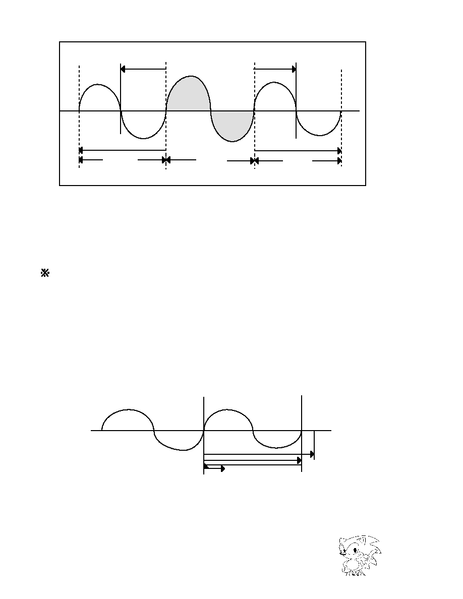
SEGA Confidential
1 K
1 K
1 K
-2
shift
range
-
shift range
However, be aware that 1 K=2 =1024.
10
+
shift range
SA/LSA
LEA
+2
shift range
Figure 4.40 Address Shift during FM Voice Synthesis
During FM voice mixing,
place only the additional amount required for address
shift. As a rule, operation will run without problems if
worth of wave form data is
set before "SA", and after "LEA" and is
±
. However, using three cycles worth of
data as shown in Figure 4.40 is the ideal setting method.
Concerning Clipping Process
This relates to the address shift described earlier. The address shift range shifts a
maximum of
±
32768 addresses, so before and after the basic wave form respec-
tively 32 cycles (32Kwords) and 16 cycles (16Kword) worth of wave form data is
required for total memory requirements of 65Kwords.
For this reason, the SCSP clips (process to prevent shift from exceeding a limit) shift
that exceeds 1K word and returns the shift to 0. So if there is 3K word worth of
wave form data no matter how much shift there is, it is more than enough to cover
requirements. Clipping process was done because the valid address bits available
for shift was 10.
Phase
Auxiliary wave form
0
2
Figure 4.41 Wave Data During Clipping Process
As shown in Figure 4.41, even if the wave form exceeds the auxiliary waveform after
the shift, it returns to 0 at the point where phase exceeds 2
.
68
|
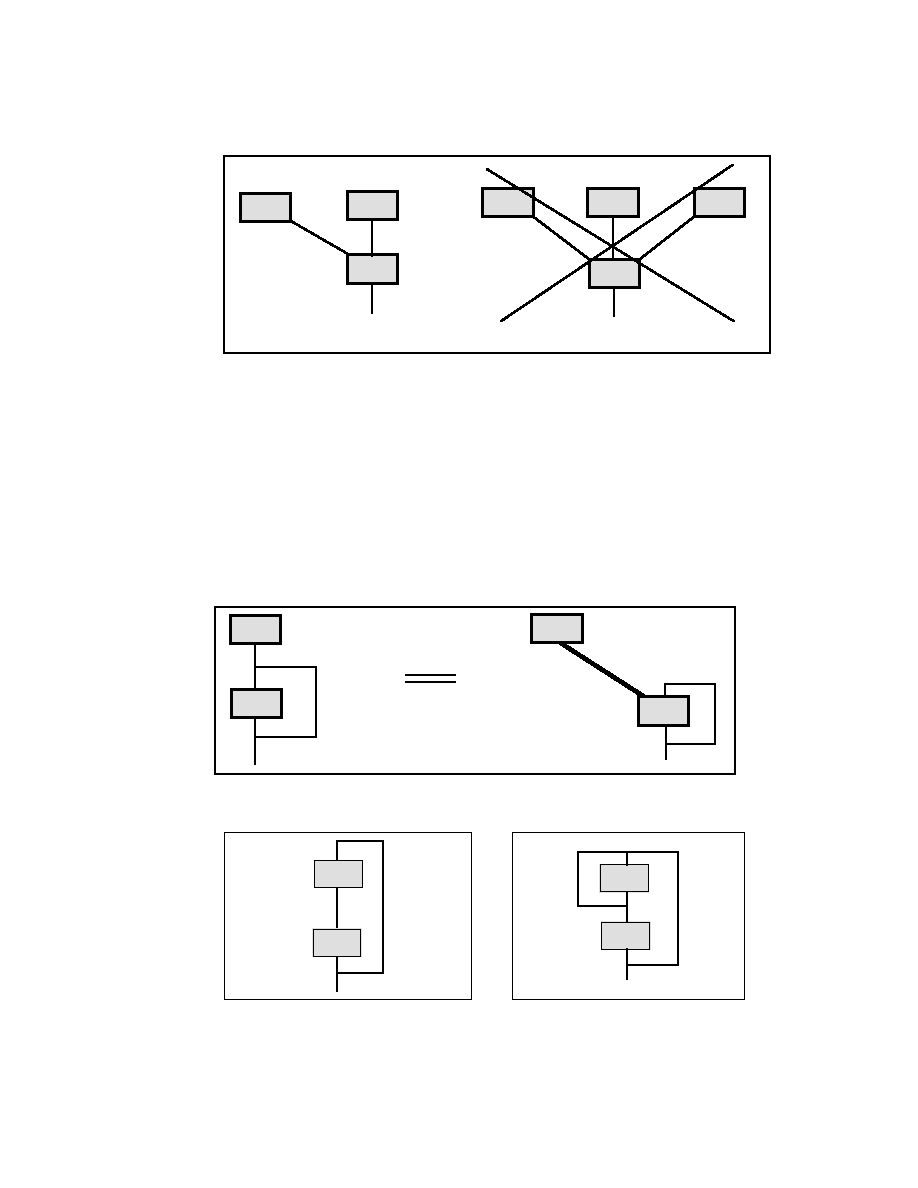
SEGA Confidential
The following is an explanation of the SCSP FM configuration (algorithm). The
SCSP slot is configured with two inputs and one output so the number of slots that
can be connected (modulation can be applied) to one slot is a maximum of two.
SLOT
SLOT
SLOT
SLOT
SLOT
SLOT
SLOT
This is possible
This is not possible
Figure 4.42 Slot Connection Count
As shown in Figure 4.42, modulation is possible if it's up to two modulators. Also if
the modulation data (source) is brought up from the sound stack, FM configurations
shown in Figure 4.43, Figure 4.44, Figure 4.45, and Figure 4.46 are possible.
(Figure 4.43 is a self-feedback slot with still another slot modulating the first slot;
Figure 4.44 combines multi-stage slots for a multi-stage feedback; Figure 4.45 com-
bines the multi-stage feed back and self feedback for a composite-type feedback;
Figure 4.46 shows a composite modulation type slot modulated by a multi-stage
feed back and further modulated by another slot.)
SLOT
SLOT
SLOT
SLOT
The algorithm for both
left and right diagrams
is the same
Figure 4.43 Self-Feedback Modulation
SLOT
SLOT
SLOT
SLOT
Figure 4.44 Multi-Stage Feedback Figure 4.45 Composite Feedback
Saturn SCSP User's Manual
69
|
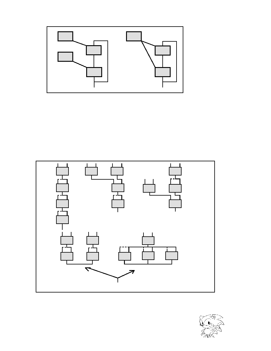
SEGA Confidential
SLOT
SLOT
SLOT
SLOT
SLOT
SLOT
SLOT
Figure 4.46 Composite Modulation
Figure 4.47 and 4.48 show specific examples of a basic FM configuration which
should be used as a reference for FM voice mixing. Each slot upper side has two
modulation inputs while the line on the lower side shows the slot output.
In addition, make sure that the dotted lines are also connected (refer to the
forementioned figures.
SLOT
SLOT
SLOT
SLOT
SLOT
SLOT
SLOT
SLOT
SLOT
SLOT
SLOT
SLOT
SLOT
SLOT
SLOT
SLOT
SLOT
SLOT
SLOT
SLOT
This is acomplished by mixing the lower stage slot output.
Figure 4.47 FM Configuration Algorithm Pattern 1
70
|
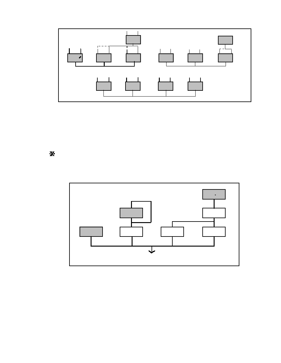
SEGA Confidential
SLOT
SLOT
SLOT
SLOT
SLOT
SLOT
SLOT
SLOT
SLOT
SLOT
SLOT
SLOT
Figure 4.48 FM Configuration Algorithm Pattern 2
If the uppermost slot in FM voice mixing does not have self-feedback, there is noth-
ing to be connected. In this situation, set "0~4" values to "MDL" value and the
modulation rate to "0". This is how modulation input is set to "0".
Definition of the uppermost slot.
The uppermost slot is the highest slot in each of the algorithm towers. In Figure
4.49, there are three towers: the S0 tower, the S1, S2 tower, and the S3, S4, S5, S6
tower. The uppermost slots are S0, S1, and S6.
1 SOUND OUTPUT
SO
S1
S2
S3
S4
S6
S5
Figure 4.49 7 SLOT FM Configuration
Saturn SCSP User's Manual
71
|
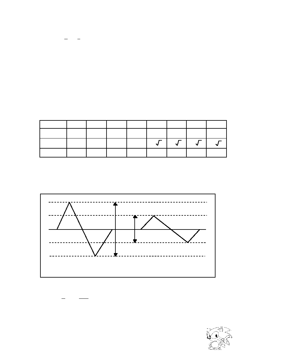
SEGA Confidential
Volume Register
TL[7:0] (R/W) ;Total Level
The total value of attenuation volume of the area where
bit is set to "1", which is within total level 8 bit, becomes
the actual attenuation volume [dB]. Therefore, the larger
the value set in "TL", the larger the attenuation volume,
making the sound volume less. On the other hand, the
smaller the value set in "TL," the smaller the attenuation
level, and the greater the sound volume will be .
For example, "the attenuation volume with "FF
H
" would
be as shown below.
- 48 - 24 - 12 - 6 - 3 - 1.5 - 0.8 - 0.4 = -95.7[dB]
Table 4.18 TL, Attenuation, and Waveform Amplitude
If only bit 4 is set to "1", then the amplitude of the output
wave form after the TL calculation will be 1/2 of the
amplitude of the wave form in memory, as shown in
Figure 4.50.
Data in the wave
form memory
Amplitude after TL
operation
1
1/2
Figure 4.50 Wave Data when TL bit 4 = 1
SDIR (R/W) ; Sound DIRect
This flag is used to determine whether or not to directly
output the sound data. When this bit is "1," then sound
data is output without being multiplied by EG, TL,
ALFO, etc., calculations.
72
TL bit
bit 7
bit 6
bit 5
bit 4
bit 3
bit 2
bit 1
bit 0
TL
Attenuation
- 48
- 24
- 12
- 6
- 3
- 1.5
- 0.8
- 0.4
Amplitude
Ratio
1/256
1/16
1/4
1/2
1/
1/
1/
1/
Real Number
Ratio (times)
0.00391
0.06250
0.25000
0.50000
0.70711
0.84090
0.91700
0.95760
2
2
4
2
8
2
16
|
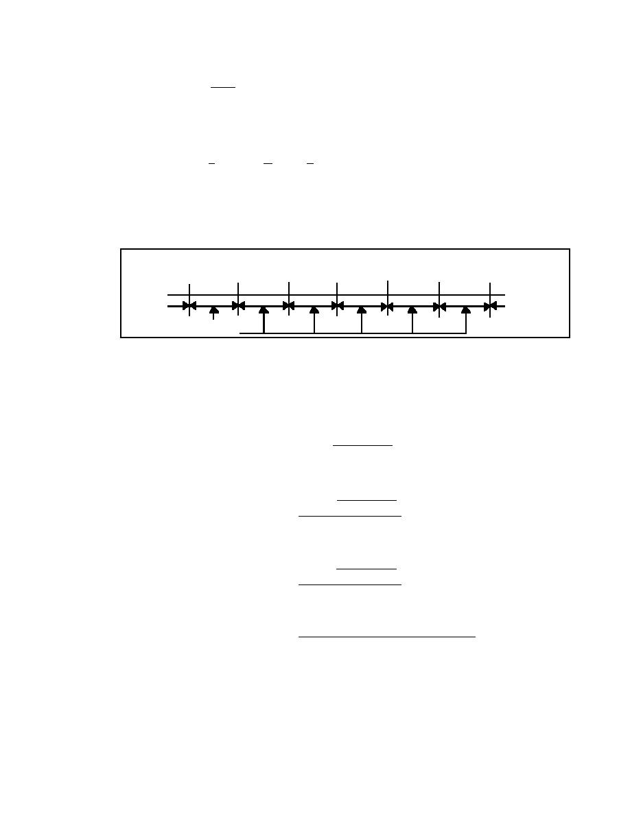
SEGA Confidential
PITCH Register
OCT[3:0] (R/W) ; OCTave
The function of the "OCT" register is to increase or de-
crease the sound generation frequency by octave with
respect to the wave form data stored in memory.
FNS[9:0] (R/W) ; Frequency Number Switch
The function of this register is to adjust the tone between
the octaves raised or lowered with "OCT." When the
"FNS" and "OCT" values are both "0," the tone matches
the sampling source data. Figure 4.51 shows the relation
of the "FNS" and "OCT" values.
... OCT="D
H
" OCT="E
H
" OCT="F
H
" OCT="O
H
" OCT="1
H
" OCT="2
H
" OCT="3
H
" ...
... FNS="0
H
" FNS="0
H
" FNS="0
H
" FNS="0
H
" FNS="0
H
" FNS="0
H
" FNS="0
H
" ...
F/8 F/4 F/2 1F 2F 4F 8F
FNS set range
Frequency
Figure 4.51 Relation of OCT and FNS
The actual pitch (n) is calculated by the equations shown
below.
n(Cent)
=
1200
×
LOG
2
1024
+
FNS
1024
=
1200
×
LOG
10
1024
+
FNS
1024
LOG
10
2
=
1200
×
LOG
10
1024
+
FNS
1024
0.30103
=
1200
×
LOG
10
(1024
+
FNS)
-
10
×
0.30103
0.30103
The value found with this equation is expressed in units
of "Cents."
Saturn SCSP User's Manual
73
|
SEGA Confidential
One "cent" is 21/1200=1.000577789 times. Also, one
octave is 1200 cents. When cent = n, then 2n/1200 times
{=(1.000577789)n} against the original frequency. There-
fore, the equation below is used to find the n cent high
tone frequency Fn [Hz] in relation to the basic frequency
tone Fo [Hz].
Fn [Hz] = Fo x 2n/1200
Table 4.19 shows the actual frequencies corresponding to
the cent count (number of cents).
Table 4.19 Actual Frequency Corresponding to Cent Count
Next, using the sound of C4 (do) sampled at a rate of
44.1KHz as an example, the method for setting "FNS" and
"OCT" will be explained.
FNS = 2
10
x (2
P/1200_
1)
By setting each parameter as shown in Table 4.20 from this
equation, you can output at any frequency.
Cent Count
Actual Frequency Value (XFo)
0
1.000000000
100
1.059463094
200
1.122462048
300
1.189207115
400
1.259921050
500
1.334839854
600
1.414213562
700
1.498307077
800
1.587401052
900
1.681792830
1000
1.781797436
1100
1.887748625
1200
2.000000000
74
|
SEGA Confidential
Table 4.20 FNS.OCT Parameter Table
Note Name
Note No.
PITCH
[Cent]
FNS [9:0]
[DEC]
FNS [9:0]
[HEX]
OCT [3:0]
[HEX]
B3
59
1100
909.1
38D
F
C4
60
0
0.0
0
0
C4#
61
100
60.9
03D
0
D4
61
200
125.4
07D
0
D4#
63
300
193.7
0C2
0
E4
64
400
266.2
10A
0
F4
65
500
342.9
157
0
F4#
66
600
424.2
1A8
0
G4
67
700
510.3
1FE
0
G4#
68
800
601.5
25A
0
A4
69
900
698.2
2BA
0
A4#
70
1000
800.6
321
0
B4
71
1100
909.1
38D
0
C5
72
0
0.0
0
1
Saturn SCSP User's Manual
75
|
SEGA Confidential
LFO Register
LFO is a low-frequency oscillator that is used for modulation of sound signals
The LFO is contained in each slot and has the amplitude modulation output and
frequency modulation output for that slot.
There are four types of output wave form from the LFO. These are: sawtooth wave,
rectangular wave, triangle wave, and noise (white noise). All of these can be selected
freely.
The LFO block diagram is shown in Figure 4.52. All waves (except the noise) can be
reset and the frequency changed. Excluding the noise waveform, resetting as well as
changing the frequency of sawtooth waveform, rectangular waveform, and triangu-
lar waveform are allowed. Also, the modulation rate and the LFO wave form can be
set independently for both the amplitude modulation and the frequency modulation
side.
LFO wave form oscillator
Sawtooth
wave
Rectangular
wave
Triangular
wave
White noise
LFORE LFOF
SELECTOR
4
TO
1
ALFOS
To Amplitude
Modulation
Amplitude Modulation
Rate Adjustment
PLFOWS
ALFOWS
PLFOS
SELECTOR
4
TO
1
To Frequency
Modulation
The MSB side is reversed so the
ALFO wave form and the
PLO wave form are different.
Frequency Modulation
Rate Adjustment
Figure 4.52 LFO Block Diagram
76
|
SEGA Confidential
LFORE (R/W) ;LFO REset
Sets the LFO reset to yes or no. If this bit is set to "1", the
LFO is reset. If "0" is written then operation starts.
LFOF [4:0] (R/W) ;LFO Frequency
Designates the LFO oscillation frequency.
Table 4.21 Oscillation Frequency of the Oscillator
ALFOS[2:0] (R/W) ;Amplitude-LFO Sensitivity
Sets the degree of amplitude modulation through the
LFO. The tremor effect (a phenomenon that occurs when
the sound volume is changed in a cyclic pattern) can be
expressed through this amplitude modulation.
LFOF
Oscillation Frequency (Hz)
LFOF
Oscillation Frequency (Hz)
00
H
0.17
10
H
2.87
01
H
0.19
11
H
3.31
02
H
0.23
12
H
3.92
03
H
0.27
13
H
4.79
04
H
0.34
14
H
6.15
05
H
0.39
15
H
7.18
06
H
0.45
16
H
8.6
07
H
0.55
17
H
10.8
08
H
0.68
18
H
14.4
09
H
0.78
19
H
17.2
0A
H
0.92
1A
H
21.5
0B
H
1.10
1B
H
28.7
0C
H
1.39
1C
H
43.1
0D
H
1.60
1D
H
57.4
0E
H
1.87
1E
H
86.1
0F
H
2.27
1F
H
172.3
Saturn SCSP User's Manual
77
|
SEGA Confidential
ALFOWS[1:0] (R/W) ; Amplitude-LFO Wave Select
Designates AM modulation wave form as shown in Table
4.22.
Table 4.22 LFO AM Modulation Wave Form by LFO
PLFOWS[1:0] (R/W) ; Pitch-LFO Wave Select
Designates PM modulation wave form as shown in Table
4.23.
Table 4.23 LFO PM Modulation Wave Form
ALFO[7:0] and PLFO[7:0] show the LFO output bit width
(data).
ALFOWS
AM Modulation (ALFO)
Volume
ALFO[7:0]
0
-0 dB
0
FF
1
-0 dB
0
FF
2
-0 dB
0
FF
3
-0 dB
0
FF
*******************************
*******************************
************Noise*************
*******************************
*******************************
PLFOWS
AM Modulation (PLFO)
Pitch
PLFO[7:0]
0
+
0
7F
00
80
1
+
0
7F
00
80
2
+
0
7F
00
80
3
+
0
7F
00
80
*******************************
*******************************
************Noise*************
*******************************
*******************************
78
|
SEGA Confidential
PLFOS[2:0] (R/W) ; Pitch-LFO Sensitivity
Specifies the degree of frequency modulation through the
LFO. The vibrato effect (a phenomenon that occurs when
the sound frequency is changed in a cyclic pattern) can be
expressed through this frequency modulation (Table
4.24).
Table 4.24 Rates of Amplitude and Frequency Modulation
ALFOS
Mixing to the EG
PLFOS
Effect on Pitch
0
1
2
3
4
5
6
7
No effect
Displacement of 0.4 dB
Displacement of 0.8 dB
Displacement of 1.5 dB
Displacement of 3 dB
Displacement of 6 dB
Displacement of 12 dB
Displacement of 24 dB
0
1
2
3
4
5
6
7
No effect
Displacement of
±
7 cent
Displacement of
±
13.5 cent
Displacement of
±
27 cent
Displacement of
±
55 cent
Displacement of
±
112 cent
Displacement of
±
230 cent
Displacement of
±
494 cent
Saturn SCSP User's Manual
79
|

SEGA Confidential
MIXER Register
The digital mixer block in the SCSP is used to adjust the level and balance of the
various sound signals. It is made up of the direct mixer adjustment block, the DSP
input (stage adjust) mixer block, the DSP output (stage adjust) mixer block and the
last output (stage adjustment) mixer block. Figure 4.53 shows the digital mixer
block diagram.
DIRECT
IN
MIXER
OUT
MIXER
LAST
MIXER
DSP
Figure 4.53 Digital mixer block diagram.
Direct Sound Adjustment Block
This mixer block controls the circuit that connects the output of each slot directly to
the DAC output. It can control the output level ("DISDL") and output balance
("DIPAN") for each slot.
DSP Input Step Adjustment Block
Conducts mixings required to input the output of each slot to the DSP ("MIXS"). In
reality, in the "ISEL" of each slot, the "MIXS" that inputs audio signal is selected and
the input level is adjusted by the "IMXL". When mixing multiple sounds with the
"ISEL", each of the sounds must be balanced.
Because the "MIXS" can mix the output from multiple slots and then input the
result, the same effect like BGM reverb can be applied to many sounds. If effects at
the DSP are applied, the sound data is sent to "MIXS".
DSP Output Step Adjustment Block
The sounds that have had effects applied in the DSP or sounds that were brought in
from an external digital input pass through mixing processing and are eventually
compiled in stereo. The output level ("EFSDL") and output balance ("EFPAN") can
be adjusted for sound signals that are output from the "EFREG" that correspond to
DSP, and "EXTS" that receive external digital audio input. The data compiled here
is mixed with the direct sound mixer.
80
|

SEGA Confidential
Final Step Output Adjustment Block
Combines the direct component and the effect component of the sound and adjusts
the output level to the DAC. The final output level is adjusted by "MVOL".
About the direct component and the effect component
When effects are applied to sound, the sound without effects applied (dry) and
sounds with effects applied (wet) are mixed with the appropriate balance for
each of the screens. The internal effect program separates the dry and wet data
in the DSP. Because the sounds are mixed together in the end, when creating
dry and wet data in the DSP, there is no need to output the direct component.
This is accomplished by setting DISDL to "0" for no output. Figure 4.54 shows
the circuits of the direct component and the effect component.
DSP
MIXING
EFFECT
DSP Circuit
From Slot
DIRECT
Component
DIRECT
Processing
Output
MIXING
Processing
EFFECT
Processing
DIRECT (DRY)
+
EFFECT (WET)
When creating both direct and
effect components on the DSP
side, use the "DISDL" = "0" to cut
the direct component circuit.
Figure 4.54 Direct and Effect Component Circuits
When rewriting the DSP program, the DSP operation becomes unstable and
the sound will not be output properly from "EFREG". Set "EFSDL" to "0
H
"
to prevent sound from being output.
Saturn SCSP User's Manual
81
|
SEGA Confidential
About fixed position
The SCSP digital mixer supports 31 levels of panning, but to set it in even more
detail, use the DSP built into SCSP, as shown in Figure 4.55, to perform
(process) panning.
Source Data
EFPAN X
EFSDL X
Source Data
ESREG Y
ESREG X
Source Data
Coefficient Data
Fixed position
calculator
Send level
calculator
X
Multiply
Coefficient Data
X
Multiply
From Slot, etc.
EFPAN Y
EFSDL Y
Fixed position
calculator
Send level
calculator
X, Y values
are arbitrary
DSP Block
Coefficient Data/ RAM
Coefficient Data/ RAM
Settings are optional, but it is
best to have both channels the same.
Setting is arbitrary
Setting 1FH
Setting 0FH
Left channel output
Right channel output
Figure 4.55 DSP Panning Calculation
Figure 4.56 shows a digital mixer block diagram.
82
|
SEGA Confidential
Cumulative Adder Block
Effect DSP
Saturn SCSP User's Manual
83
|
SEGA Confidential
Next, the method for setting each of the parameters based on Figure 4.56 will be
explained.
The settings of "IMXL", "ISEL", "DISDL", and "EPSDL" are required as described
below to prevent overflow when many sounds are produced, and to prevent the
overall volume from being too low when only a few sounds are produced.
(a)
DSP Input Side Mixer
The parameters that are equivalent to the DSP input side mixer are the "IMXL"
and "ISEL" parameters.
"MIXS" (the mix stack will be explained later) can input the output of multiple
slots. This register has the ability to mix multiple data. Here the "IMXL" value
must be set at the correct level to prevent "MIXS" from overflowing.
The number of available input sounds when the "IMXL" value is changed is
shown in Table 4.25. For example, if "IMXL" is set to 7H against the input
source and the input level of "MIXS" to "0[dB]", then the number of available
input slots would be one sound worth.
Table 4.25 Relation of the source count that can input into "IMXL" and "MIXS"
(b)
"DISDL" and "EFSDL"
"DISDL" and "EFSDL" have basically the same philosophy as "IMXL," but
they must determine the sound output total count.
The sound output total count is the total sound output including the direct,
effect and external input components. This indicates the cumulative total
sources of L/R in Figure 4.56 that is being output. (L/R are counted as 1
together.) From this it is clear that the sum total of slots outputting sound is
not equal.
"IMXL" Value
[2:0]
Level
[dB] Magnification
Sounds Available for Input
(source count)
0H
MAX
X0.000000
Sounds
1H
36
X0.015625
64 Sounds
2H
30
X0.031250
32 Sounds
3H
24
X0.062500
16 Sounds
4H
18
X0.125000
8 Sounds
5H
12
X0.250000
4 Sounds
6H
6
X0.500000
2 Sounds
7H
0
X1.000000
1 Sounds
84
|
SEGA Confidential
(c)
"DIPAN" and "EFPAN"
These registers are set at the center when setting value is either "00H" or
"10H". By setting the MSB to "0B" and increasing the size of the lower 4 bits
value, the fixed position will move to the right side.
By setting the MSB to "1B" and increasing the size of the lower 4 bits value, the
fixed position will move to the left side.
IMXL[2:0] (R/W) ; Input MiXing Level
Designates the mix stack input level by slot when the
sound slot output data is input into the DSP mix stack
("MIXS").
Table 4.26 Mix Stack Register Input level
ISEL[3:0] (R/W) ; Input SELect
Designates the mix stack number for each slot when the
sound slot output data is input into the DSP mix stack
("MIXS").
The mix stack ("MIXS") finds the total of the input for all
the slots for DSP input. The mix stack does not have a
protect function for overflows, so set it so that the total of
all slots does not exceed "0 [dB]."
IMXL
Level [dB]
0
MAX (does not mix)
1
36
2
30
3
24
4
18
5
12
6
6
7
0
Saturn SCSP User's Manual
85
|
SEGA Confidential
DISDL[2:0] (R/W) ; Direct SenD Level
Designates the output level by slot when direct data is
output to the D/A converter.
Table 4.27 D/A Converter Output Level
DIPAN[4:0] (R/W) ; Direct PANpot
Specifies the fixed position (pan) for each slot when
direct data is sent out.
Table 4.28 Fixed Position (Pan) Data by DIPAN
DIPAN
Left Fixed (dB) Rt Fixed (dB)
DIPAN
Left Fixed (dB) Rt Fixed (dB)
00H
00.0
00.0
10H
00.0
00.0
01H
03.0
00.0
11H
00.0
03.0
02H
06.0
00.0
12H
00.0
06.0
03H
09.0
00.0
13H
00.0
09.0
04H
12.0
00.0
14H
00.0
12.0
05H
15.0
00.0
15H
00.0
15.0
06H
18.0
00.0
16H
00.0
18.0
07H
21.0
00.0
17H
00.0
21.0
08H
24.0
00.0
18H
00.0
24.0
09H
27.0
00.0
19H
00.0
27.0
0AH
30.0
00.0
1AH
00.0
30.0
0BH
33.0
00.0
1BH
00.0
33.0
0CH
36.0
00.0
1CH
00.0
36.0
0DH
39.0
00.0
1DH
00.0
39.0
0EH
42.0
00.0
1EH
00.0
42.0
0FH
00.0
1FH
00.0
86
DISDL
Level [dB]
0
(not sent)
1
36
2
30
3
24
4
18
5
12
6
6
7
0
|
SEGA Confidential
EFSDL[2:0] (R/W) ; EFfect SenD Level
Specifies the output level for each slot when wave form
data that has passed through the DSP and had effect
process applied (effect data) is output to the D/A con-
verter.
Table 4.29 Send Level to the D/A Converter
EFPAN[4:0] (R/W) ; EFfect PANpot
Specifies by slot the fixed position of the external input
waveform data and the waveform data that passed
through the DSP and had the effect process applied
(effect data).
Table 4.30 Fixed Position Data from EFPAN
"EFSDL" and EFPAN" can set individual settings for
each of "EFREG" or "EXTS". Figure 4.31 shows the
register address for "EFSDL" and EFPAN" that corre-
spond to each "EFREG" or "EXTS".
EFPAN Left Output (dB) Rt Output (dB)
EFPAN
Left Output (dB) Rt Output (dB)
00H
00.0
00.0
10H
00.0
00.0
01H
03.0
00.0
11H
00.0
03.0
02H
06.0
00.0
12H
00.0
06.0
03H
09.0
00.0
13H
00.0
09.0
04H
12.0
00.0
14H
00.0
12.0
05H
15.0
00.0
15H
00.0
15.0
06H
18.0
00.0
16H
00.0
18.0
07H
21.0
00.0
17H
00.0
21.0
08H
24.0
00.0
18H
00.0
24.0
09H
27.0
00.0
19H
00.0
27.0
0AH
30.0
00.0
1AH
00.0
30.0
0BH
33.0
00.0
1BH
00.0
33.0
0CH
36.0
00.0
1CH
00.0
36.0
0DH
39.0
00.0
1DH
00.0
39.0
0EH
42.0
00.0
1EH
00.0
42.0
0FH
00.0
1FH
00.0
Saturn SCSP User's Manual
87
EFSDL
Level [dB]
0
(does not send)
1
36
2
30
3
24
4
18
5
12
6
6
7
0
|
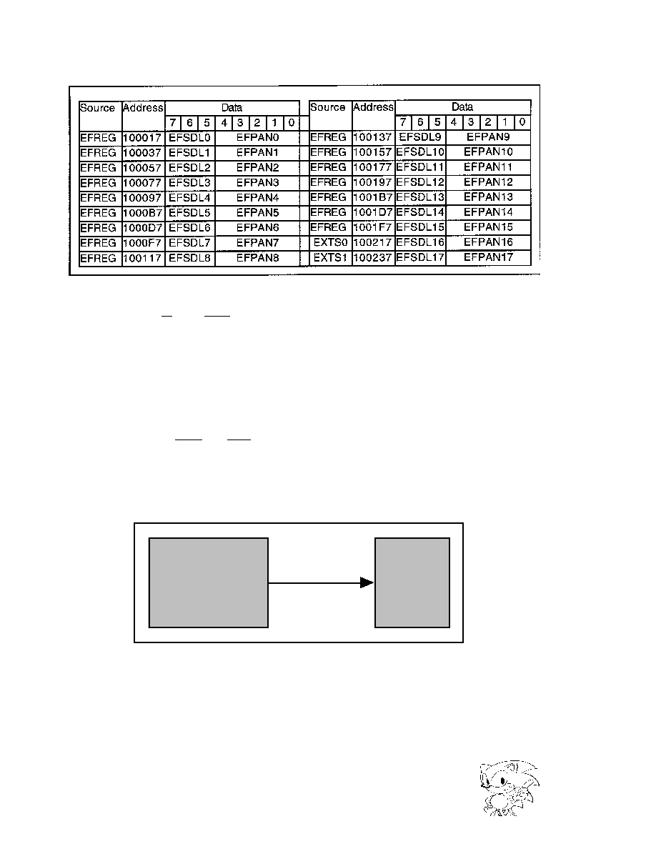
SEGA Confidential
Table 4.31 EFSDL, and EFPAN Register Addresses for Each EFREG and EXTS
MVOL[3:0] (W) ; Master VOLume
Represents the master volume output to the D/A con-
verter. Because it is used to control the overall output
level, lowering the "MVOL" for an output that has
overflowed to a lower level will not remove the clipping
noise. (To remove the clipping noise, correct the
"DISDL" and "EFSDL" settings to remove the overflow.)
DAC18B[3:0] (W) ; DAC out 18Bit
When setting the digital output as 18bit D/A converter
interface, set this bit to "1B". When 16 bit, set "0B." (Nor-
mally connected to an 16 bit type D/A converter so this
register should be set to "0B".)
SCSP
DAC
16bit format
Figure 4.57 SCSP and DAC Connections
88
|

SEGA Confidential
Slot Status Register
MSLC (w) ; Monitor SLot Call
Sets the number of the slot to be monitored with the
"CA" register. In "0
H
" it is "SLOT0", in "1F
H
" it is
"SLOT31"
CA (R) ; Call Address
The slot which has its number set in this register can read
out the number of samples (number of samples = the
number of wave form data samples) from the current
output waveform data "SA" (start address) address.
The value output here in the LSB (least significant bit)
indicates 4K (4096) samples, so when the output value is
"1
H
", the slots being monitored are outputting at least
more than "SA" to 4K samples of wave form addresses.
Sound Memory Configuration Register
MEM4MB (w) ; MEMory 4MBit
Designates the capacity of the memory connected to the
SCSP.
Table 4.32 Memory Size
000000
H
~01FFFF
H
000000
H
~03FFFF
H
When 1Mbit
1Mbit
1Mbit
4Mbit
4Mbit
4Mbit
(2nd)
(1st)
(2nd)
(1st)
000000
H
07FFFF
H
080000
H
0FFFFF
H
Figure 4.58 Memory Address Mapping Diagram
MIDI Register
The SCSP has a 31.25Kbps transfer rate MIDI serial interface, however, a MIDI
peripheral circuit and MIDI DIN connector are not included. As a result, MIDI
applications cannot be created. Figure 4.59 shows the MIDI interface block diagram.
MEM4MB
Memory Capacity
0
Uses 1Mbit DRAM
1
Uses 4Mbit DRAM
Saturn SCSP User's Manual
89
|

SEGA Confidential
1 Byte BUFFER
1 Byte BUFFER
1 Byte BUFFER
1 Byte BUFFER
M I D I- I N
1 Byte BUFFER
1 Byte BUFFER
1 Byte BUFFER
1 Byte BUFFER
M I D I- O U T
MIOVF
MIFULL
MIENP
MOFOLL
MOEMP
MIDI-IN
STATUS
MIDI-OUT
STATUS
S P Converter
P S Converter
SCSP Internal Data Bus
(S P Conversion: Serial
Parallel Conversion)
(P S Converter: Paralle
Serial Conversion)
Figure 4.59 MIDI-I/F Block Diagram
MIBUF[7:0] (R) ; Midi Input BUFfer
This is a MIDI input data buffer.
External data transferred into the MIDI-IN side is auto-
matically stored in the MIDI-IN buffer "MIBUF".
MIOVF (R) ; Midi Input OVer-Flow
When the MIDI-IN buffer is completely full of data and
more data is transferred to the MIDI-IN, "MIOVF"
changes to "1B" to indicate an overflow has taken place.
When an overflow happens, the MIDI communications
will not work correctly, causing a MIDI transmission
error.
MIFULL (R) ; Midi Input FULL
When all 4bytes of the MIDI-IN buffer is completely full
of data, the "MIFULL" will change to "1B" to indicate
that the buffer is full.
MIEMP (R) ; Midi Input EMPty
"1B" is set when the input FIFO is empty. When the
internal MIDI-IN buffer is emptied through the CPU, etc.,
reading data, and when there is nothing in the MIDI-IN
buffer, the "MIEMP" changes to "1B" to show that the
buffer is empty.
Figure 4.60 is a diagram of the MIDI-IN and the interrupt
generation block. Interrupts occur when the "MIEMP" is
"1B" and receives external data and changes to "0B".
When the MIDI-IN buffer is emptied through reading,
etc., and MIEMP changes back to 1B, then the interrupt is
released.
90
|
SEGA Confidential
Interrupt for the
MCPU (SCU)
Interrupt for the
SCPU (MC86EC000)
Interrupt Block
Interrupt flag
Interrupt command
M I D I Block
SCSP
MIEMP
MIFULL
MIOVF
Figure 4.60 MIDI IN Block and the Interrupt Generation Block
MOFULL (R) ; Midi Output FULL
When all 4bytes of the MIDI-OUT buffer is completely
full of data, the "MOFULL" will change to "1B" to indi-
cate that the buffer is full.
MOEMP (R) ; Midi Output EMPty
When all of the data in the MIDI-OUT buffer has been
sent out and no data is transferred into the MIDI buffer,
"MOEMP" changes to "1B" to indicate that the buffer is
empty. At the same time, an interrupt can be used to tell
the CPU that the buffer is empty. Figure 4.61 shows the
MIDI-OUT and interrupt generation block.
Interrupt for the
MCPU (SCU)
Interrupt for the
SCPU (MC68EC000)
Interrupt Block
Interrupt flag
Interrupt command
M I D I Block
SCSP
MOEMP
MOFULL
Figure 4.61 MIDI OUT Block and the Interrupt Generation Block
Saturn SCSP User's Manual
91
|

SEGA Confidential
MOBUF[7:0] (W) ; Midi Output BUFfer
This is a MIDI output data buffer. For MIDI-OUT-side
transfer, write data (to be transferred) into "MOBUF".
Afterwards, the data is automatically transferred.
Timer Register
The SCSP has three pre-scaler 8 bit up count timers: A, B and C. The pre-scaler
execute time is set individually by "TACTL", "TBCTL" and "TCCTL."
TACTL[2:0] (W) ; Timer-A ConTroL
Designates the increment cycle for timer A.
Table 4.33 Increment Cycle for Timer A
TBCTL[2:0] (W) ; Timer-B ConTroL
Designates the increment cycle for timer B.
Table 4.34 Increment Cycle for Timer B
TACTL
Increment Cycle
0
O n c e e v e r y s a m p l e
1
O n c e e v e r y 2 s a m p l e s
2
O n c e e v e r y 4 s a m p l e s
3
O n c e e v e r y 8 s a m p l e s
4
O n c e e v e r y 1 6 s a m p l e s
5
O n c e e v e r y 3 2 s a m p l e s
6
O n c e e v e r y 6 4 s a m p l e s
7
O n c e e v e r y 1 2 8 s a m p l e s
TBCTL
Increment Cycle
0
O n c e e v e r y s a m p l e
1
O n c e e v e r y 2 s a m p l e s
2
O n c e e v e r y 4 s a m p l e s
3
O n c e e v e r y 8 s a m p l e s
4
O n c e e v e r y 1 6 s a m p l e s
5
O n c e e v e r y 3 2 s a m p l e s
6
O n c e e v e r y 6 4 s a m p l e s
7
O n c e e v e r y 1 2 8 s a m p l e s
92
|
SEGA Confidential
TCCTL[2:0] (W) ; Timer-C ConTroL
Designates the increment cycle for timer C.
Table 4.35 Increment Cycle for Timer C
Table 4.36 shows the count cycle in relation to the setting values in
each of "TACTL", "TBCTL" and "TCCTL". Table 4.37 shows the
shortest interrupt time ("TIMA"="TIMB"="TIMC"="FEH") and
the longest interrupt time ("TIMA"="TIMB"="TIMC"="00H").
Table 4.36 Count Cycle in Relation to the Settings of TACTL, TBCTL and TCCTL
Table 4.37 Shortest and Longest Interrupt Time
TCCTL
Increment Cycle
0
O n c e e v e r y s a m p l e
1
O n c e e v e r y 2 s a m p l e s
2
O n c e e v e r y 4 s a m p l e s
3
O n c e e v e r y 8 s a m p l e s
4
O n c e e v e r y 1 6 s a m p l e s
5
O n c e e v e r y 3 2 s a m p l e s
6
O n c e e v e r y 6 4 s a m p l e s
7
O n c e e v e r y 1 2 8 s a m p l e s
TACTL, TBCTL, TCCTL
Values
Shortest Interrupt Time
[
µ
sec]
Longest Interrupt Time
[msec]
0 H
22.6757
5.8050
1 H
45.3515
11.6100
2 H
90.7029
23.2200
3 H
181.4059
46.4399
4 H
362.8118
92.8798
5 H
725.6236
185.7596
6 H
1451.2472
371.5193
7 H
2902.4943
743.0385
TACTL, TBCTL, TCCTL
Setting values
Count Cycle
(Compared with
1Fs=1/44.1K)
Actual Count Cycle Time
[
µ
sec]
0 H
F s
22.6757
1 H
F s/2
45.3515
2 H
F s/4
90.7029
3 H
F s/8
181.4059
4 H
F s/16
362.8118
5 H
F s/32
725.6236
6 H
F s/64
1451.2472
7 H
F s/128
2902.4943
Saturn SCSP User's Manual
93
|
SEGA Confidential
Based on Tables 4.36 and 4.37, the following equation can be used to find the inter-
rupt time.
Interrupt Time = {255 (FF
H
) TIMA (B, C) settings} X count cycle time
Counting begins immediately after the settings are set to "TIMA", "TIMB" and
"TIMC". When the count reaches FFH, an interrupt is sent from the timer valid for
an interrupt. (When the timer is not used, please prohibit the use of interrupt.)
TIMA[7:0] (W) ; TIMer-A count data
This is timer A. This timer is an up counter. When all of
the bits reach "1B" a request for an interrupt occurs.
TIMB[7:0] (W) ; TIMer-B count data
This is timer B. This timer is an up counter. When all of
the bits reach "1B" a request for an interrupt occurs.
TIMC[7:0] (W) ; TIMer-C count data
This is timer C. This timer is an up counter. When all of
the bits reach "1B" a request for an interrupt occurs.
94
|
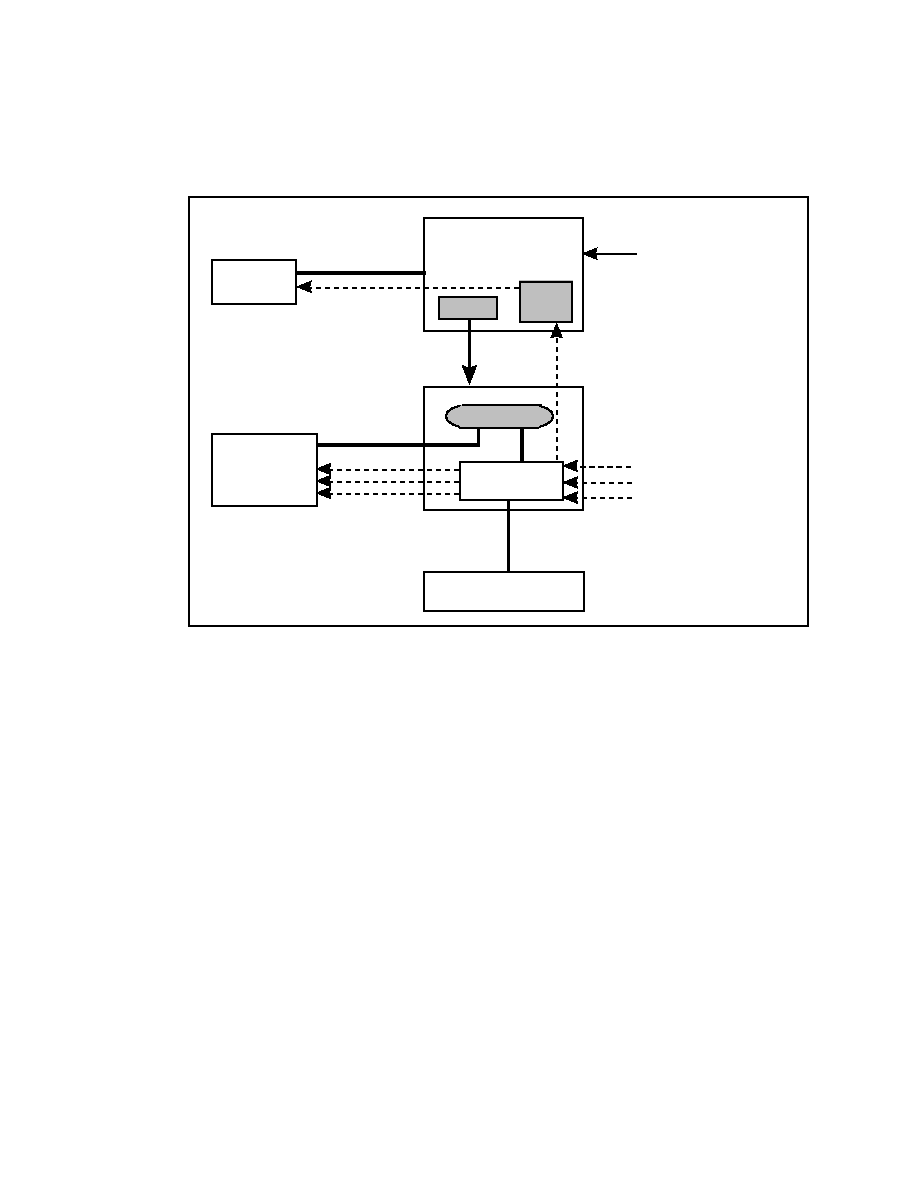
SEGA Confidential
Interrupt Control Register
The SCSP has an internal interrupt controller that includes functions that control the
interrupt signals for both the main CPU and the sound CPU.
SH-2
MC68EC000
SCIPL0~2
Interrupt Signal
External Interrupt Input
INT0N, INT1N, INT2N
(Currently not used)
4Mbit DRAM
DATA-BUS
SCSP
REGISTER
DMAC
B-BUS
(DMA)
MCINTN
(Interrupt Signal)
INTERRUPT
CONTROLLER
INTERRUPT
CONTROLLER
SCU
INT
(Interrupt Signal)
Figure 4.62 Sound Interrupt Signal Connections Diagram
The SCSP interrupt controller is at the center of the sound block interrupt signal
system and is connected to each CPU. Interrupt signals for the sound CPU have
levels 1 through 7 auto vector interrupts. Level setting of interrupts for the main
CPU cannot be set from the sound CPU side; vector settings also cannot be done.
Interrupts for the main CPU are not just interrupts, but can also be used as start
triggers for SCU DMA transfers. This function allows the timing of DMA transfers
of large data such as wave form data to be controlled through the sound CPU.
When using this function, set the main CPU (SCU, etc.) to send a sound interrupt to
start the DMA transfer in advance. (See the SCU user's manual for more detailed
information.)
Saturn SCSP User's Manual
95
|
SEGA Confidential
Registers are explained below. There are two types of registers: those that control
interrupts for the main (these have names that begins with MC~); and those that
control the interrupts for the sound (these have names that begins with SC~).
SCIPD[10:0] ; Sound-Cpu Interrupt PenDing
This register monitors the interrupts for the sound CPU
(interrupt flag). When an interrupt request occurs, the
appropriate interrupt request flag is set to "1
B
", so by
reading the CPU "SCIPD" register, it can be determined
which interrupt just occurred. Also, no matter what the
enable register ("SCIEB") is set at, all interrupt requests
are monitored. The corresponding flag can be reset by
the interrupt reset register ("SCIRE"). Only bit 5 can be
read or written; all others are read only. Writing "1B" to
bit 5 applies an interrupt to the sound CPU. However,
writing "0B" is invalid.
SCIEB[10:0] (R/W) ; Sound-Cpu Interrupt EnaBle
This register enables interrupts to the sound CPU. Set-
ting it to "1
B
" enables the corresponding hardware inter-
rupt. Reading "SCIPD" will determine whether there are
interrupts, regardless of the "SCIEB" setting. Setting to
"0
B
" is invalid
SCIRE[10:0] (W) ; Sound-Cpu Interrupt REset
This is the sound CPU, interrupt request reset flag.
When set to "1
B
", the corresponding hardware interrupt
is reset. (If the "SCIRE" for the bit with an interrupt
occurring is set to "1
B
", the "SCIPD" also will change
from "1
B
" to "0
B
".)
MCIPD[10:0] (R) ; Main-Cpu Interrupt PenDing
This register monitors the interrupts for the main CPU
(interrupt flag). When an interrupt request occurs, the
appropriate interrupt request flag is changed to "1B," so
by having the CPU read the "MCIPD" register, it can be
determined which interrupt just occurred. Also, all
interrupt requests are monitored regardless of what the
enable register ("MCIEB") is set to. The corresponding
flag can be reset by the interrupt reset register
("MCIRE"). Only bit 5 can be read or written; all others
are read only. Writing "1
B
" to bit 5 applies an interrupt to
the main CPU. However, writing "0B" is invalid.
96
|
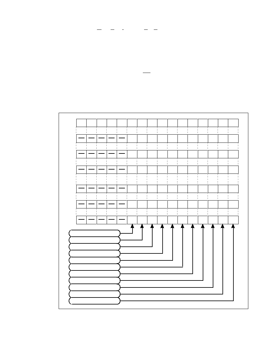
SEGA Confidential
MCIEB[10:0] (R) ; Main-Cpu Interrupt EnaBle
This register enables interrupts to the main CPU. Setting
it to "1B" enables the corresponding hardware interrupt.
Reading "MCIPD" determines whether there are inter-
rupts, regardless of the "MCIEB" setting. Setting to "0B"
is invalid.
MCIRE[10:0] (R) ; Main-Cpu Interrupt REset
This is the main CPU interrupt request reset flag. When
set to "1", the corresponding hardware interrupt request
is reset. (If the "MCIRE" for the bit with an interrupt
occurring is set to "1B", the "MCIPD" also will change
from "1B" to "0B".)
Figure 4.63 Interrupt Register Bit Accommodation
1 Sample (1Fs) Interrupt
b15 b14 b13 b12 b11 b10 b9
b8
b7
b6
b5
b4
b3
b2
b1
b0
RW RW RW RW RW RW RW RW RW RW RW
R
RW
R
R
R
R
R
R
R
R
R
W
W
W
W
W
W
W
W
W
W
W
W
W
W
W
W
W
W
W
W
W
W
R
RW
R
R
R
R
R
R
R
R
R
W
W
W
W
W
W
W
W
W
W
W
MIDI Output Interrupt
Timer C Interrupt
Timer B Interrupt
Timer A Interrupt
CPU Interrupt
DMA Transfer End Interrupt
MIDI Input Interrupt
External Interrupt "INT2N"
External Interrupt "INT1N"
External Interrupt "INT0N"
R: Read Only W: Write Only RW: Read and Write
SCIEB
SCIPD
SCIRE
MCIEB
MCIPD
MCIRE
Saturn SCSP User's Manual
97
|
SEGA Confidential
Table 4.38 Bit Factor Interrupt Registers
About SCILV0, 1, 2
This is the register that sets the auto vector interrupt level for the sound CPU.
Each register is partitioned in units of one bit per every interrupt factor. When
setting, view Figure 4.65 vertically.
In the example of bit 7, timers B, C and MIDI output interrupts, and the
interrupt level for each sample are all set at once. Level is set with a 3 bit code,
but each bit is distributed among SCILV0, 1 and 2.
MSB (upper)
SCILV2
SCILV1
SCILV0
4
2
1
LSB (lower)
Figure 4.64 3 Bit Code and Register Accommodation
The 3 bit code used to set the level is like Figure 4.64. For example, if it is set at
101
B
, the interrupt level is 5. "000
B
" is level 0 interrupt, so an interrupt would
not be applied.
However, the actual format of the register is shown in Figure 4.65. Be careful
when setting the values.
Bit
Reason for Interrupt
0
Applicable to the external interrupt input "INT0N" interrupt input.
1
Applicable to the external interrupt input "INT1N" interrupt input.
2
Applicable to the external interrupt input "INT2N" interrupt input.
3
Applicable to the MIDI input interrupt
I
nterrupt occurs when the MIDI-IN side FIFO buffer memory captures data from an empty state.
Automatic cancellation occurs when data is all read from the FIFO buffer and the buffer is empty.
4
Applicable to DMA transfer end interrupt
Interrupt occurs when the DMA transfer using the SCSP internal DMA is finished. (When data
transfer of the block set in "DLG" [length (volume)] is completely finished.)
5
Applicable to the CPU manual interrupt
By writing to the CPU (main or sound), an interrupt can be applied to the sound or main CPU.
Interrupt is applied when "1B" is written. ( "0B" is invalid.)
6
Applicable to a timer A interrupt
7
Applicable to a timer B interrupt
8
Applicable to a timer C interrupt
9
Applicable to the MIDI output interrupt
An interrupt request occurs when the MIDI-OUT side FIFO buffer memory becomes empty. The
interrupt is automatically cancelled when data is written into the MIDI-OUT buffer memory
(register) and it is no longer empty.
10
Applicable to one interrupt each sample (1 sample= 22.68
µ
sec= 1/44.1K intervals).
11~15 Invalid
98
|
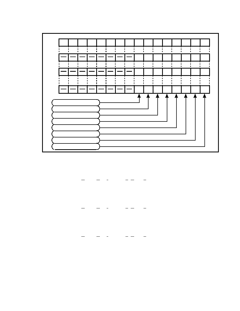
SEGA Confidential
Timer B, C & MIDI-OUT & 1Fs
b15 b14 b13 b12 b11 b10
b9
b8
b7
b6
b5
b4
b3
b2
b1
b0
W
W
W
W
W
W
W
W
W
W
W
W
W
W
W
W
W
W
W
W
W
W
W
W
Timer A
CPU Software Interrupt
DMA Transfer End
MIDI-IN
External Interrupt 2
SCILV0
SCILV1
SCILV2
External Interrupt 1
External Interrupt 0
SCILV0[7:0] (W) ;Sound-Cpu Interrupt LeVel bit0
Specifies bit0 of the sound CPU interrupt level code as
defined in bit application.
SCILV1[7:0] (W) ;Sound-Cpu Interrupt LeVel bit1
Specifies bit1 of the sound CPU interrupt level code as
defined in bit application.
SCILV2[7:0] (W) ;Sound-Cpu Interrupt LeVel bit2
Specifies bit2 of the sound CPU interrupt level code as
defined in bit application.
Figure 4.65 Format of the Interrupt Level Set Register
Saturn SCSP User's Manual
99
|

SEGA Confidential
Examples of interrupt settings are explained below.
Conditions:
Apply a level 6 interrupt to the sound CPU while timer A applies an
interrupt to the main CPU.
Procedure:
Currently, items without an interrupt applied set the timer after all of
the interrupt settings are finished, .
1:
Set the sound CPU interrupt level to 6
- Level 6 in the 3 bit code is "110
B
".
- The bit that controls timer A is bit 6, so set bit 6 in "SCILV0" to "0
B
".
(At 100425H address in byte, "00
H
", or at 100424H address in words "0000
H
".)
- Bit 6 in "SCILV0" to "1
B
".
(At 100427H address in byte, "40
H
", or at 100426H address in words "0040
H
".)
- Bit 6 in "SCILV0" to "1
B
".
(At 100429H address in byte, "40
H
", or at 100428H address in words "0040
H
".)
2:
Set parameters in registers "MCIEB" and "SCIEB" so that interrupts will be
applied to both the main and sound CPUs.
- Set bit 6 in register "MCIEB" to "1
B
" so that an interrupt will be applied by
timer A.
(At 10042B
H
address in byte, "40
H
", or at 10042A
H
address in words "0040
H
".)
- Set bit 6 in register "SCIEB" to "1
B
" so that an interrupt will be applied to
the sound CPU as well.
(At 100421
H
address in bytes, "40
H
", or at 10042E
H
address in words "0040
H
".)
- Furthermore, by setting the parameters in the timer, count will begin
immediately afterwards. When an overflow occurs, an interrupt will be
applied.
3:
Use the reset registers to remove the interrupts from either the sound or main
CPUs.
100
|
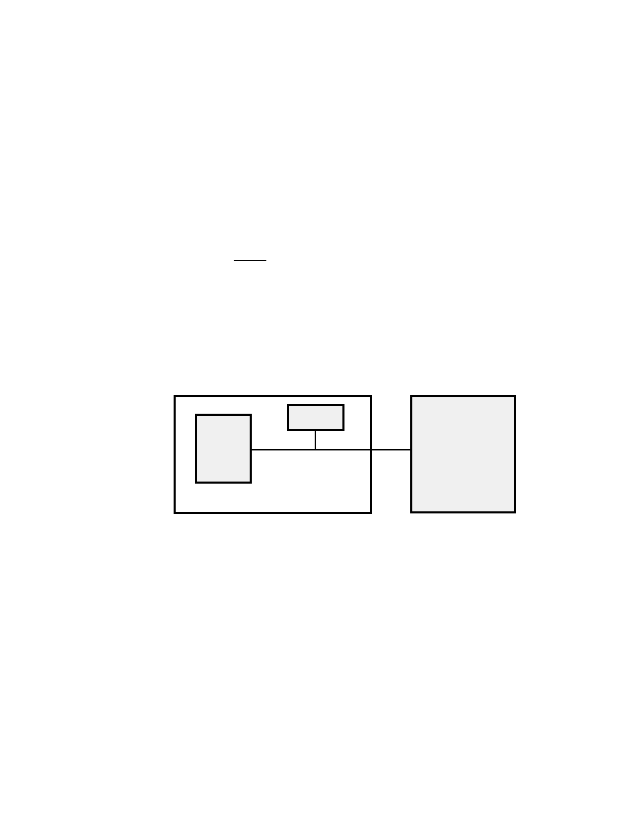
SEGA Confidential
DMA Transfer Register
The DMA inside the SCSP can only transfer between the SCSP internal control
register and the sound memory. From this the maximum bytes transferable is 3812
bytes (EE4H), (allocated in the empty memory from 100000H~100EE3H). Also, the
registers relating to the DMA cannot be changed with the DMA transfer.
During DMA transfer address continually move in the increase direction.
· The speed of the main CPU and sound CPU may drop during DMA transfer.
· Access through DMA transfer to the control register of the DMA controller is
absolutely prohibited. The operation when this transfer is performed is not
guaranteed at all.
· DMA transfer is word (16bit) transfer.
DGATE (R/W) ;Dma GATE (and "0")
The DMA controller block diagram is shown in Figure
4.66.
It can freely initialize the areas in the sound memory and
the SCSP internal control register to "0". When this bit is
"1B", "0" clear is executed (When actually starting,
"DEXE" must be executed).
Deleting DGATE transfer ("0" write) will not affect the
transfer source data. In addition, data will not be lost.
S C S P
CONTROL
REGISTER
DMAC
100000H
SOUND MEMORY
Internal data
Bus
100EE3H
~
~
000000H
0FFFFFH
Figure 4.66 DMA Controller Block Diagram
Saturn SCSP User's Manual
101
|

SEGA Confidential
DDIR (R/W) ; Dma (transferring) DIRection
Designates the DMA transfer direction. When this bit is
"0B", data is transferred from the sound memory to the
LSI block register; "1" transfers data in the opposite
direction.
Table 4.39 DMA Transfer Direction
DEXE (R/W) ; Dma EXEcution
Designates the start of the DMA transfer. When this bit is
"1", the DMA transfer starts. Writing "0" is invalid.
Also, when DMA transfer ends, this bit is automatically
reset to "0".
Table 4.40 DMA Transfer
DMEA[19:1] (W) ; Dma MEmory start Address
Designates the sound memory address (word units) that
starts the DMA transfer.
DRGA[11:1] (W) ; Dma ReGister start Address
Designates the block register byte address in the LSI
(word units) that starts the DMA transfer.
DTLG[11:1] (W) ; Dma (Transferring) LenGth
Designates the word count being transferred during
DMA transfer. At that time, be careful that the area of the
transfer origin or destination does not exceed the area of
the sound memory area or the LSI internal block register
area.
DEXE
Transfer Status
0
Invalid or transfer has ended
1
Starts DMA transfer
DDIR
Transfer Direction
0
From sound memory to LSI internal register
1
From LSI internal register to sound memory
102
|
SEGA Confidential
4.3
DSP Memory Control Register
RBL[1:0] (W) ; Ring Buffer Length
Designates the length of the ring buffer.
Table 4.41 RBL and the Ring Buffer Length
RBP[19:13] (W) ; Ring Buffer (header) Pointer
Designates the first address of the ring buffer. This
address designation is per 4K-word boundary.
The important base of DSP effect processing is delay
processing. Delay is accomplished by storing the input
data in memory and reading it out again after a certain
time lag is applied. This storage area is called the ring
buffer.
By combining the number of effect programs used and
the effect delay timer used simultaneously, the ring
buffer area settings can be set to perform the "RBL" and
"RBP" registers.
bit
Buffer Length
0
8K word
1
16K word
2
32K word
3
64K word
Saturn SCSP User's Manual
103
|

SEGA Confidential
104
|

SEGA Confidential
Chapter 5
SCSP Internal DSP Operation
Chapter 5 Contents
5.1 DSP Configuration
106
5.2 DSP Internal RAM
107
Saturn SCSP User's Manual
105
Chapter 5 Contents
5.1 DSP Configuration ..................................... 106
5.2 DSP Internal RAM ...................................... 107
|
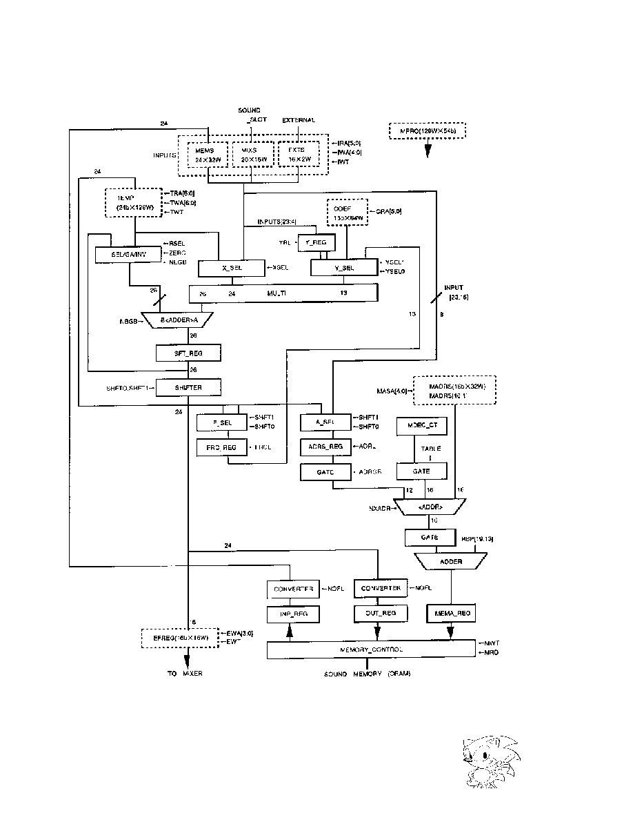
SEGA Confidential
5.1
DSP Configuration
Figure 5.1 DSP Configuration Diagram
106
|

SEGA Confidential
5.2
DSP Internal RAM
EXTS[15:0] ; EXTernal Stack
Represents the digital audio input data buffer. (This
register cannot be accessed.)
MIXS[19:0] (R/W) ; MIX Stack
Represents the sound data buffer from the input mixer.
MEMS[23:0] (R/W) ; MEMory Stack
Represents the input data buffer from the sound memory.
TEMP[23:0] (R/W) ; TEMPorary register
Represents the DSP work buffer (128 words). The DSP
work buffer is in ring buffer configuration, the pointer
decreases at every sample.
COEF[12:0] (R/W) ; COEFficient register
Represents the DSP coefficient buffer.
MADRS[16:1] (R/W) ; Memory ADdReSs register
Represents the DSP address buffer.
MPRO[63:0] (R/W) ; Micro PROgram register
Represents the DSP micro program buffer.
EFREG[15:0] (R/W) ; EFfect REGister
Represents the DSP output buffer.
Saturn SCSP User's Manual
107
|