
SEGA Confidential
General Notice
When using this document, keep the following in mind:
1. This document is confidential. By accepting this document you acknowledge that you are bound
by the terms set forth in the non-disclosure and confidentiality agreement signed separately and /in
the possession of SEGA. If you have not signed such a non-disclosure agreement, please contact
SEGA immediately and return this document to SEGA.
2. This document may include technical inaccuracies or typographical errors. Changes are periodi-
cally made to the information herein; these changes will be incorporated in new versions of the
document. SEGA may make improvements and/or changes in the product(s) and/or the
program(s) described in this document at any time.
3. No one is permitted to reproduce or duplicate, in any form, the whole or part of this document
without SEGA'S written permission. Request for copies of this document and for technical
information about SEGA products must be made to your authorized SEGA Technical Services
representative.
4. No license is granted by implication or otherwise under any patents, copyrights, trademarks, or
other intellectual property rights of SEGA Enterprises, Ltd., SEGA of America, Inc., or any third
party.
5. Software, circuitry, and other examples described herein are meant merely to indicate the character-
istics and performance of SEGA's products. SEGA assumes no responsibility for any intellectual
property claims or other problems that may result from applications based on the examples
describe herein.
6. It is possible that this document may contain reference to, or information about, SEGA products
(development hardware/software) or services that are not provided in countries other than Japan.
Such references/information must not be construed to mean that SEGA intends to provide such
SEGA products or services in countries other than Japan. Any reference of a SEGA licensed prod-
uct/program in this document is not intended to state or simply that you can use only SEGA's
licensed products/programs. Any functionally equivalent hardware/software can be used instead.
7. SEGA will not be held responsible for any damage to the user that may result from accidents or any
other reasons during operation of the user's equipment, or programs according to this document.
(6/27/95- 002)
NOTE: A reader's comment/correction form is provided with this
document. Please address comments to :
SEGA of America, Inc., Developer Technical Support (att. Evelyn Merritt)
150 Shoreline Drive, Redwood City, CA 94065
SEGA may use or distribute whatever information you supply in any way
it believes appropriate without incurring any obligation to you.
|

SEGA Confidential
TM
© 1994 SEGA. All Rights Reserved.
VDP2
User's Manual
Version 1.1
Doc. #ST-58-R2-060194
|

SEGA Confidential
READER CORRECTION/COMMENT SHEET
Chpt.
pg. #
Correction
Corrections:
General Information:
Your Name
Phone
Document number
Date
Document name
Questions/comments:
Keep us updated!
If you should come across any incorrect or outdated information while reading through the attached
document, or come up with any questions or comments, please let us know so that we can make the
required changes in subsequent revisions. Simply fill out all information below and return this form to
the Developer Technical Support Manager at the address below. Please make more copies of this form if
more space is needed. Thank you.
Fax:
(415) 802-3963
Attn: Manager,
Developer Technical Support
Mail:
SEGA OF AMERICA
Attn: Manager,
Developer Technical Support
275 Shoreline Dr. Ste 500
Redwood City, CA 94065
Where to send your corrections:
ST-58-R2-060194
VDP2 User's Manual
|

SEGA Confidential
REFERENCES
In translating/creating this document, certain technical words and/or phrases were interpreted
with the assistance of the technical literature listed below.
1.
KenKyusha New Japanese-English Dictionary
1974 Edition
2.
Nelson's Japanese-English Character Dictionary
2nd revised version
3.
Microsoft Computer Dictionary
4.
Japanese-English Computer Terms Dictionary
Nichigai Associates
4th version
|

SEGA Confidential
Preface
This manual describes the VDP2 (Video Display Processor 2) and how to use it. The VDP2
controls the scroll screen control and the display priority control.
Manual Notations
Notations within this manual are described below.
Binary, hexadecimal
Binary notation has a B attached at the end (as in 100B); however, B may be omitted when
binary notation is obvious. Hexadecimal notation has an H attached at the end (as in 00H
and FFH).
Units
1 Kbyte is 1024 bytes. 1 Mbit is 1024 Kbits, or 1,048,576 bits.
MSB, LSB
The structure of byte and word shows the MSB (most significant bit) on the left and LSB (least
significant bit) on the right.
An undefined bit
A bit not defined by the register is shown as a dash. A "0" should be written into an undefined
bit of the register. Bits not defined by data of tables defined by VRAM are shown as shaded.
As a rule, a 0 should be written, providing that the undefined bit is ignored.
Byte, word, bit
Bits, as in digits of 0 and 1, are the lowest unit of data. A byte consists of 8 bits. A word consists
of 2 bytes, and begins from an even address.
Boundary
A boundary defines data from an address divisible by a selected value. For example, data for a
20H-byte boundary is defined at addresses beginning from 20H, 40H, and so on. A word is a
2-byte boundary.
Address
All addresses defined by VDP2 are relative addresses within VDP2. The first address of VDP2
begins from 5E00000H. For example, VRAM is at 000000H address of the relative address, and
begins from 5E00000H address of the absolute address. The TV screen mode register is at
180000H address of the relative address, and is set at address 5F80000H of the absolute address.
i
|

SEGA Confidential
Manual Structure
The main items described in each chapter are as follows.
Table 1.
Chapters and Main Items
ii
Chapter Name
Contents
Chapter 1 VDP2 Functions
VDP2 Functions
Chapter 2 TV Screen
TV Screen Mode, Normal, Hi-Res, Exclusive
Monitor, Interlace Mode, External Signal, H
-
Counter, V-Counter, Exclusive Hi-Res Setting
Chapter 3 RAM
VRAM Size, Address Map, VRAM, Color RAM,
Register, VRAM Change, VRAM Bank
Partition, VRAM Access Method, Color RAM
Mode
Chapter 4 Scroll Screen
Cell, Character Color Count, Transparent Dot,
Character Pattern, Pattern Name Table,
Special Function Bit, Reverse Function Bit,
Page, Plane, Map, Bitmap, Screen-Over
Process, Mosaic Process
Chapter 5 Normal Scroll Screen
Screen Scroll, Scaling, Line Scroll, Vertical Cell
Scroll Coordinates
Chapter 6 Rotation Scroll Screen
Rotation Scroll Increment, Rotation Scroll
Screen Display, Rotation Parameter
Coefficient Table
Chapter 7 Line Screen
Line Color Screen, Back Screen
Chapter 8 Window
Normal Rectangular Window, Normal Line
Window, Sprite Window
Chapter 9 Sprite Data
Sprite Type, Sprite Color Mode, Priority, Color
Calculation
Chapter 10 Dot Color Data
Palette Format, RGB Format, Sprite Dot, Scroll
Dot, Special Function Code
Chapter 11 Priority Function
Priority Number, Line Color Screen Insertion
Chapter 12 Color Calculation
Color Calculation, Extended Color Calculation,
Special Color Calculation, Gradation
Calculation
Chapter 13 Color Offset Function
Color Offset
Chapter 14 Shadow Function
Normal Shadow, MSB Shadow
Chapter 15 How To Use VDP2
Operation Flow Chart, How to use RAM, Bit
Structure
|

SEGA Confidential
Function
Details
Chapter
Overview
~
1
VDP2 Functions
TV Screen Configuration, Designate Display
Area, Boarder Area
2.1
TV Screen Configuration
TV Screen
TV Screen Mode, Normal, Hi-Res, Exclusive
Monitor
2.2
TV Screen Mode
Interlace, Non-interlace, Single-Density Interlace,
Double-Density Interlace
2.3
Interlace Mode
Address Map
3.1
Address Map
Size
3.1
Address Map
RAM
VRAM
Change
3.2
VRAM Change
Bank Partition
3.3
VRAM Bank Partition
Access During Display
3.4
How to Access VRAM
During Display
Color RAM Mode
3.5
Color RAM Mode
Screen Display
4.1
Screen Display Control
Character
Color Count
Bitmap Color
Count
4.3
Cell
Color
Palette Format
Dot Color Data
10.1
Palette Format Dot Color
Data
Normal Scroll
Screen
RGB Format
Dot Color Data
10.2
RGB Format Dot Color Data
Scroll Screen
Rotation Scroll
Screen
Color RAM
Mode
3.5
Color RAM Mode
Cell
4.3
Cell
Character
Pattern
4.4
Character Pattern
Cell Format
Pattern Name
Table (Page)
4.6
Pattern Name Table (Page)
Plane
4.7
Plane
Map
4.8
Map
Bitmap Format
4.9
Bitmap
Display Area, Screen-Over
4.10
Display Area
Mosaic Process
4.11
Mosaic Process
Screen Scroll Function
5.1
Screen Scroll Function
Scale Function
5.2
Scale Function
Line Scroll Function, Vertical
Cell Scroll Function
5.3
Line & Vertical Cell Scroll
Function
iv
Table 2.
Functions, their chapters and sections
|

SEGA Confidential
v
Function
Details
Chapter
Coordinates Calculation
6.1
Rotation Scroll Coordinates
Calculation
Rotation
Display Control
6.2
Rotation Scroll Screen
Display Control
Scroll Screen
Rotation Parameter Control
6.3
8
Rotation Parameter Control
Window
Scroll Screen
Coefficient Control
6.4
Coefficient Table Control
Line Screen
Line Color Screen
7.1
6.4
11.3
Line Color Screen
Coefficient Table Control
Line Color Screen Insertion
Back Screen
7.2
Back Screen
Window
Normal Rectangular Window, Normal Line
Window, Sprite Window, Window Effective Area
8
9.1
Window
Sprite Data
Sprite Data, Type, Color Mode
9.1
Sprite Data
Priority and Color Calculation
9.2
Priority and Color
Calculation
Sprite
Sprite Window
8
9.1
Window
Sprite Data
Dot Color
Palette Format
10.1
Palette Format Dot Color
Data
Data
RGB Format
10.2
RGB Format Dot Color Data
Color RAM Mode
3.5
Color RAM Mode
Priority Function
11.1
9.2
Priority Function
Priority and Color
Calculation
Priority
Special Priority Function
11.2
10.3
Special Priority Function
Special Function Code
Line Color Screen Insertion
11.3
7.1
Line Color Screen Insertion
Line Color Screen
Color Calculation Function,
Extended Color Calculation
Function
12.1
7.1
Color Calculation Function
Line Color Screen
Image Process
Color
Special Color Calculation
Function
12.3
10.3
Special Color Calculation
Function
Special Function Code
Gradation Calculation Function 12.2
Gradation Calculation
Function
Color Calculation Window
8
Window
Color Offset Function
13
Color Offset Function
Shadow
Normal Shadow, MSB Shadow 14
9.1
Shadow Function
Sprite Data
Table 2.
Functions, their chapters and sections (continued)
|

SEGA Confidential
vi
Table of Contents
Preface ............................................................................................................................ i
Manual Notation .................................................................................................. i
Manual Structure ............................................................................................... iii
List of Figures................................................................................................................ xi
List of Tables ............................................................................................................... xiv
Chapter 1 VDP2 Functions ........................................................................................... 1
Introduction......................................................................................................... 2
1.1 System Configuration ................................................................................... 2
1.2 Address Map ................................................................................................ 3
VRAM ..................................................................................................... 3
Color RAM .............................................................................................. 3
Register .................................................................................................. 4
1.3 Scroll Function.............................................................................................. 5
Display Screen ....................................................................................... 5
Scroll Screen .......................................................................................... 6
Line Screen ............................................................................................ 7
Windows ................................................................................................. 7
1.4 Priority Function ........................................................................................... 8
Priority Function ...................................................................................... 8
Color Calculation Function ..................................................................... 8
Color Offset Function .............................................................................. 8
Shadow Function .................................................................................... 9
Chapter 2 TV Screen .................................................................................................. 11
2.1 TV Screen Mode ........................................................................................12
Special High Resolution Graphic Mode ................................................ 13
2.2 Interlace Mode............................................................................................ 14
2.3 TV Screen Structure ................................................................................... 15
2.4 TV Screen Mode Register .......................................................................... 16
2.5 External Signals and Scan Conditions ....................................................... 19
External Signal Enable Register ........................................................... 19
Screen Status Register ........................................................................ 21
H Counter Register ............................................................................... 23
V Counter Register ............................................................................... 24
Chapter 3 RAM ...........................................................................................................25
Introduction....................................................................................................... 26
3.1 Address Map .............................................................................................. 26
VRAM Size Register ............................................................................. 28
3.2 VRAM Bank Partitioning ............................................................................. 29
RAM Control Register .......................................................................... 29
3.3 Accessing VRAM During Display Interval .................................................. 31
VRAM Access During Display Interval ................................................. 31
I
mage Data Access ..............................................................................32
Vertical Cell Scroll Table Data Access .................................................. 35
Read/Write Access by the CPU ............................................................ 35
VRAM Cycle Pattern Selection Process ............................................... 37
|

SEGA Confidential
VRAM Cycle Pattern Register .............................................................. 39
3.4 Color RAM Mode ........................................................................................ 43
RAM Control Register .......................................................................... 45
Chapter 4 Scroll Screen .............................................................................................. 47
4.1 Screen Display Control .............................................................................. 48
Screen Display Enable Register ........................................................... 48
4.2 Scroll Screen Structure .............................................................................. 50
Cell Format ....................................................................................................... 50
Bit Map Format ................................................................................................. 52
4.3 Cell ............................................................................................................. 53
Character Color Number ...................................................................... 53
Cell Data Configuration ........................................................................ 53
Transparent Dots .................................................................................. 57
RGB Format Dot Data .......................................................................... 58
4.4 Character Patterns ..................................................................................... 59
Character Size and Cell Arrangement .................................................. 59
4.5 Character Control Register ........................................................................ 60
4.6 Pattern Name Table (Page) ........................................................................ 64
Pattern Name Table Data Configuration ............................................... 64
Pattern Name Data ............................................................................... 69
Character Number ................................................................................ 74
Palette Number ..................................................................................... 74
Special Function Bit .............................................................................. 74
Reverse (Flip) Function Bit ................................................................... 75
Pattern Name Control Register ............................................................ 76
4.7 Planes ........................................................................................................ 79
Plane Size ............................................................................................ 79
Plane Size Register .............................................................................. 80
4.8 Maps ........................................................................................................... 82
Map Selection Register ........................................................................ 82
Map Size ............................................................................................... 84
Map Offset Register .............................................................................. 85
Normal Scroll Screen Map Register ..................................................... 87
Rotation Scroll Surface Map Register .................................................. 89
4.9 Bit Maps ..................................................................................................... 93
Bit Map Size ......................................................................................... 93
Bit Map Color Number .......................................................................... 93
Bit Map Pattern ..................................................................................... 95
Bit Map Palatte Number ..................................................................... 111
Special Function Bit ............................................................................ 111
Bit Map Palatte Number Register ....................................................... 112
4.10 Display Area ........................................................................................... 114
Display Area ....................................................................................... 114
Screen-Over Process ......................................................................... 115
Display-Over Pattern Name ............................................................... 115
Screen-Over Pattern Name Register ................................................. 116
4.11 Mosaic Process ...................................................................................... 117
Mosaic Control Register ..................................................................... 118
vii
|

SEGA Confidential
Chapter 5 Normal Scroll Screen ............................................................................... 121
Introduction..................................................................................................... 122
5.1 Screen Scroll Function ............................................................................. 122
Screen Scroll Value Register .............................................................. 123
5.2 Expansion/Contraction Function .............................................................. 126
Coordinate Increment Register .......................................................... 127
Reduction Enable Register ................................................................. 129
5.3 Line and Vertical Cell Scroll Function ....................................................... 131
Line Scroll Function ............................................................................ 131
Vertical Cell Scroll Function ................................................................ 134
Line and Vertical Cell Scroll Control Register ..................................... 137
Line Scroll Table Address Register ..................................................... 140
Vertical Cell Scroll Table Address Register ........................................ 141
Chapter 6 Rotation Scroll Screen ............................................................................. 143
Introduction..................................................................................................... 144
6.1 Rotation Scroll Coordinate Operation ...................................................... 144
6.2 Rotation Scroll Screen Display Control .................................................... 148
RAM Control Register ........................................................................ 148
6.3 Rotation Parameter Control ..................................................................... 151
Data Configuration of the Rotation Parameter Table .......................... 153
Rotation Parameter Table ................................................................... 155
Rotation Parameter Read Control Register ........................................ 157
Rotation Parameter Table Address Register ...................................... 158
Rotation Read Out of the Frame Buffer .............................................. 159
Rotation Parameter Change ............................................................... 160
Rotation Parameter Mode Register .................................................... 162
6.4 Coefficient Table Control .......................................................................... 163
Line Color Screen Data ...................................................................... 164
Bit Configuration of Coefficient Table Data ......................................... 165
Coefficient Table Lead Address .......................................................... 165
Most Significant Bit of Coefficient Data .............................................. 166
RAM Control Register ........................................................................ 167
Coefficient Table Control Register ...................................................... 168
Coefficient Table Address Offset Register .......................................... 170
Chapter 7 Line Screen .............................................................................................. 171
Introduction..................................................................................................... 172
7.1 Line Color Screen .................................................................................... 172
Line Color Screen Table Address Register ......................................... 174
7.2 Back Screen ............................................................................................. 175
Back Screen Table Address Register ................................................. 176
Chapter 8 Windows ................................................................................................... 179
8.1 Window Area ............................................................................................ 180
Normal Rectangular Window .............................................................. 180
Window Position Register .................................................................. 181
Normal Line Window .......................................................................... 184
Line Window Table Address Register ................................................. 186
Sprite Window .................................................................................... 187
viii
|

SEGA Confidential
Sprite Control Register ....................................................................... 188
Window's Active Area for the Screen.................................................. 189
8.2 Window Process .......................................................................................190
Window Control Register .................................................................... 193
Chapter 9 Sprite Data ...............................................................................................199
9.1 Sprite Data ...............................................................................................200
Sprite Types ........................................................................................ 200
Sprite Color Mode............................................................................... 203
9.2 Priority and Color Calculation ................................................................... 204
Priority Number Selection ................................................................... 204
Color Calculation Enable Conditions .................................................. 205
Color Calculation Ratio Selection ....................................................... 206
Sprite Control Register ....................................................................... 207
Priority Number Register .................................................................... 209
Color Calculation Ratio Registers ...................................................... 210
Chapter 10 Pixels ...................................................................................................... 213
Introduction..................................................................................................... 214
10.1 Palette Format Pixels ............................................................................. 214
Sprite Dot Pixels ................................................................................. 214
Scroll Dot Pixels ................................................................................. 216
Color RAM Address Offset Register ................................................... 217
10.2 RGB Format Pixels ................................................................................ 218
Sprite Pixels........................................................................................ 218
Scroll Pixels ........................................................................................ 218
10.3 Special Function Code ........................................................................... 220
Special Function Code Select Register .............................................. 221
Special Function Code Register ......................................................... 222
Chapter 11 Priority Function ......................................................................................223
Introduction..................................................................................................... 224
11.1 Priority Function ......................................................................................224
Priority Number ................................................................................... 224
Priority Number Register .................................................................... 225
11.2 Special Priority Function ......................................................................... 227
Special Priority Mode Register ........................................................... 229
11.3 Insertion of Line Color Screen ............................................................... 230
Line Color Screen Enable Register .................................................... 231
Chapter 12 Color Calculations ................................................................................... 233
Introduction..................................................................................................... 234
12.1 Color Calculation Function ..................................................................... 234
Normal Color Calculation ................................................................... 234
Extended Color Calculation Function ................................................. 236
12.2 Gradation Calculation Function .............................................................. 238
Color Calculaton Control Register ...................................................... 240
Color Calculation Ratio Register ........................................................ 243
12.3 Special Color Calculation Function ........................................................ 245
Special Color Calculation Mode Register ........................................... 247
ix
|

SEGA Confidential
Chapter 13 Color Offset Function ............................................................................. 249
Introduction..................................................................................................... 250
13.1 Color Offset Selection ............................................................................ 250
Color Offset Enable Register .............................................................. 251
Color Offset Select Register ............................................................... 252
Color Offset Register .......................................................................... 253
Chapter 14 Shadow Function ................................................................................... 255
Introduction..................................................................................................... 256
14.1 Shadow Process .................................................................................... 256
Normal Shadow .................................................................................. 256
MSB Shadow ......................................................................................258
Shadow Control Register ................................................................... 259
Chapter 15 How to Use VDP2 .................................................................................. 261
15.1 Operation Flow ....................................................................................... 262
15.2 How to Use RAM .................................................................................... 264
15.3 Bit Configuration Map ............................................................................. 267
Chapter 16 Quick Reference .................................................................................... 295
16.1 Register Map .......................................................................................... 296
16.2 Register Bit List ......................................................................................315
16.3 Register Bit Functions ............................................................................ 328
16.4 Table List ................................................................................................389
x
|

SEGA Confidential
Table of Figures
Chapter 1 VDP2 Functions
Figure 1.1 System Configuration ........................................................................ 2
Figure 1.2 Address Map ..................................................................................... 3
Chapter 2 TV Screen
Figure 2.1 Display Method by Interlace Setting ............................................... 14
Figure 2.2 TV Screen Structure........................................................................ 15
Chapter 3 RAM
Figure 3.1 Different Capacities of VRAM Address Map ................................... 27
Figure 3.2 VRAM Cycle Pattern Register ......................................................... 32
Figure 3.3 Access Selection Limits of Pattern Name Table Data ..................... 33
Figure 3.4 Example of Character Pattern Data Read Access
Selection ......................................................................................... 34
Figure 3.5 Access Select Limits of Vertical Cell Scroll Table Data ................... 35
Figure 3.6 CPU Read/Write Access Selection when
VRAM is not Divided into Two Bank ............................................... 36
Figure 3.7 CPU Read/Write Access Selection when
VRAM is Divided into Two Banks ................................................... 37
Figure 3.8 VRAM Cycle Pattern Selection ....................................................... 39
Figure 3.9 Color Data Configuration on Color RAM ......................................... 44
Figure 3.10 Color Data of the Color RAM ........................................................ 45
Chapter 4 Scroll Screen
Figure 4.1 Scroll Screen Configuration of Cell Format ..................................... 50
Figure 4.2 Scroll Screen Configuration of Cell Format and
Corresponding Data Settings ......................................................... 51
Figure 4.3 Scroll Screen Configuration of Bit Map Format............................... 52
Figure 4.4 Relationship of bit map format scroll screen and data settings ....... 52
Figure 4.5 Configuration of Cells by Character Color Count ............................ 54
Figure 4.6 RGB Format Dot Data ..................................................................... 58
Figure 4.7 Cell Arrangement by Character Size ............................................... 59
Figure 4.8 Data Configuration of Pattern Name Tables ................................... 65
Figure 4.9 Bit Configuration when Pattern Name Data is 2 Word .................... 69
Figure 4.10 Configuration when Pattern Name Data is 1 Word ....................... 71
Figure 4.11 Dot Color Data by Character Number of Colors ............................ 74
Figure 4.12 Reverse Display of Character Patterns ......................................... 75
Figure 4.13 Arrangement of Pattern Name Table by Plane Size ...................... 79
Figure 4.14 Map Selection Register ................................................................. 82
Figure 4.15 Map Size ....................................................................................... 84
Figure 4.16 Plane Arrangement of Map by Reduction Settings ....................... 85
Figure 4.17 Bit Map Pattern Configuration ....................................................... 96
Figure 4.18 Dot Color Data by Bit Map Number of Colors ............................. 111
Figure 4.19 Mosaic Pattern ............................................................................ 117
xi
|

SEGA Confidential
Chapter 5 Normal Scroll Screen
Figure 5.1 Screen Scroll Value Bit Configuration ........................................... 122
Figure 5.2 Configuration of Coordinate Increment Register........................... 126
Figure 5.3 Line Scroll Function ...................................................................... 131
Figure 5.4 Bit Configuration of Line Scroll Table Data ................................... 132
Figure 5.5 Line Scroll Table ............................................................................ 133
Figure 5.6 Vertical Cell Scroll Function .......................................................... 134
Figure 5.7 Data Configuration on Vertical Cell Scroll Table ........................... 135
Figure 5.8 Vertical Cell Scroll Table................................................................ 136
Chapter 6 Rotation Scroll Screen
Figure 6.1 Rotation Scroll Screen Display Method ........................................ 145
Figure 6.2 Rotation Parameter data Configuration ........................................ 153
Figure 6.3 Rotation Parameter Table ............................................................. 156
Figure 6.4 How to Store to the Rotation Parameter Table VRAM .................. 157
Figure 6.5 Rotation Parameter Change ......................................................... 161
Figure 6.6 Line Color Screen Data Using Coefficient Data ............................ 164
Figure 6.7 Bit Configuration of Coefficient Table Data ................................... 165
Chapter 7 Line Screen
Figure 7.1 Line Screen ................................................................................... 172
Figure 7.2 Configuration of Line Color Screen Table ..................................... 173
Figure 7.3 Bit Configuration of Line Color Screen Table Data ....................... 173
Figure 7.4 Configuration of Back Screen Table .............................................. 175
Figure 7.5 Bit Configuration of Back Screen Table Data ................................ 176
Chapter 8 Windows
Figure 8.1 Normal Rectangle Window ........................................................... 180
Figure 8.2 Normal Line Window ..................................................................... 184
Figure 8.3 Bit Configuration of Normal Line Window Table Data ................... 184
Figure 8.4 Configuration of Normal Line Window Table ................................. 185
Figure 8.5 Sprite Window ............................................................................... 187
Figure 8.6 Active Area of Windows ................................................................ 189
Figure 8.7 Window Process ........................................................................... 191
Chapter 9 Sprite Data
Figure 9.1 Sprite Types .................................................................................. 201
Chapter 10 Dot Color Data
Figure 10.1 Palette Format Sprite Dot Color Data ......................................... 215
Figure 10.2 Sprite Color RAM Address .......................................................... 215
Figure 10.3 Palette Format Scroll Dot Color Data .......................................... 216
Figure 10.4 Scroll Color RAM Address .......................................................... 216
Figure 10.5 RGB Format Sprite Dot Color Data ............................................. 218
Figure 10.6 RGB Format Scroll Dot Color Data ............................................. 219
Figure 10.7 Dot Color Code Corresponding to Special Function Code ......... 220
xii
|

SEGA Confidential
Chapter 11 Priority Function
Figure 11.1 Priority Function .......................................................................... 224
Figure 11.2 Line Color Screen Insertion ......................................................... 230
Chapter 12 Color Operations
Figure 12.1 Color Calculation Function ......................................................... 234
Figure 12.2 Color Calculation Ratio Mode ..................................................... 236
Figure 12.3 Expand Color Operation Function ............................................... 237
Figure 12.4 Gradation Calculation Function ................................................... 239
Chapter 13 Color Offset Function
Figure 13.1 Color Offset Data ........................................................................ 250
Chapter 14 Window Function
Figure 14.1 Shadow Function ........................................................................ 256
Figure 14.2 Sprite Data Write of a Normal Shadow ....................................... 257
Figure 14.3 Sprite Data of a Normal Shadow ................................................ 257
Figure 14.4 Sprite Shadow and Transparent Shadow ................................... 258
Figure 14.5 Sprite Data of MSB Shadow ....................................................... 259
xiii
|

SEGA Confidential
List of Tables
Chapter 1 VDP2 Functions
Table 1.1 TV Screen Mode ................................................................................. 5
Table 1.2 Scroll Screen ..................................................................................... 5
Table 1.3 Windows ............................................................................................. 6
Table 1.4 Scroll Screen Function ....................................................................... 6
Chapter 2 TV Screen
Table 2.1 TV Screen Mode ............................................................................... 12
Table 2.2 Register for Setting the External Screen .......................................... 21
Table 2.3 H Counter Register Bit Content ........................................................ 24
Table 2.4 V Counter Register Bit Content ........................................................ 24
Chapter 3 RAM
Table 3.1 Data Defined in VRAM ..................................................................... 26
Table 3.2 Access Numbers of Required Pattern Name Table Data
during 1 Cycle .................................................................................. 33
Table 3.3 Character Pattern Data (Bit Map Pattern Data)
Read Access Number ...................................................................... 34
Table 3.4 Character Pattern Data Read Access Selection Limits .................... 34
Table 3.5 Access Command ............................................................................. 40
Chapter 4 Scroll Screen
Table 4.1 Character Color Count and Dot Data Size ....................................... 53
Table 4.2 Cell Data Configuration .................................................................... 53
Table 4.3 Transparent Dot Data Values ........................................................... 58
Table 4.4 Pattern Name Table Capacity Page Boundary of One Page ............ 64
Table 4.5 Character Number Auxiliary Mode .................................................... 69
Table 4.6 Bit Configuration when Pattern Name Table is 1 Word .................... 70
Table 4.7 Reverse Function Bit ........................................................................ 75
Table 4.8 Address Value of Map Designation Register by Setting ................... 83
Table 4.9 Bit Map Size ..................................................................................... 93
Table 4.10 Bit Map Color Count ....................................................................... 94
Table 4.11 Bit Map Pattern Capacity per Surface ........................................... 95
Table 4.12 Normal Scroll Screen Display Area .............................................. 114
Table 4.13 Rotation Scroll Screen Display Area ............................................. 114
Chapter 5 Normal Scroll Screen
Table 5.1 Horizontal Coordinate Increment and Reduction Setting ............... 128
Table 5.2 Display Screen Limits by Setting of Reduction Enable Bit ............. 130
Chapter 6 Rotation Scroll Screen
Table 6.1 Rotation Scroll Screen ................................................................... 144
Table 6.2 Rotation Parameters ....................................................................... 151
Table 6.3 Lease significant bit of Coefficient Parameter
Data Showing the Address Value Separate from
Coefficient Parameter Data Size ..................................................... 166
Table 6.4 Image Processing using RGB0 Coefficient Data MGB Value. ........ 167
xiv
|

SEGA Confidential
Chapter 8 Windows
Table 8.1 Bit Content of Window Position Register for Horizontal
Coordinates. .................................................................................... 182
Table 8.2 Bit Content of Window Position Register for Vertical
Coordinates. .................................................................................... 183
Chapter 9 Sprite Data
Table 9.1 Shared Bits ..................................................................................... 200
Table 9.2 Selection of Sprite Priority Number Register .................................. 204
Table 9.3 Selection of Sprite Color Calculation Ratio Register ...................... 206
Chapter 11 Priority Function
Table 11.1 Priority when the Priority Numbers are Equal ............................... 225
Table 11.2 Special Priority Function by Mode ................................................ 228
Chapter 12 Color Operation
Table 12.1 Color Operation Function when in High Resolution
Mode or Special Monitor Mode .................................................... 236
Table 12.2 Expanded Color Calculation Ratio................................................ 238
Table 12.3 Special Color Calculation Mode ................................................... 246
Chapter 15 Method of Using VDP2
Table 15.1 Register Connected with Data Defined in VRAM ......................... 265
xv
|

SEGA Confidential
ST-58-R2
1
Chapter 1 VDP2 Functions
Introduction .......................................................... 2
1.1
System Configuration .................................. 2
1.2
Address Map ............................................... 3
VRAM .................................................... 3
Color RAM ............................................. 3
Register ................................................. 4
1.3
Scroll Function ............................................ 5
Display Screen ...................................... 5
Scroll Screen ......................................... 6
Line Screen .......................................... 7
Windows
.......................................... 7
1.4
Priority Function .......................................... 8
Priority Function .................................... 8
Color Calculation Function .................... 8
Color Offset Function ............................ 8
Shadow Function ................................... 9
|

SEGA Confidential
2
Introduction
VDP2 has a scroll and priority function. The scroll function defines the scroll screen,
moves the screen up, down, right, left, and rotates the screen. The priority function
prioritizes the display of multiple scroll screens, sprites, and external screens. It also
processes the images in operations such as color calculation and color offset.
1.1 System Configuration
VDP2 is connected to 4 Mbit or 8 Mbit VRAM and contains 32K bits of color RAM.
Image data is defined in the VRAM and color RAM from the CPU via the SCU.
Image display controlling information is set by each register in the same way. Data
defined by VRAM is read according to the setting of the register, then becomes the
image data of each scroll screen. Image data of each scroll screen and sprite image
data received from VDP1, as well as the external image data received from outside,
become image display data. Display priority is decided by the register setting.
When display image data is in a palette format, color data defined in the color RAM
according to that value is read and displayed. When display image data is in the
RGB format, it is shown as is. In this way, the acquired display color data is output
to the display device. The VDP2 system configuration is shown in Figure 1.1.
VDP2
Register
Color RAM
VRAM
Display Device
SCU
CPU
VDP1
External Screen
Circuitry
(OPTION)
Figure 1.1 System Configuration
|

SEGA Confidential
ST-58-R2
3
1.2 Address Map
In order to define pattern name tables and character pattern data, VDP2 is connected
to two VRAMs. VDP2 contains 32K bits of color RAM for defining color data, and
together with internal registers control VRAM. Figure 1.2 shows VDP2 controlled
VRAM, color RAM, and register address maps.
000000H
VRAM
COLOR-RAM
REGISTER
0FFFFFH
100000H
17FFFFH
180000H
1BFFFFH
Figure 1.2 Address Map
VRAM
VRAM stores scroll screen image data and data tables needed in each function.
Read access by VDP2 is always given priority over read/write access through the
CPU or DMA controller. Consequently, the wait cycle enters the CPU or DMA
controller through the access timing. Access through the CPU or DMA controller is
possible in units of byte, word, and long word.
Color RAM
Color RAM stores color data of sprites and scroll screens. It also defines the enable
bit of the color calculation function as it applies to the most significant bit when
necessary. Read/write access from the CPU or DMA controller is possible, but the
image may be disturbed by the access timing. Access through the CPU or DMA
controller is possible only in word units and long word units. Access in bytes is not
allowed.
|

SEGA Confidential
4
Register
Registers set each VDP2 function. Because the values of most registers are cleared to
0 after power on or reset, the values must be set. Read/write access from the CPU or
DMA controller is always possible, but the image may be poor due to the access
timing. Access by the CPU or DMA controller is possible only in word units and
long word units. Access in bytes is not allowed.
|

SEGA Confidential
ST-58-R2
5
1.3 Scroll Function
The VDP2 scroll function has a scroll screen and a window.
Display Screen
The TV screen mode has the following characteristics.
Table 1.1 TV Screen Mode
The scroll screen which can be displayed has the following characteristics.
Table 1.2 Scroll Screen
Scroll Screen Name
Name
Remarks
Normal Scroll 0
NBG0
Can move up/down/left/
Normal
Normal Scroll 1
NBG1
right. Can scale
Scroll Screen
Normal Scroll 2
NBG2
Can move up/down/left/
Normal Scroll 3
NBG3
right.
Rotation
Rotation Scroll 0
RBG0
Can scale/rotate
Scroll Screen
Rotation Scroll 1
RBG1
Line
Line Color Screen
LNCL
Used only in color
calculations
Screen
Back Screen
BACK
Displayed only when
other screens are not
displayed
Expandable Screen
External Input Screen
EXBG
Screen input externally
TV Screen
M o d e
Graphic Mode
Horizontal
Resolution
(Pixels)
Vertical
Resolution
(Pixels)
Display Device
Normal
Normal
Graphic A
320
224
NTSC Format
Normal
Graphic B
352
240
or
Hi-Res
Hi-Res
Graphic A
640
256
PAL Format
Hi-Res
Graphic B
704
selection
TV
Exclusive Normal
Graphic A
320
480
31kHz Monitor
Exclusive
Exclusive Normal
Graphic B
352
480
Hi-Vision Monitor
Monitor
Exclusive Hi-Res
Graphic A
640
480
31kHz Monitor
Exclusive Hi-Res
Graphic B
704
480
Hi-Vision Monitor
|

SEGA Confidential
6
The following windows exist:
Table 1.3 Windows
Scroll Screen
The functions of the scroll screen are listed in the table below.
Table 1.4 Scroll Screen Function
Note:
*There are 2048 colors when the color RAM is in mode 1, and 1024 colors when in mode
0 or 2.
Normal scroll screen changes the number of screens that can be displayed through
each setting.
Window Name
Name
Remarks
Normal Window
W 0
Line Window allowed
W 1
Sprite Window
SW
Sprite Character Window
Function
Normal Scroll Screen
Rotation Scroll Screen
NBG0
NBG1
NBG2
NBG3
RBG0
RBG1
Character
Color Count
16 colors
256 colors
2048 colors
32,768 colors
16,770,000 colors
selection
16 colors
256 colors
2048 colors
32,768 colors
selection
16 colors
256 colors
selection
16 colors
256 colors
selection
16 colors
256 colors
2048 colors
32,768 colors
16,770,000 colors
selection
16 colors
256 colors
2048 colors
32,768 colors
16,770,000 colors
selection
Character
Size
1 Cell H x 1 Cell V; 2 Cells H x 2 Cells V
Pattern Name
Data Size
1 Word, 2 Words selection
Plane Size
1 H x 1 V 1 Pages; 2 H x 1 V 1 Pages; 2 H x 2 V Pages
Plane Count
4
4
4
4
16
16
Bitmap
Display
Display
Allowed
Display
Allowed
Display Not
Allowed
Display Not
Allowed
Display
Allowed
Display Not
Allowed
Bitmap Size
512 H x 256 V Dots
512 H x 512 V Dots
1024 H x 256 V Dots
1024 H x 512 V Dots
selection
None
512 H X 256 V
Dots
512 H X 512 V
selection
None
Scale
Function
1/4~256 ratio
None
Any Ratio
Rotation
Function
None
Yes
Line Scroll
Function
Yes
Yes
No
No
No
Vertical Cell
Scroll Function
Yes
Yes
No
No
No
Mosaic
Process
Function
Yes
Yes
(Horizontal Direction Only)
|

SEGA Confidential
ST-58-R2
7
The normal scroll screen can be displayed simultaneously with one rotation scroll
screen. If two rotation scroll screens are displayed, the normal scroll screen cannot
be displayed (the register that sets RBG1 is used for NBG0). When an external input
screen is displayed, NBG1 cannot be displayed. The register setting the external
input screen can be used for NBG1.
Line Screen
The line color screen works for color calculation and on other screens. It can indicate
whether the entire screen consists of one color, or if there is a color for each line, but
it cannot display characters.
The back screen is displayed when all other screens are transparent. The entire
screen is displayed in one color, or a color can be selected for each line, but charac-
ters cannot be displayed.
Windows
A rectangular window can be selected by using the two screen coordinate value
points in the upper left and lower right corners of a normal window. The sprite
window is a window based on sprite characters. There are three types of windows
that can be used and stacked individually for each screen: the "transparent control
window" designates the transparent area; the "color calculation window" designates
the area in which color calculation is not performed; the "rotation parameter win-
dow" changes screens by two rotation parameters.
|

SEGA Confidential
8
1.4 Priority Function
There are four types of VDP2 priority functions: priority function, color calculation
function, color offset function, and shadow function.
Priority Function
The display priority of the sprite and scroll screen is decided by a 3-bit priority
number. The sprite priority number can be set at a maximum value of 8, one of
which is designated by character units. The scroll screen priority number is usually
designated by surface units. When the special priority function is used, character
units and dot units can change the scroll screen priority number.
Color Calculation Function
By adding color data of multiple screens, the color calculation function produces an
effect in which the back screen can be seen through the front screen. It is normally
performed by two screen images, the top image and the second image, but up to
four screens can be peformed when the expanded color calculation function is used.
Surface units determine whether the color calculation is performed. Sprites can be
selected by character units through sprite color calculation condition settings. When
a scroll screen uses the special color calculation function, sprites can be selected by
character units and dot units.
The color calculation ratio of the top and second images can be selected from 32
steps. Sprites can set a maximum of 8 color calculation ratios, among which one can
be selected by character units. The scroll screen is selected by surface units.
When the Gradation function is used, one selected screen can be gradated horizon-
tally and displayed.
Color Offset Function
The color offset function is used for displaying the offset value calculation (subtrac-
tion) for color data, and for fade in and fade out purposes. The color offset function
can be specified by surface unit. Up to two color offset values can be selected for
each RGB, one of which can be specified by surface units.
|

SEGA Confidential
ST-58-R2
9
Shadow Function
The shadow function adds shadow to the shapes of sprite characters on each screen.
There are two types of sprite shadow: normal shadow by data, and MSB shadow.
The normal shadow can only add a shadow to the scroll screen. The MSB shadow
can add a shadow to scroll screens and to sprites.
|

SEGA Confidential
10
(This page was blank in the original Japanese document.)
|

SEGA Confidential
ST-58-R2
11
Chapter 2 TV Screen
2.1
TV Screen Mode .................................................. 12
Special High Resolution Graphics Mode ............. 13
2.2
Interlace Mode ..................................................... 14
2.3
TV Screen Structure ............................................ 15
2.4
TV Screen Mode Register ................................... 16
2.5
External Signals and Scan Conditions ................ 19
External Signal Enable Register .................... 19
Screen Status Register .................................. 21
H Counter Register ........................................ 23
V Counter Register ........................................ 24
|

SEGA Confidential
12
2.1 TV Screen Mode
VDP2 can display images in 31 kHz monitors as well as high-vision monitors, and in
NTSC and PAL standards for TV. There are three kinds of image displaying TV
screen modes: normal, high-resolution, and special monitor. Screen scan format can
be selected from three types: non-interlace, single-density interlace, and double-
density interlace. A register showing TV scan conditions is also provided.
Table 2.1 shows the TV screen modes that are selectable, the graphics mode, and the
current resolution. Furthermore, special settings are required when indicating
special high-resolution graphics A and special high-resolution graphics B.
Table 2.1 TV Screen Mode
TV Screen
M o d e
Graphics Mode
Interlace Mode
Horiz X Vertical.
Resolution
(Pixels)
Restrictions During
Use
Normal
320 X 224
Non-interlace
320 X 240
Normal
320 X 256
PAL standard only
Graphic A
320 X 448
Interlace
320 X 480
320 X 512
PAL standard only
352 X 224
Non-interlace
352 X 240
Normal
352 X 256
PAL standard only
Graphic B
352 X 448
Interlace
352 X 480
352 X 512
PAL standard only
Hi-Res
640 X 224
Non-interlace
640 X 240
Hi-Res
640 X 256
PAL standard only
Graphic A
640 X 448
Interlace
640 X 480
640 X 512
PAL standard only
704 X 224
Non-interlace
704 X 240
Hi-Res
704 X 256
PAL standard only
Graphic B
704 X 448
Interlace
704 X 480
704 X 512
PAL standard only
Non-interlace
320 X 480
31kHz monitor only
Non-interlace
352 X 480
Hi-vision monitor only
Non-interlace
640 X 480
31kHz monitor only
Non-interlace
704 X 480
Hi-vision monitor only
|

SEGA Confidential
ST-58-R2
13
Special High-Resolution Graphics Mode
The graphics mode of special high-resolution graphics A or B displays one screen by
joining the NBG0 and NBG1 screens. If the following setting is not performed, the
display will not appear correctly.
· Must be able to display only NBG0 and NBG1.
· The NBG0 and NBG1 character pattern tables (or, bit map pattern) and pattern
name tables must use the exact same data.
· Must be able to reduce both NBG0 and NBG1 horizontally up to 50%.
· Set the vertical direction screen scroll values of NBG0 and NBG1 so that they
are identical.
· Set the NBG1 horizontal screen scroll value at the NBG0 horizontal screen
scroll value plus 1.
· Set both NBG0 and NBG1 horizontal coordinate increments at 2.
· Set the color RAM mode to 0.
· Set the priority numbers of NBG0 and NBG1 at the same value.
· Do not enter the line color screen.
· Special priority of both NBG0 and NBG1 should be in mode 0.
· Do not use the color calculation function.
· For registers other than those listed above, NBG0 and NBG1 settings should
be the same.
|

SEGA Confidential
14
2.2 Interlace Mode
VDP2 interlace mode (screen scan method) consists of non-interlace, single-density
interlace, and double-density interlace modes. The non-interlace mode is 1 field per
frame (1/60 sec.). The single-density interlace mode is 2 fields (1/30 sec.) per frame;
the same image is displayed in even and odd fields. The double-density interlace
mode is 2 fields (1/30 sec.) per 1 frame with separate images being displayed in even
and odd fields. There is no space between scan lines in both the single-density and
double-density interlace modes, but the actual resolution in the vertical direction of
the single-density interlace mode is the same as the resolution in the vertical direction
of the non-interlace mode. Figure 2.1 shows display methods by interlace settings.
Figure 2.1 Display Method by Interlace Setting
q
Singl e Densi ty I nt erl ace Mod e
Å
q
Doub le Den sit y Inter lace Mo de
Sca nn in g occu rs i n ea ch o dd an d even field ,
ho weve r, sin ce the same pi cture is di sp la yed , the
vertica l resol utio n wi ll be si milar to that in the N on-
Interl ace M ode .
1 frame p er 2 fiel ds (1/30 se c.)
Be cau se sca nn ing occu rs a t the same a rea i n
eve ry fiel d, some area s may n ot be scan ne d, thu s
crea ting some g ap s.
1 frame p er 1 fiel d (1/60 se c.)
Sca nn in g occu rs i n ea ch o dd an d even field ,
ho weve r, sin ce di fferent pi ctures are di spl ayed ,
the ve rtica l resol ution wil l b e d ou bl e tha t in the
Non -Interlace mod e.
1 frame p er 2 fiel ds (1/30 se c.)
8X8 Do t Char act er Pat ter n
q
No n- Inter lace Mo de
8X8 Do t Char act er Pat ter n
|

SEGA Confidential
ST-58-R2
15
2.3 TV Screen Structure
In response to the TV screen mode, VDP2 outputs image signals corresponding to
their respective NTSC standard or PAL standard TV, 31 kHz monitor, and high-
vision monitor. The TV screen is a collection of rasters constructed by vertical dis-
play intervals, vertical blank intervals (V blank interval), and their respective hori-
zontal display intervals and horizontal blank intervals (H blank interval). The TV
screen structure is shown in Figure 2.2. The location where horizontal display inter-
vals and vertical display intervals overlap is the standard display area of the various
TV formats. The set display area, where VDP2 is able to display the image, is
slightly smaller than the standard display area. The border area excludes the set
display area from the standard display, and can output either black or the back
screen.
Boar de r A re a
Set ting
Displ ay Are a
Hor izo nt al Tr acin g
Per iod
Stand ar d Displ ay A re a= Setting Displ ay Area+ Boar de r Area
Stan da rd
Displ ay Are a
Ho rizo nt al Disp lay
Per iod
Hor izon tal Tra ci ng
Per iod
Ver tica l Traci ng
Peri od
Ve rtical Displ ay
Per iod
Ver tica l Traci ng
Peri od
Figure 2.2 TV Screen Structure
|

SEGA Confidential
16
2.4 TV Screen Mode Register
The TV screen mode register controls the TV screen display. It is a read/write 16 bit
register and is at address 180000H. After the power on or reset, the value is cleared
to 0 and therefore must be set.
· TV screen display bit : Display bit (DISP), bit 15
Controls picture display to the TV screen.
Because it is in the blank condition during the display interval when this bit is 0, the
VRAM can be accessed from the CPU or DMA controller at any time. The colors
displayed when this bit is 0 are selected by the BDCLMD bit. Please make sure to
change this bit from 0 to 1 during V blank.
· Border color mode bit (BDCLMD), bit 8
Controls colors displayed by the border area.
Selects colors of all the standard display areas when the DISP bit is 0. However, after
the power on or reset, if this bit is set to 1 without setting DISP bit to 1 even once, the
back screen will not be correctly displayed. When the setting allows the back screen
selection by line, the color displayed in the border area will become the same color
as the lowermost line in the display area.
15
14
13
12
11
10
9
8
TVMD
DISP
~
~
~
~
~
~
BDCLMD
180000H
7
6
5
4
3
2
1
0
LSMD1
LSMD0
VRESO1
VRESO0
~
HRESO2
HRESO1
HRESO0
D I S P
Process
0
Picture is not displayed on TV screen
1
Picture is displayed on TV screen
BDCLMD
Process
0
Displays black
1
Display back screen
|

SEGA Confidential
ST-58-R2
17
· Interlace mode bit (LSMD1, LSMD0) bits 7 and 6
Designates the interlace mode.
Single-density interlace is a mode that shows the same pictures in odd and even
fields; double-density interlace is a mode that shows different pictures in odd and
even fields. In either case, the spaces between scan lines are not vacant. The vertical
resolution for double-density interlace is twice that of non-interlace, but the vertical
resolution of the actual picture for single-density interlace is the same for non-
interlace. Pictures displayed in double-density interlace are vertically half the size
of pictures displayed in single-density interlace or non-interlace. When the horizon-
tal resolution (HRESO2 to HRESO0) setting is in the exclusive monitor mode, make
sure to select the noninterlaced mode (00B).
· Vertical resolution bit (VRESO1, VRESO0), bit 5, 4
Designates vertical resolution when a picture is displayed on the TV screen.
Increments when vertical resolution is increased, then are added to the top and
bottom of the screen without changing the screen's center. When set in the special
monitor mode, the horizontal resolution (HRESO2 to HRESO0) is set to 480 lines.
Settings of this bit are ignored.
LSMD1
LSMD0
Process
0
0
Non-Interlace
0
1
Setting not allowed
1
0
Single-density interlace
1
1
Double-density interlace
VRESO1
VRESO0
Vertical Resolution
Display Monitor
0
0
224 Lines
NTSC or PAL format TV
0
1
240 Lines
NTSC or PAL format TV
1
0
256 Lines
PAL format TV
1
1
Not Allowed
-
|

SEGA Confidential
18
· Horizontal resolution bit (HRESO2 to HRESO0), bit 2 to 0
Selects the horizontal resolution when a picture is displayed on the TV screen.
When special high-resolution graphics A or B is selected, other registers must be set
as directed. See "Special High Resolution Graphics Mode" on page 13 for more
information. When switching the TV mode from exclusive monitor mode to normal
mode or hi-res mode, make sure to reset the VDP2.
HRESO2
HRESO1
HRESO0
Horizontal
Resolution
Graphic Mode
Display
Monitor
0
0
0
320 Pixels
Normal
Graphic A
0
0
1
352 Pixels
Normal
Graphic B
NTSC
Format or
0
1
0
640 Pixels
Hi-Res
Graphic A
PAL
Format TV
0
1
1
704 Pixels
Hi-Res
Graphic B
1
0
0
320 Pixels
Exclusive Normal
Graphic A
31kHz Monitor
1
0
1
352 Pixels
Exclusive Normal
Graphic B
Hi-Vision Monitor
1
1
0
640 Pixels
Exclusive Normal
Graphic A
31kHz Monitor
1
1
1
704 Pixels
Exclusive Normal
Graphic B
Hi-Vision Monitor
|

SEGA Confidential
ST-58-R2
19
2.5 External Signals and Scan Conditions
The register controlling external signals has an external signal enable register. The
register displaying TV scan conditions has a screen status register, H counter regis-
ter, and V counter register.
External Signal Enable Register
The external signal enable register controls signals from the VDP2 exterior. It is a
read/write 16 bit register and is at address 180002H. After the power is turned on or
reset, the value is cleared to 0 and must be set.
· External latch enable bit (EXLTEN), bit 9
Selects the condition for latching the HV counter value to the HV counter register.
The latched H counter value can read with the H counter register; V counter value
can read with the V counter register. When reading H and V counter values through
external signals such as laser guns, the bit should be set at 1. Otherwise, it should be
set at 0.
· EXSYNC enable bit (EXSYEN), bit 8
Controls input to the internal synchronous circuit of the external sync signal.
When synchronizing with other devices and screen displays, set to 1 and input an
EXSYNC signal. The normal setting is 0.
· Display area select bit (DASEL), bit1
Designates the image display area. Valid only when the EXBGEN bit is 1.
15
14
13
12
11
10
9
8
EXTEN
~
~
~
~
~
~
EXLTEN
EXSYEN
180002H
7
6
5
4
3
2
1
0
~
~
~
~
~
~
DASEL
EXBGEN
EXLTEN
Condition
0
Latches when reading external signal enable register
1
Latches through external signal
EXSYEN
Process
0
Does not input external sync signal
1
Inputs external sync signal, and synchronizes TV screen display with the
external
|

SEGA Confidential
20
When displaying the entire standard display area, images from external screen data
are displayed correctly. Images not in set display areas (sprite, scroll screen, etc.)
need to be made transparent using a window because they are not displayed cor-
rectly.
· EXBG enable bit (EXBGEN), bit 0
Controls input of external screen data.
Because the data becomes NBG1 screen data when inputting external screen data,
the external screen settings are used for NBG1 as well. Table 2.2 shows the register
bit for setting the external screen.
DASEL
Process
0
Displays screen image only in the set display area
1
Displays screen in the standard display area
EXBGEN
Process
0
Does not input external screen data
1
Inputs external screen data
|

SEGA Confidential
ST-58-R2
21
Table 2.2 Register for setting the external screen
Screen Status Register
The screen status register displays TV screen information. This read exclusive 16-bit
register is at address 180004H.
Address
Bit Number
Bit Name
180020H
9
N1TPON
Transparent display enable
180028H
13,12
N1CHCN1, N1CHCN0
Character Color Count
8
N1W0A
W0 window area
9
N1W0E
W0 window enable
10
N1W1A
W1 window area
1800D0H
11
N1W1E
W1 window enable
12
N1SWA
SW window area
13
N1SWE
SW window enable
15
N1LOG
Window logic
1800E2H
1
N1SDEN
Shadow enable
1800E4H
6~4
N1CAOS2~N1CAOS0
Color RAM address offset
1800E8H
1
N1LCEN
Line color screen insertion enable
1800EAH
3,2
N1SPRM1, N1SPRM0
Special priority mode
1800ECH
1
N1CCEN
Color calculation enable
1800EEH
3,2
N1SCCM, N1SCCM0
Special color calculation mode
1800F8H
10~8
N1PRIN2~N1PRIN0
Priority number
180118H
12~8
N1CCRT4~N1CCRT0
Color Calculation Ratio
180110H
1
N1COEN
Color offset enable
180112H
1
N1COSL
Color offset select
15
14
13
12
11
10
9
8
TVSTAT
~
~
~
~
~
~
EXLTFG
EXSYFG
180004H
7
6
5
4
3
2
1
0
~
~
~
~
VBLANK
HBLANK
ODD
PAL
|

SEGA Confidential
22
·
External latch flag (EXLTFG), bit 9
Through external signals, this displays whether the HV counter value is latched to
the HV counter register. Clears to 0 when the screen status register reads out.
· External SYNC flag (EXSYFG), bit 8
Displays whether the internal routes through External SYNC flag are in sync.
Clears to 0 when the screen status register reads out.
· Vertical blank flag (VBLANK), bit 3
Displays the vertical scan status of the TV screen.
· Horizontal blank flag (HBLANK), bit 2
Displays the horizontal scan status of the TV screen.
HBLANK
Horizontal Scan Status
0
During horizontal scan
1
During horizontal re-trace (HBLANK)
VBLANK
Vertical Scan Status
0
During vertical scan
1
During vertical re-trace (VBLANK)
E X S Y F G
External Sync Status
0
Not synchronized
1
Internal circuit synchronized
EXLTFG
HV Counter Value Status
0
Not latched in register
1
Latched in register
|

SEGA Confidential
ST-58-R2
23
·
Scan Field Flag : Odd/even field flag (ODD), bit 1
Scan conditions are shown when the TV screen mode is the interlace mode. The
non-interlace mode is always 1.
· TV standard flags : PAL/NTSC flag (PAL), bit 0
Displays TV standards.
H Counter Register
The H counter register shows the H counter value. This read exclusive 16-bit regis-
ter is at address 180008H.
· H counter bit (HCT9 to HCT0), bits 9 to 0
Signals controlled through EXLTEN external signal enable register show the latched
H counter values. The bit configuration of this bit changes according to the setting
of the graphics mode, as seen in Table 2.3. For normal graphics of H counter values,
the HCT0 of the least significant bit is invalid data. For special normal graphics of
H counter values, the HCT9 of the most significant bit is invalid data. For the
H counter value of special high-resolution graphics, the most significant bit of HCT9
becomes invalid. Because there is no bit for H0, it shows a value of 2 dot units.
15
14
13
12
11
10
9
8
HCNT
~
~
~
~
~
~
HCT9
HCT8
180008H
7
6
5
4
3
2
1
0
HCT7
HCT6
HCT5
HCT4
HCT3
HCT2
HCT1
HCT0
O D D
Display
0
During even field scan
1
During odd field scan
PAL
Display
0
NTSC standard
1
PAL standard
|

SEGA Confidential
24
Table 2.3 H counter register bit content
V Counter Register
The V counter register shows the V counter value. This read exclusive 16-bit register
is at address 18000AH.
· V counter value bit : V counter bit (VCT9~VCT0), bit 9 to 0
Signals controlled through EXLTEN external signal enable register show the latched
V counter values. The bit configuration of this register changes according to the
settings of the TV screen mode, as shown in Table 2.4. The V counter values for
single density interlace of the normal and high resolution modes show V counter
values in their various even and odd fields. The V counter values for double density
interlace of normal and high resolution modes show the odd fields when 0 and even
field when the least significant bit of VCT0 is 1. VCT1~VCT9 show the V counter
values in their respective fields.
Table 2.4 V counter register bit content
Graphic
Mode
HCT9
HCT8
HCT7
HCT6
HCT5
HCT4
HCT3
HCT2
HCT1
HCT0
Normal
H8
H7
H6
H5
H4
H3
H2
H1
H0
Invalid
Hi-Res
H9
H8
H7
H6
H5
H4
H3
H2
H1
H0
Exclusive
Normal
Invalid
H8
H7
H6
H5
H4
H3
H2
H1
H0
Exclusive
Hi-Res
Invalid
H9
H8
H7
H6
H5
H4
H3
H2
H1
15
14
13
12
11
10
9
8
VCNT
~
~
~
~
~
~
VCT9
VCT8
18000AH
7
6
5
4
3
2
1
0
VCT7
VCT6
VCT5
VCT4
VCT3
VCT2
VCT1
VCT0
TV Screen
(Interlace) Mode
VCT9
VCT8
VCT7
VCT6
VCT5
VCT4
VCT3
VCT2
VCT1
VCT0
Normal Hi-Res
(Non-Interlace,
Single-Density
Interlace)
V8
V7
V6
V5
V4
V3
V2
V1
V0
Invalid
Normal Hi-Res
(Double-Density
Interlace)
V8
V7
V6
V5
V4
V3
V2
V1
V0
0: Odd fields
1: Even fields
Exclusive
Monitor
V9
V8
V7
V6
V5
V4
V3
V2
V1
V0
|

SEGA Confidential
ST-58-R2
25
Chapter 3 RAM
Introduction...................................................................... 26
3.1 Address Map ............................................................. 26
VRAM Size Register ............................................... 28
3.2 VRAM Bank Partitioning ............................................ 29
RAM Control Register ............................................ 29
3.3 Accessing VRAM During Display Interval ................. 31
VRAM Access During Display Interval ................... 31
Image Data Access ................................................ 32
Vertical Cell Scroll Table Data Access .................... 35
Read/Write Access by the CPU .............................. 35
VRAM Cycle Pattern Selection Process................. 37
VRAM Cycle Pattern Register ................................ 39
3.4 Color RAM Mode ....................................................... 43
RAM Control Register ............................................ 45
|

SEGA Confidential
26
Introduction
VDP2 is connected to special VRAM for defining pattern name tables, character
patterns, and so on. VRAM has two divisions called VRAM-A and VRAM-B, each
having equal capacity. VRAM-A and VRAM-B can each be divided into two banks,
called bank 0 and bank 1. Banks divided with four equal capacities are called
VRAM-A0, VRAM-A1, VRAM-B0, and VRAM-B1. VRAM data is defined in table
3.1. Also contained is color RAM for defining the color data of scroll screens and
sprites.
Table 3.1 Data defined in VRAM
3.1 Address Map
VDP2 can be applied to two types of VRAM: 4 Mbit and 8 Mbit. Programs created
for systems using a 4 Mbit VRAM can also be used in systems using 8 Mbit VRAM,
but programs created for systems using an 8 Mbit VRAM cannot be used in systems
using 4 Mbit VRAM.
Data that must be defined when
display format is cell (format)
Data that must be defined when
display format is bitmap (format)
Data defined as necessary
Pattern name table data
Character pattern data
Bitmap pattern data
Line scroll table data
Vertical cell scroll table data
Rotation parameter table data
Coefficient table data
Line color screen table data
Back screen table data
Line window table data
|
SEGA Confidential
ST-58-R2
27
The address map changes according to VRAM capacity being used in the system, as
shown in Figure 3.1.
q
VRAM Size: 4M Bit
000000H
01FFFFH
VRAM-A0
q
VRAM Size: 8M Bit
VRAM-A0
VRAM-A1
VRAM-B0
VRAM-B1
VRAM-A1
VRAM-B0
VRAM-B1
020000H
03FFFFH
040000H
05FFFFH
060000H
07FFFFH
000000H
03FFFFH
040000H
07FFFFH
080000H
0BFFFFH
0C0000H
0FFFFFH
Figure 3.1 Different Capacities of VRAM Address Map
|

SEGA Confidential
28
VRAM Size Register
The VRAM size register indicates the VRAM capacity to be used in the system. It is
a read/write 16-bit register and is at the 180006H address. Bits 3 to 0 are exclusively
for read only. Because the value of bit15 (VRAMSZ) is cleared to 0 after the power is
turned on or reset, it must be reset.
VRAM size bit (VRAMSZ), bit 15
.
Indicates the VRAM capacity used in the system.
This bit must be set before data is written to VRAM.
Version Number Bit (VER3 to VER0), Bits 3 to 0
Shows the VDP2 version number; the first is 0.
15
14
13
12
11
10
9
8
VRSIZE
VRAMSZ
~
~
~
~
~
~
~
180006H
7
6
5
4
3
2
1
0
~
~
~
~
VER3
VER2
VER1
VER0
VRAMSZ
VRAM Size
0
4 Mbit
1
8 Mbit
|

SEGA Confidential
ST-58-R2
29
3.2 VRAM Bank Partitioning
VDP2 can access VRAM-A0, VRAM-A1, VRAM-B0, and VRAM-B1 at the same time
when both VRAM-A and VRAM-B are divided in half. As a result, more image data
can be obtained at once, a higher number of scroll screens can be displayed simulta-
neously, and a screen with multiple colors can be displayed. However, there are
limitations when selecting of VRAM read/write access through the CPU during the
display. Therefore, don't partition the VRAM into two areas when accessing (read/
write) through the CPU during the display. Normally, accessing can be efficiently
done if divided into two areas.
RAM Control Register
RAM control register selects VRAM bank partitions with the objective of using the
rotation scroll screen VRAM as well as the color RAM mode. It is a read/write
16-bit register and is at the 18000EH address. Also, because the value is cleared to 0,
it must be set after the power is turned on or reset.
Color RAM Coefficient Table Enable Bit (CRKTE), Bit 15
See "6.4 Coefficient Table Control."
Color RAM Mode Bit (CRMD1, CRMD0), Bits 13 and 12
See "3.4 Color RAM Mode." Set the Color RAM mode to mode 1 when the CRKTE
bit is 1. At that time, color data can no longer be stored because the second half of
the color RAM (100800H ~ 100FFFH) is used for the coefficient table data.
VRAM Mode Bit (VRBMD, VRAMD), Bits 9 and 8
Controls VRAM bank partitions.
15
14
13
12
11
10
9
8
RAMCTL
CRKTE
~
CRMD1
CRMD0
~
~
VRBMD
VRAMD
18000EH
7
6
5
4
3
2
1
0
RDBSB11 RDBSB10 RDBSB01 RDBSB00 RDBSA11 RDBSA10 RDBSA01 RDBSA00
VRAMD
18000EH
Bit 8
For VRAM-A
VRBMD
18000EH
Bit 9
For VRAM-B
|

SEGA Confidential
30
VRxMD
Process
0
Do not partition in 2 banks
1
Partition in 2 banks
Note: Enter A or B into bit name for x.
Rotation Data Bank Select bit: RBG0 DataBank Select Bit (RDBSA00 to RDBSB11), Bits 7 to 0
See "6.2 Rotation Scroll Screen Display Control".
When the CRKTE bit is 1, do not designate to allow the 4 banks of VRAM to be used
as RAM for the coefficient table data.
|

SEGA Confidential
ST-58-R2
31
3.3 Accessing VRAM During Display Interval
VRAM Access During Display Interval
VDP2 synchronizes scroll screen data with the TV scan and displays them while
reading from VRAM. VRAM access during display repeats the cycle as four or eight
access operating units (1 cycle). When the TV screen mode is the Normal mode, 1
cycle accesses eight times. Also, 1 cycle is accessed four times when in the high-
resolution or special monitor mode. Below are the ten types of VRAM accesses
performed in one cycle:
(1)
Normal scroll screen pattern name data read access.
(2)
Normal scroll screen character pattern data read access or bit map pattern data read access.
(3)
NBG0, NBG1 vertical cell scroll table data read access.
(4)
Read/Write access through the CPU.
(5)
Does not access.
(6)
RGB0 pattern name data read access.
(7)
RGB0 character pattern data read access or bit map pattern data read access.
(8)
RGB0 coefficient table data read access.
(9)
RGB1 pattern name data read access.
(10) RGB1 character pattern data read access.
The timing during the 1 cycle when the above (1) through (5) are performed must be
selected for each bank of VRAM-A0, VRAM-A1, VRAM-B0, and VRAM-B1. This
selection is performed by writing the values of 4 bits, called access commands, to the
VRAM cycle pattern register. Access Commands correspond to the several types of
VRAM access.
Each VRAM access in the above items (6) through (8) occupies a full one cycle,
therefore, for one bank only one type may be selected. This is accomplished by
writing the value corresponding to each VRAM access type to the RAM control
register rotation data bank select bit. The setting of the bank VRAM cycle pattern
register, which select (6) through (8) VRAM access, will become invalid.
Each VRAM access in the above items (9) and (10) occupies a full one cycle. (9) is
fixed in VRAM-B1 and (10) in VRAM-B0. While items (9) and (10) are selected auto-
matically with the display of RGB1, the setting of the VRAM-B0 and VRAM-B1
VRAM cycle pattern registers will become invalid.
|

SEGA Confidential
32
The VRAM cycle pattern register has registers that correspond to the following
banks: VRAM-A0, VRAM-A1, VRAM-B0, VRAM-B1. When the VRAM is not di-
vided into two partitions, the VRAM-A0 register is used for VRAM-A, and the
VRAM-B0 register is used for VRAM-B. Registers for VRAM-A1 and VRAM-B1 are
not used. Registers that correspond to the various banks are separated into eight (T0
to T7) access timings. Access is performed in order, beginning from VRAM access,
showing the access command selected in the T0 bit. T0 to T7 are in effect when the
TV screen is in Normal mode, but only T0 to T3 are in effect for the high-resolution
or special monitor mode; T4 to T7 are ignored. Figure 3.2 shows the VRAM cycle
pattern register used during 1 cycle.
Fo r VRAM-A0 (o r VRAM-A )
For VRAM-A 1
Fo r VRAM-B0 (o r VRAM-B )
For VRAM-B 1
Regi st er ena bl ed ran ge (T 0~T 3) in Hi-R es or Excl usive Mon it or Mod e.
1 pa rtition= 4 Bit, sel ect for VRA M access
T0
T1
T2
T3
T4
T5
T6
T7
Re gi st er en abl ed ran ge (T0~ T7) in Norm al Mod e
Figure 3.2 VRAM Cycle Pattern Register
Be sure to set "do not access" for the remaining access time after selecting the VRAM
access required in the display. If the VRAM access address selected in the VRAM
cycle pattern register is not the address in the selected bank, access won't be done
and the correct screen will not be displayed.
Image Data Access
The required image data must be read from VRAM for normal scroll screens (NBG0
to NBG3) to be displayed. When the display format is the cell format, the required
image data is pattern name data and character pattern data. When in a bit map
format, the necessary image data is bit map pattern data . The VRAM access num-
ber for obtaining this image data during 1 cycle is decided by the conditions.
|

SEGA Confidential
ST-58-R2
33
Pattern name data read access during 1 cycle must be set to a maximum of two
banks, one being either VRAM-A0 or VRAM-B0, and the other being VRAM-A1 or
VRAM-B1. When the VRAM is not divided into two partitions, the VRAM-A0
register is used as VRAM-A, and the VRAM-B0 register is used as VRAM-B; there-
fore, one or the other must be set. Any access timing may be selected if within the
register's effective range in all TV screen modes. The access number must be the
same as the number as determined by conditions, but the related timing does not
need to be selected.
The pattern name data read access number is shown in Table 3.2. The pattern name
data read access selection limits are shown in Figure 3.3.
Table 3.2 Access numbers of required pattern name table data during 1 cycle
T0
T1
T2
T3
T4
T5
T6
T7
Only on e
can be
sel ect ed
Only on e
can be
sel ect ed
For VRA M- A0 (or VRAM- A)
For VRAM-A 1
For VRA M- B0 (or VRAM- B)
For VRAM-B 1
Reg ist er en ab led ra ng e (T0~ T3) in Hi -Res or Excl usi ve Mo ni tor Mo de
Reg ist er en ab led ra ng e (T0~ T7) in No rma l Mo de
Figure 3.3 Access selection limits of pattern name table data
As a rule, the character pattern data read access during 1 cycle can select any timing
from four banks. However, the timing that can be selected through pattern name
data access timing is limited. Only when the pattern name data access of NBG0 and
NBG1 are selected in T0 can select various character pattern data read accesses
through the timings of any of the four banks be selected with are no limits. The
access number must be selected so that it is the same as the number as determined
by the conditions. The related timing does not need to be selected. Character pattern
data read access numbers are shown in Table 3.3. Character pattern data read access
selection limits are shown in Table 3.4.
Item
NBG0~NBG3
Reduction setting
x1
x1/2
x1/4
Number of VRAM
accesses required
during 1 cycle
1
2
4
|
SEGA Confidential
34
T
able 3.3 Character pattern data (bit map pattern data) read access number
Table 3.4 Character pattern data read access selection limits
When the reduction setting is one, all of the character pattern data read access must
observe selection limits if the character pattern data read access is to be two or
greater. If the reduction setting is 1/2 or 1/4, the required access number when the
reduction setting is 1 (one time for 16 colors and two times for 256 colors) must
observe selection limits through one time pattern name data read access. Figure 3.4
shows character pattern data read access selection limits when the pattern name
data read access is selected in T1 and T3, with 256 colors and 1/2 reduction.
T0
T1
T2
T3
T4
T5
T6
T7
For VRAM-A0 (o r VRAM-A )
For VRA M- A1
For VRAM-B0 (o r VRAM-B )
For VRA M- B1
T1 's Pat ter n Na me Dat a Read Access with re spe ct to se le ct ab le ran ge (T0~ T3, T5~T 7)
T3 's Pat ter n Na me Dat a Read Access with re spe ct to se le ct ab le ran ge (T0~ T3, T7)
Not e: Ch ar act er Pattern Dat a Rea d Acce ss must be sel ect ed twice in each se le ct ab le
ran ge.
Figure 3.4 Example of character pattern data read access selection
Item
NBG0~NBG3
Character
Color Count
16
256
2048
32,768
16,770,000
Reduction
setting
1
1/2
1/4
1
1/2
1
1
1
Number of
VRAM
accesses
required
during 1 cycle
1
2
4
2
4
4
4
8
Item
TV Screen
Pattern Name Table Data Access Timing
M o d e
T 0
T 1
T 2
T 3
T 4
T 5
T 6
T 7
Timing that
can select
Normal
T0~T2,
T4~T7
T0~T3,
T5~T7
T0~T3,
T6~T7
T0~T3,
T7
T0~T3
T1~T3
T2,
T3
T3
character
pattern data
access
Hi-Res,
exclusive
monitor
T0~T2
T1~T3
T0, T2,
T3
T0, T1,
T3
-
-
-
-
|

SEGA Confidential
ST-58-R2
35
Vertical Cell Scroll Table Data Access
When using the vertical cell scroll function in NBG0 and NBG1
{Translator's Note:
The original document reads NB1, we believe this is an error.}
, vertical cell scroll table
data must also be read.
Vertical cell scroll table data read access must be performed for one surface during 1
cycle. Vertical cell scroll table data read access for NBG0 must be selected in T0 or
T1 timing. NBG1 vertical cell scroll table data read access must be selected within
the timing of T0 to T2. Also, access for NBG0 and NBG1 must be by the same bank
and NBG0 access must be selected first.
When specifying the same vertical cell scroll table data read access against multiple
banks, make sure to specify the same access timing.
Figure 3.5 shows access selection limits of vertical cell scroll table data.
T0
T1
T2
T3
T4
T5
T6
T7
NBG0 ver tical scr oll t abl e acce ss sel ect ab le ran ge (T0 , T1)
NBG1 ver tical scr oll t abl e acce ss sel ect ab le ran ge (T0 ~T2 )
For VRA M- A0 (or VRAM-A)
For VRAM-A 1
For VRA M- B0 (or VRAM-B)
For VRAM-B 1
Not e: For NB G0 and NBG1 access timing , NBG0 access must be first sel ect ed in
the sa me bank.
Figure 3.5 Access select limits of vertical cell scroll table data
Read/Write Access by the CPU
When performing read/write access to the VRAM by the CPU during the screen
display interval, the timing must be set to the VRAM cycle pattern register. VDP2
waits for the selected timing in the CPU read/write access when VRAM access is
requested by the CPU, and approves access only in that timing. When read/write
access is not requested by the CPU, nothing will be performed for VRAM, even for
selected timings. Moreover, during read access through the CPU, the wait cycle will
enter the CPU until it is able to read. The write access wait cycle will not be entered
if the two word write access is at least two times.
|

SEGA Confidential
36
VRAM access by the CPU can be selected only in units of access to VRAM-A or
VRAM-B, and can not be selected in bank units.
When selecting VRAM access by the CPU for the VRAM without two partitions, you
should select the CPU read/write access command in the VRAM cycle pattern
register of the timing performing the access. Selecting an access command that does
not access in place of the CPU read/write access command is the same as before. In
the screen display enable register, when the access command (pattern name data
read, character pattern data read, or bit map pattern data read) used for a screen not
set to be displayed is also set, it becomes the CPU read/write access. See "4.1 Screen
Display Control" about the screen display enable register.
When selecting an access command for not to access or CPU read/write with respect
to every access timing of the VRAM that is not partitioned into two areas, the CPU
access will then be always allowed during display period. This allows to use one of
the VRAMs as an auxiliary work RAM. In addition, by switching the VRAM used in
the image display as a frame buffer, the image can be displayed while being rewrit-
ten at a high speed.
Figure 3.6 illustrates the VRAM cycle pattern register selection if CPU read/write
access is being performed in T2 and T4 when VRAM-A is not partitioned.
O the r
Access
Comm an ds
No
Access
CPU Read /
Wri te
VRAM Cycle Pattern
Regi st er f or VRAM-A
T2
T3
T4
T5
O the r
Access
Comm an ds
Figure 3.6 CPU Read/Write Access Selection when VRAM is not Divided into Two Bank
When setting the CPU read/write access for the VRAM that is partitioned into two
areas, the CPU read/write access command must be set in the VRAM cycle pattern
register of both bank 0 and bank 1 of the timing performing access. Further, in the
registers of both bank 0 and bank 1 of the timing before the set CPU read/write
access command timing, the access command that won't access must be selected.
However, when selecting CPU read/write access in linked timing, only the timing
before the lead of the linked access timing may be selected.
Figure 3.7 illustrates the selection of the VRAM cycle pattern register when perform-
ing CPU read/write access linked to T4 and T5 while VRAM-B is divided into two
partitions.
|

SEGA Confidential
ST-58-R2
37
VRAM Cycle pa ttern Reg ist er
f or VRAM-B0
T3
T4
T5
T6
CPU Rea d/
Wr ite
No A ccess
No A ccess
CPU Re ad /
Writ e
CPU Rea d/
Wri te
CP U Re ad /
Wr it e
O the r
Access
Comm an ds
O the r
Access
Comm an ds
VRA M Cycl e pa ttern Reg ist er
for VRAM-B1
Figure 3.7 CPU Read/Write Access Selection when VRAM is Divided into Two Banks
VRAM Cycle Pattern Selection Process
Selection process to the VRAM cycle pattern register is listed below.
1. Decide the TV screen mode.
2. Decide whether to partition the VRAM into two segments.
3. Decide the number of character colors of the scroll screen being displayed
and the reduction setting. Also, decide whether to use the vertical cell scroll
function.
4. Decide the VRAM bank that will store the required image data (patternname
data, character pattern data, bit map pattern data) for all scroll screens. Decide
the VRAM bank for storing vertical cell scroll table data when the vertical cell
scroll function is used.
5. Decide whether to read/write access through the CPU.
6. To observe selection limits of various access timings, select access command in
the VRAM cycle pattern register.
|

SEGA Confidential
38
An example of VRAM cycle pattern register selection is shown in Figure 3.8.
Set TV screen in normal mode.
Partition both VRAM-A and VRAM-B into two areas.
Set the scroll screen as follows:
For VRAM-A0 (or VRAM-A)
For VRAM-A1
For VRAM-B0 (or VRAM-B)
For VRAM-B1
T0
T1
T2
T3
T4
T5
T6
T7
N1CE
N0CG
N3PN
N0CG
N0PN
N0CG
NA
N0CG
N1PN
N1CG
N1PN
N1CG
N0PN
N1CG
NA
N1CG
NA
NA
NA
NA
CPU
N0CG
CPU
N0CG
CPU
N0CG
CPU
N0CG
NA
NA
N3CG
N3CG
<VRAM CYCLE PATTERN REGISTER>
Screen Name
NBG0
NBG1
NBG3
Pattern Name
A0
A0,A1
A1
Character Pattern
B0,B1
B0,B1
A1,B0
Vertical Cell Scroll Table
-
A0
-
A0: VRAM-A0 A1: VRAM-A1 B0: VRAM-B0 B1: VRAM-B1
Allow CPU read/write access to VRAM-A
Screen Name
NBG0
NBG1
NBG3
Character Colors
256 Colors
Reduction
Setting
x1/2
x1
x1
Vertical Cell Scroll
Function
Do not use
Use
-
Banks that store data per each scroll screen:
<Condition>
256 Colors
256 Colors
N0PN : Pattern name data read for NBG0, N0CG : Character pattern Data Read for NBG
N1PN : Pattern name data read for NBG1, N1CG : Character pattern Data Read for NBG
N3PN : Pattern name data read for NBG3, N3CG : Character pattern Data Read for NBG
N1CE: NBG1 vertical cell scroll table data read, CPU : CPU Read/Write
NA : No access
Figure 3.8 VRAM Cycle Pattern Selection
|

SEGA Confidential
ST-58-R2
39
VRAM Cycle Pattern Register
The VRAM cycle pattern register controls the VRAM access during the display
interval. It is a 16-bit write only register with addresses from 180010H to 18001EH.
Because the value is cleared to 0 after the power is turned on or reset, it must be
reset.
15
14
13
12
11
10
9
8
CYCA0L
VCP0A03 VCP0A02 VCP0A01 VCP0A00 VCP1A03 VCP1A02 VCP1A01 VCP1A00
180010H
7
6
5
4
3
2
1
0
VCP2A03 VCP2A02 VCP2A01 VCP2A00 VCP3A03 VCP3A02 VCP3A01 VCP3A00
15
14
13
12
11
10
9
8
CYCA0U
VCP4A03 VCP4A02 VCP4A01 VCP4A00 VCP5A03 VCP5A02 VCP5A01 VCP5A00
180012H
7
6
5
4
3
2
1
0
VCP6A03 VCP6A02 VCP6A01 VCP6A00 VCP7A03 VCP7A02 VCP7A01 VCP7A00
15
14
13
12
11
10
9
8
CYCA1L
VCP0A13 VCP0A12 VCP0A11 VCP0A10 VCP1A13 VCP1A12 VCP1A11 VCP1A10
180014H
7
6
5
4
3
2
1
0
VCP2A13 VCP2A12 VCP2A11 VCP2A10 VCP3A13 VCP3A12 VCP3A11 VCP3A10
15
14
13
12
11
10
9
8
CYCA1U
VCP4A13 VCP4A12 VCP4A11 VCP4A10 VCP5A13 VCP5A12 VCP5A11 VCP5A10
180016H
7
6
5
4
3
2
1
0
VCP6A13 VCP6A12 VCP6A11 VCP6A10 VCP7A13 VCP7A12 VCP7A11 VCP7A10
15
14
13
12
11
10
9
8
CYCB0L
VCP0B03 VCP0B02 VCP0B01 VCP0B00 VCP1B03 VCP1B02 VCP1B01 VCP1B00
180018H
7
6
5
4
3
2
1
0
VCP2B03 VCP2B02 VCP2B01 VCP2B00 VCP3B03 VCP3B02 VCP3B01 VCP3B00
15
14
13
12
11
10
9
8
CYCB0U
VCP4B03 VCP4B02 VCP4B01 VCP4B00 VCP5B03 VCP5B02 VCP5B01 VCP5B00
18001AH
7
6
5
4
3
2
1
0
VCP6B03 VCP6B02 VCP6B01 VCP6B00 VCP7B03 VCP7B02 VCP7B01 VCP7B00
15
14
13
12
11
10
9
8
CYCB1L
VCP0B13 VCP0B12 VCP0B11 VCP0B10 VCP1B13 VCP1B12 VCP1B11 VCP1B10
18001CH
7
6
5
4
3
2
1
0
VCP2B13 VCP2B12 VCP2B11 VCP2B10 VCP3B13 VCP3B12 VCP3B11 VCP3B10
15
14
13
12
11
10
9
8
CYCB1U
VCP4B13 VCP4B12 VCP4B11 VCP4B10 VCP5B13 VCP5B12 VCP5B11 VCP5B10
18001EH
7
6
5
4
3
2
1
0
VCP6B13 VCP6B12 VCP6B11 VCP6B10 VCP7B13 VCP7B12 VCP7B11 VCP7B10
|
SEGA Confidential
40
Table 3.5 shows access command that corresponds to the content of the VRAM
access during 1 cycle.
Table 3.5 Access command
Note:
n: 0 to 7 (corresponds to access timing T0 to T7)
xx: A0, A1, B0, B1 (corresponds to VRAM-A0, VRAM-A1, VRAM-B0, VRAM-B1)
VRAM cycle pattern (for VRAM-A0) bit: VRAM cycle pattern bit (VCP0A00 to VCP0A03,
VCP1A00 to VCP1A03, VCP2A00 to VCP2A03, VCP3A00 to VCP3A03, VCP4A00 to VCP4A03,
VCP5A00 to VCP5A03, VCP6A00 to VCP6A03, VCP7A00 to VCP7A03)
Sets the access command of VRAM access that performs in VRAM-A0 (or VRAM-A)
timing T0 to T7.
Access Command Value
VRAM Access
VCPnxx3
VCPnxx2
VCPnxx1
VCPnxx0
0
0
0
0
NBG0 Pattern Name Data Read
0
0
0
1
NBG1 Pattern Name Data Read
0
0
1
0
NBG2 Pattern Name Data Read
0
0
1
1
NBG3 Pattern Name Data Read
0
1
0
0
NBG0 Character Pattern Data Read
0
1
0
1
NBG1 Character Pattern Data Read
0
1
1
0
NBG2 Character Pattern Data Read
0
1
1
1
NBG3 Character Pattern Data Read
1
0
0
0
Setting not allowed
1
0
0
1
Setting not allowed
1
0
1
0
Setting not allowed
1
0
1
1
Setting not allowed
1
1
0
0
NBG0 Vertical Cell Scroll Table Data Read
1
1
0
1
NBG1 Vertical Cell Scroll Table Data Read
1
1
1
0
CPU Read/Write
1
1
1
1
No Access
|

SEGA Confidential
VRAM cycle pattern (for VRAM-A1) bit: VRAM cycle pattern bit (VCP0A10 to VCP0A13,
VCP1A10 to VCP1A13, VCP2A10 to VCP2A13, VCP3A10 to VCP3A13, VCP4A10 to VCP4A13,
VCP5A10 to VCP5A13, VCP6A10 to VCP6A13, VCP7A10 to VCP7A13)
Sets the access command of the VRAM access that performs in VRAM-A1 timing T0
to T7.
When VRAM is not partitioned in two, the value of this register is ignored.
VRAM cycle pattern (for VRAM-B0) bit: VRAM cycle pattern bit (VCP0B00 to VCP0B03,
VCP1B00 to VCP1B03, VCP2B00 to VCP2B03, VCP3B00 to VCP3B03, VCP4B00 to VCP4B03,
VCP5B00 to VCP5B03, VCP6B00 to VCP6B03, VCP7B00 to VCP7B03)
Sets the access command of VRAM access that performs in VRAM-B0 (or VRAM-B)
timing T0 to T7.
VCP0A00~VCP0A03
180010H
Bit 12~15
VRAM-A0 (or VRAM-A) Timing for T0
VCP1A00~VCP1A03
180010H
Bit 8~11
VRAM-A0 (or VRAM-A) Timing for T1
VCP2A00~VCP2A03
180010H
Bit 4~7
VRAM-A0 (or VRAM-A) Timing for T2
VCP3A00~VCP3A03
180010H
Bit 0~3
VRAM-A0 (or VRAM-A) Timing for T3
VCP4A00~VCP4A03
180012H
Bit 12~15
VRAM-A0 (or VRAM-A) Timing for T4
VCP5A00~VCP5A03
180012H
Bit 8~11
VRAM-A0 (or VRAM-A) Timing for T5
VCP6A00~VCP6A03
180012H
Bit 4~7
VRAM-A0 (or VRAM-A) Timing for T6
VCP7A00~VCP7A03
180012H
Bit 0~3
VRAM-A0 (or VRAM-A) Timing for T7
VCP0A10~VCP0A13
180014H
Bit 12~15
VRAM-A1 Timing for T0
VCP1A10~VCP1A13
180014H
Bit 8~11
VRAM-A1 Timing for T1
VCP2A10~VCP2A13
180014H
Bit 4~7
VRAM-A1 Timing for T2
VCP3A10~VCP3A13
180014H
Bit 0~3
VRAM-A1 Timing for T3
VCP4A10~VCP4A13
180016H
Bit 12~15
VRAM-A1 Timing for T4
VCP5A10~VCP5A13
180016H
Bit 8~11
VRAM-A1 Timing for T5
VCP6A10~VCP6A13
180016H
Bit 4~7
VRAM-A1 Timing for T6
VCP7A10~VCP7A13
180016H
Bit 0~3
VRAM-A1 Timing for T7
ST-58-R2
41
|

SEGA Confidential
VCP0B00~VCP0B03
180018H
Bit 12~15
VRAM-B0 (or VRAM-B) Timing for T0
VCP1B00~VCP1B03
180018H
Bit 8~11
VRAM-B0 (or VRAM-B) Timing for T1
VCP2B00~VCP2B03
180018H
Bit 4~7
VRAM-B0 (or VRAM-B) Timing for T2
VCP3B00~VCP3B03
180018H
Bit 0~3
VRAM-B0 (or VRAM-B) Timing for T3
VCP4B00~VCP4B03
18001AH
Bit 12~15
VRAM-B0 (or VRAM-B) Timing for T4
VCP5B00~VCP5B03
18001AH
Bit 8~11
VRAM-B0 (or VRAM-B) Timing for T5
VCP6B00~VCP6B03
18001AH
Bit 4~7
VRAM-B0 (or VRAM-B) Timing for T6
VCP7B00~VCP7B03
18001AH
Bit 0~3
VRAM-B0 (or VRAM-B) Timing for T7
VRAM cycle pattern (for VRAM-B1) bit: VRAM cycle pattern bit (VCP0B10 to VCP0B13,
VCP1B10 to VCP1B13, VCP2B10 to VCP2B13, VCP3B10 to VCP3B13, VCP4B10 to VCP4B13,
VCP5B10 to VCP5B13, VCP6B10 to VCP6B13, VCP7B10 to VCP7B13).
Sets the access command of VRAM access that performs in VRAM-B1 timing T0 to
T7.
When VRAM is not partitioned into two areas, the value of this register is ignored.
VCP0B10~VCP0B13
18001CH
Bit 12~15
VRAM-B1 Timing for T0
VCP1B10~VCP1B13
18001CH
Bit 8~11
VRAM-B1 Timing for T1
VCP2B10~VCP2B13
18001CH
Bit 4~7
VRAM-B1 Timing for T2
VCP3B10~VCP3B13
18001CH
Bit 0~3
VRAM-B1 Timing for T3
VCP4B10~VCP4B13
18001EH
Bit 12~15
VRAM-B1 Timing for T4
VCP5B10~VCP5B13
18001EH
Bit 8~11
VRAM-B1 Timing for T5
VCP6B10~VCP6B13
18001EH
Bit 4~7
VRAM-B1 Timing for T6
VCP7B10~VCP7B13
18001EH
Bit 0~3
VRAM-B1 Timing for T7
42
|

SEGA Confidential
3.4 Color RAM Mode
With 32 Kbits (2 Kword) of color RAM, color data that is stored is used for all scroll
screens and palette format sprites. The color data selects and stores either RGB-5 bit
(15 bit data) or RGB-8 bit (24 bit data). In addition, when dividing it into 16K bits
(1K word) and storing various color data of the same type, the expansion color
calculation function can also be used. There are three methods for storing color data
in color RAM:
(1) Mode 0: RGB in each of 5 bits for a total of 15 bits, 1024 color settings
(2) Mode 1: RGB in each of 5 bits for a total of 15 bits, 2048 color settings
(3) Mode 2: RGB in each of 8 bits for a total of 24 bits, 1024 color settings
Because color data must be set to RGB-8 bit when it is output, a 0 will be added to
the lowest 3 bits if RGB-5 bit color data is stored in the color RAM, . When the
special color calculation mode is set to mode 3, the most significant bit of color RAM
data becomes the color calculation enable bit. See "12.3 Special Color Calculation
Function" about the special color calculation mode.
ST-58-R2
43
|

SEGA Confidential
Figure 3.9 shows the color data configuration of the color RAM.
Bit 31
30
29
28
27
26
25
24
23
22
21
20
19
18
17
16
Dat a se t for RG B 8-b it
Bit 15
14
13
12
11
10
9
8
7
6
5
4
3
2
1
0
Not e: The MSB CC is en abl e bi t wh en spe ci al co lo r cal cul ation mo de is mode 3.
Sha ded bit ar ea s are ign or ed .
CC
Dat a se t for RG B 5-b it
Bit 15
14
13
12
11
10
9
8
7
6
5
4
3
2
1
0
No te: The MSB CC is ena bl e bi t when spe cia l col or ca lcul at ion mode is mo de 3.
5 Bit Blue Dat a
5 Bit Green Da ta
5 Bit Red Data
Blue Data O ut put
Gree n Da ta Out put
Red Dat a Outpu t
Colo r Da ta
CC
0
0
0
0
0
0
0
0
0
5 Bit Blue Dat a
5 Bit G re en Dat a
5 Bit Re d Data
Co lor Dat a
Col or Data
8 Bit Blue Dat a
8 Bit Gre en Dat a
8 Bit Red Dat a
8 Bit Blue Dat a
8 Bit Gree n Dat a
8 Bit Red Dat a
Blue Dat a O ut put
Gree n Data Out put
Red Dat a Outpu t
Figure 3.9 Color data configuration on the color RAM
44
|

SEGA Confidential
Color data written to the color RAM is illustrated in Figure 3.10.
16 bit X 1024 Colors
2K Word
Same Color Data
Bit 0
100000H
100FFFH
Bit 1
100000H
100FFFH
Bit 2
100000H
100FFFH
16 bit X 1024 Colors
16 bit X 2048 Colors
32 bit X 1024 Colors
2K Word
1K Word
1K Word
Figure 3.10 Color Data of the Color RAM
RAM Control Register
The RAM control register selects the bank partitions of the VRAM, the purpose of
using the rotation scroll screen of VRAM, and the color RAM mode. It is a read/
write 16-bit register and is at the 18000EH address. Also, because the value is
cleared to 0, it must be set after the power is turned on or reset.
Color RAM Coefficient Table Enable Bit (CRKTE), Bit 15
See "6.4 Coefficient Table Control."
15
14
13
12
11
10
9
8
RAMCTL
CRKTE
~
CRMD1
CRMD0
~
~
VRBMD
VRAMD
18000EH
7
6
5
4
3
2
1
0
RDBSB11 RDBSB10 RDBSB01 RDBSB00 RDBSA11 RDBSA10 RDBSA01 RDBSA00
ST-58-R2
45
|

SEGA Confidential
Color RAM mode bit (CRMD1, CRMD0), bits 13 and 12
Selects the color RAM mode. See "3.4 Color RAM mode."
Set the Color RAM mode to mode 1 when the CRKTE bit is 1. At that time, color
data can no longer be stored because the second half of the color RAM (100800H ~
100FFFH) is used for the coefficient table data.
Saving color data to the color RAM must be done after thes bits have been set.
When mode 0 is set, data written to the first half of the color RAM will be written to
the second half at the same time.
VRAM mode bit (VRBMD and VRAMD), bits 9 and 8. (See " 3.2 VRAM Bank Parti-
tion.")
Rotation data bank select bit: Data bank select bit (RDBSA01, RDBSA00, RDBSA11,
RDBSA10, RDBSB01, RDBSB00, RDBSB11, RDBSB10)
Designates the use objective of the VRAM of the rotation scroll screen. This bit is
only in effect when the rotation scroll screen is displayed. (See "6.2 Rotation Scroll
Screen Display Control.")
CRMD1
CRMD0
Mode
Process
0
0
0
RGB each 5 bits, 1024 color settings
0
1
1
RGB each 5 bits, 2048 color settings
1
0
2
RGB each 8 bits, 1024 color settings
1
1
-
Setting not allowed
46
|

SEGA Confidential
ST-58-R2
47
Chapter 4 Scroll Screen
4.1 Screen Display Control .............................................................................. 48
Screen Display Enable Register ........................................................... 48
4.2 Scroll Screen Structure .............................................................................. 50
Cell Format ........................................................................................... 50
Bit Map Format ..................................................................................... 52
4.3 Cell ............................................................................................................. 53
Character Color Number ...................................................................... 53
Cell Data Configuration ........................................................................ 53
Transparent Dots .................................................................................. 57
RGB Format Dot Data .......................................................................... 58
4.4 Character Patterns ..................................................................................... 59
Character Size and Cell Arrangement .................................................. 59
4.5 Character Control Register ........................................................................ 60
4.6 Pattern Name Table (Page) ........................................................................ 64
Pattern Name Table Data Configuration ............................................... 64
Pattern Name Data ............................................................................... 69
Character Number ................................................................................ 74
Palette Number ..................................................................................... 74
Special Function Bit .............................................................................. 74
Reverse (Flip) Function Bit ................................................................... 75
Pattern Name Control Register ............................................................ 76
4.7 Planes ........................................................................................................ 79
Plane Size ............................................................................................ 79
Plane Size Register .............................................................................. 80
4.8 Maps ........................................................................................................... 82
Map Selection Register ........................................................................ 82
Map Size ............................................................................................... 84
Map Offset Register .............................................................................. 85
Normal Scroll Screen Map Register ..................................................... 87
Rotation Scroll Surface Map Register .................................................. 89
4.9 Bit Maps ..................................................................................................... 93
Bit Map Size ......................................................................................... 93
Bit Map Color Number .......................................................................... 93
Bit Map Pattern ..................................................................................... 95
Bit Map Palatte Number ..................................................................... 111
Special Function Bit ............................................................................ 111
Bit Map Palatte Number Register ....................................................... 112
4.10 Display Area ........................................................................................... 114
Display Area ....................................................................................... 114
Screen-Over Process ......................................................................... 115
Display-Over Pattern Name ............................................................... 115
Screen-Over Pattern Name Register ................................................. 116
4.11 Mosaic Process ...................................................................................... 117
Mosaic Control Register ..................................................................... 118
|

SEGA Confidential
4.1 Screen Display Control
The scroll screen selects screens not displayed by controlling VRAM access used in
the display of each screen, and can also indicate whether to invalidate the dot color
code (transparency code) in each screen, which are the transparent dots of the screen
being displayed.
Screen Display Enable Register
The screen display enable register controls the screen display and transparency code.
With a write-only 16-bit register, its address is 180020H. Because the value of the
register is cleared to 0 after power on or reset, the value must be set.
Transparent display enable bit (N0TPON, N1TPON, N2TPON, N3TPON, R0TPON)
Designates whether to nullify the transparency code. For more specifics about the
transparency code see Transparent Dots in section "4.3 Cell."
Note: N0, N1, N2, N3, or R0 is entered into bit name for xx.
15
14
13
12
11
10
9
8
BGON
~
~
~
R0TPON
N3TPON
N2TPON
N1TPON
N0TPON
180020H
7
6
5
4
3
2
1
0
~
~
R1ON
R0ON
N3ON
N2ON
N1ON
N0ON
N0TPON
180020H
Bit 8
For NBG0 (or RBG1)
N1TPON
180020H
Bit 9
For NBG1 (or EXBG)
N2TPON
180020H
Bit 10
For NBG2
N3TPON
180020H
Bit 11
For NBG3
R0TPON
180020H
Bit 12
For RBG0
xxTPON
Process
0
Validates transparency code (transparency code dots become transparent)
1
Invalidates transparency code (transparency code dots are displayed according to da
values)
48
|

SEGA Confidential
Screen display enable bit: On bit (N0ON, N1ON, N2ON, N3ON, R0ON, R1ON)
Designates whether to display each scroll screen.
Note: N0, N1, N2, N3, R0, or R1 is entered into bit name xx.
When the screen access command (which has a 0 bit) is set in the VRAM cycle pat-
tern register, the access command is ignored and the VRAM access for displaying
the screen will not be performed.
When R0ON is 0, do not set R1ON at 1.
When both R0ON and R1ON are 1, the normal scroll screen can no longer be dis-
played. At this time, VRAM-B0 is fixed in RAM used for RBG1 character pattern
tables; and VRAM-B1 is fixed in RAM used for RBG1 pattern name tables.
When a specific screens can no longer be displayed by register settings, the screen bit
should be set to 0. For example, when both R0ON and R1ON are 1, set the N0ON,
N1ON, N2ON, N3ON bits at 0. See section "6.2 Rotation Scroll Surface Display
Control" for more about rotation scroll surfaces.
N0TPON
180020H
Bit 8
For NBG0 (or RBG1)
N1TPON
180020H
Bit 9
For NBG1 (or EXBG)
N2TPON
180020H
Bit 10
For NBG2
N3TPON
180020H
Bit 11
For NBG3
R0TPON
180020H
Bit 12
For RBG0
xxTPON
Process
0
Validates transparency code (transparency code dots become transparent)
1
Invalidates transparency code (transparency code dots are displayed according to da
values)
ST-58-R2
49
|

SEGA Confidential
4.2 Scroll Screen Structure
The scroll screen has two screen formats, the cell format and the bit map format.
Cell Format
The cell format scroll screen is composed of picture pattern "cells" that are 8 H dots
by 8 V dots; cells are arranged in 1 H X 1 V or 2 H X 2 V to form "character pat-
terns." A "page" is an arrangement of character patterns in 32 H X 32 V or 64 H X 64
V. A "plane" is an arrangement of pages 1 H X 1 V, 2 H X 1 V, or 2 H X 2 V. A
"map" is an arrangement of planes 2 H X 2 V (for normal scroll screens), or 4 H X 4
V (for rotation scroll surface). Figure 4.1 shows the cell format configuration of the
scroll screen.
8 H do t
X
8 V dot
Cell
Cha ra ct er
Pat ter n
1 H cel l
X
1 V cel l
or
2 H cel l
X
2 V cel l
Pag e
32 H X 32 V
or
64 H X 64 V
ch ar act er pa ttern
(64 H X 64 V ce ll )
Plane
1 H pa ge
X
1 V pa ge
or
2 H pa ge
X
1 V pa ge
or
2 H pa ge
X
2 V pa ge
Map
2 H pl an e
X
2 V pl an e
(n or mal scr ol l scr ee n)
or
4 H pl an e
X
4 V pl an e
(r ot at ion scr ol l scr ee n)
Figure 4.1 Scroll screen configuration of the cell format
Dot color data stored as character pattern tables in VRAM becomes cell data. Color
data is composed of 4, 8, 16, or 32-bit character color. Character pattern data is cell
data arranged in one or four pieces. Page data is character pattern name data (ad-
dress of character pattern table) stored as a pattern name table. Page data arranged
in one, two, or four pieces is a plane. The map selects the lead address of the pattern
name table in the map register and map offset register. Figure 4.2 shows the con-
figuration of a cell format of the scroll screen and corresponding data settings.
50
|

SEGA Confidential
C P0 Pa tt e rn N a me Da ta
Pa ttern Name Ta ble (V R AM)
Page 0
Page 1
Page 2
Page 3
N ote: Char acter patter n and pla ne siz e var y depen din g on the re g is ter setting; ma p siz e var ie s
d epending on the scro ll scre en type. T he above f ig u re is an exam ple of the ca se w hen cha ra cter
p atter n is 2 H cells X 2 V ce ll s. Th e plane is 2 H p ages X 2 V p ages and norm al sc r oll scre en
( 2 H planes X 2 V plane s) .
D ot 0 C olor D ata
C ell 0
C ell 1
C ell 2
C ell 3
Cha ra cter
Patte rn 0
C har act er Pat tern Ta ble ( VRAM )
Map
Map Register + Ma p Offse t Reg is ter
To p Addre ss of Pla n e A PN T
Plane A
PNT : Patte rn N ame Ta ble
CP : Char acter Patter n
Plane B
Plane C
Pla ne D
Ce ll
Dot 0
Do t 63
Do t 7
Dot 56
C har acter C ontr ol Register
Ch ara cter Co lo r Co unt
Pla ne
Page 1
Page 3
Pag e 0
Pag e 2
Pla n e Size
Plane Size R egist e r
C har act er Pa ttern
Cell 0
Cell 3
Cell 1
Cell 2
C har act er C ontr ol Register
C hara ct e r Size
CP10 23
Page
CP0
CP31
CP99 2
Patter n Na me D ata Size
Patte rn N ame C ontr ol Register
Plane A
To p A d dre ss of Plane B PNT
To p Addr ess o f Pla ne C PNT
To p Addre ss of Plane D PN T
C P1 02 3 P at ter n N am e D at a
C P0 Pat te rn N a me D a ta
C P1 02 3 Pa tt e rn N a me Da ta
C P1 0 23 Pa tt e rn N a me Da ta
C P0 Pat te rn N a me D a ta
CP 10 2 3 Pa tter n Na me D at a
CP 0 P at ter n N am e D at a
Dot 63 Co lo r Da ta
Dot 0 Color Dat a
Dot 63 Co lo r Da ta
Dot 0 Color Dat a
Dot 63 Co lo r Da ta
Dot 0 Color Dat a
Dot 63 Co lo r Da ta
Figure 4.2
Scroll screen configuration of cell format and corresponding data settings.
ST-58-R2
51
|

SEGA Confidential
Bit Map Format
The scroll screen of the bit map format is composed of a bit map pattern 512 H (or
1024) dots and 256 V (or 512) dots. When a screen is displayed by the bit map for-
mat, the size of the bit map must be set in the register and the set size of the bit map
pattern must be stored in VRAM. Figure 4.3 shows the scroll screen configuration of
the bit map format. Figure 4.4 shows the relationship of the register and the scroll
screen of the bit map format.
Bitmap
512 H X 256 V dot s
512 H X 512 V dot s
102 4 H X 25 6 Vdo ts
or
1024 H X 51 2 V do ts
1 Do t
Figure 4.3 Scroll screen configuration of the bit map format
Map Of fset Re gi st er
Map Off set
Bitmap Shap e
Cha ra ct er Cont rol Regi st er
Bitma p Size
Dot 0 Col or Data
VRAM
Cha ra ct er Con trol Reg ist er
Cha ra ct er Colo r Coun t
Bit ma p
Figure 4.4 Relationship of bit map format scroll screen and data settings
52
|

SEGA Confidential
4.3 Cell
The cell is a picture pattern 8 H dots by 8 V dots, and is stored in VRAM. The char-
acter color count (number of colors per one cell) can be selected from among 16, 256,
2048, 32,768, or 16,777,216 colors. The amount of RAM required in the size of each
dot color data and in data of one cell changes according to the color count.
Character Color Number
There are two color formats for displaying characters: the palette format and the
RGB format. The palette format treats display color data as color RAM address data
selected by the dot color code within cell data, and palette number within pattern
name data. The RGB format treats cell data as display color data. Table 4.1 shows
the character color count and the number of bits per dot at that time in the various
color formats.
Table 4.1 Character color count and dot data size
Note: In color RAM modes 0 and 2, 2048-color becomes 1024-color.
Cell Data Configuration
The data configuration of each cell stored in a character pattern table changes ac-
cording to the bit count of one dot. The boundary when stored in VRAM is 20H and
has no relationship to the bit count of one dot. Cell data configuration is shown in
Table 4.2 and Figure 4.5.
Table 4.2 Cell Data Configuration
Color Format
Character Color Count
Bit Count for 1 Dot
16 colors
4 bits
Palette Format
256 colors
8 bits
2048 colors
16 bits (Only use lower 11 bits)
RGB Format
32,768 colors
16 bits
16,770,000 colors
32 bits
(Only use MSB and lower 24 bits)
Bit Count for 1 Dot
Cell Data
Boundary
4 bits/dot
32 bytes/cell
20H byte
8 bits/dot
64 bytes/cell
20H byte
16 bits/dot
128 bytes/cell
20H byte
32 bits/dot
256 bytes/cell
20H byte
ST-58-R2
53
|

SEGA Confidential
Not e 1: The up pe r le ft not at ion in the cel l is dot 0- 0; to the rig ht ar e dot 0- 1,
do t 0-2 , dot 0- 3, ...
Not e 2: Num be rs in the cel ls ar e VRAM addr esses (Hexa de cim al ) of do t (2
do ts) da ta, wit h VRA M ad dr ess of dot 0- 0, 0- 1 dat a as the
ref ere nce .
Dot 0- 0 Dat a
bit 15
14
13
12
11
10
9
8
7
6
5
4
3
2
1
0
+00H
+02H
+1E H
Cha ra ct er Pat t er n Ta bl e (V RA M)
(1) 4 bi ts/ dot (32 byt es/ cel l)
Dot 0
1
2
3
4
5
6
7
Dot 0
1
2
3
4
5
6
7
Cel l
+00
+01
+02
+03
+04
+05
+06
+07
+08
+09
+0A
+0B
+ 0C
+ 0D
+0E
+0F
+10
+11
+12
+13
+14
+15
+16
+17
+18
+19
+1A
+1B
+ 1C
+ 1D
+1E
+1F
Do t 0-4 Dat a
Dot 0- 1 Da ta
Dot 0-5 Dat a
Dot 0- 2 Da ta
Dot 0- 6 Da ta
Do t 7-4 Dat a
Dot 7- 5 Da ta
Do t 7-6 Dat a
Dot 0- 3 Da ta
Dot 7- 7 Da ta
Dot 0- 7 Da ta
Figure 4.5 Data configuration of cells by character color count
54
|

SEGA Confidential
+00
Dot 0
1
2
3
4
5
6
7
Dot 0
1
2
3
4
5
6
7
Not e 1: The uppe r lef t no tat ion in the ce ll is dot 0- 0; to the rig ht ar e dot 0- 1,
do t 0-2 , dot 0- 3, ...
Not e 2: Num ber s in t he cel ls ar e VRAM ad dr esse s (Hexad eci mal ) of do t
da ta, with VRAM ad dr ess of dot 0- 0 dat a as the ref er en ce.
Cel l
Dot 0- 0 Dat a
Bit 15
14
13
12
11
10
9
8
7
6
5
4
3
2
1
0
+00H
+02H
+3E H
Cha ra ct er Pat t er n Ta bl e (V RA M)
(2) 8 bi ts/ dot (64 byt es/ cel l)
+01 +02 +03 +04 +05 +06 +07
+38 +39 +3A +3B + 3C + 3D +3E +3F
+08 +09 +0A +0B +0C +0D +0E +0F
+10 +11
+12 +13 +14 +15 +16 +17
+18 +19 +1A +1B +1C +1D +1E +1F
+20 +21 +22 +23 +24 +25 +26 +27
+28 +29 +2A +2B +2C +2D +2E +2F
+30 +31 +32 +33 +34 +35 +36 +37
Dot 0- 1 Dat a
Do t 0-3 Dat a
Dot 0- 2 Da ta
Dot 7- 6 Da ta
Dot 7- 7 Dat a
Figure 4.5 Data configuration of cells by character color count (continued)
ST-58-R2
55
|

SEGA Confidential
+00
Dot 0
1
2
3
4
5
6
7
Dot 0
1
2
3
4
5
6
7
Not e 1: The upp er lef t no tat io n in the ce ll is dot 0- 0; to the righ t ar e do t 0-1 ,
dot 0- 2, dot 0- 3, ...
Not e 2: Numb er s in the cel ls are VRAM add re sses (Hexa de cim al) of dot
dat a, with VRAM ad dr ess of dot 0- 0 da ta as the re fer en ce.
Cel l
Dot 0- 1 Dat a
Dot 0- 0 Dat a
Dot 7- 7 Dat a
Bit 15
14
13
12
11
10
9
8
7
6
5
4
3
2
1
0
+00H
+02H
+7 EH
Cha ra ct er Pat t er n Ta bl e (V RA M)
(3) 16 bits/ do t (1 28 byt es/ ce ll )
+02 +04 +06 +08 +0A +0C +0E
+70 +72 +74 +76 +78 +7A +7C +7E
+10 +12 +14 +16 +18 +1A + 1C +1E
+20 +22 +24 +26 +28 +2A + 2C +2E
+30 +32 +34 +36 +38 +3A + 3C +3E
+40 +42 +44 +46 +48 +4A + 4C +4E
+50 +52 +54 +56 +58 +5A + 5C +5E
+60 +62 +64 +66 +68 +6A + 6C +6E
Figure 4.5 Data configuration of cells by character color count (continued)
56
|

SEGA Confidential
+00
Do t 0
1
2
3
4
5
6
7
Do t 0
1
2
3
4
5
6
7
Not e 1: The uppe r lef t no tat io n in the ce ll is dot 0- 0; to the rig ht ar e dot 0- 1,
do t 0-2 , dot 0- 3, ...
Not e 2: Numb er s in t he cel ls ar e VRAM addr esses (Hexadeci mal ) of do t
da ta (M SW), with VRAM ad dr ess of dot 0- 0 da ta (MSW) as the
ref ere nce .
Cel l
Dot 0- 0 Da ta (L ea st si gn ificant wor d)
Dot 0- 0 Da ta (M ost si gn if ica nt wor d)
Dot 7- 7 Da ta (L ea st si gn ificant wor d)
BIT 15
14
13
12
11
10
9
8
7
6
5
4
3
2
1
0
+00H
+02H
+F EH
Cha ra ct er Pat t er n Ta bl e (V RA M)
(4) 32 bits/ do t (2 56 byt es/ ce ll )
+04 +08 +0C +10 +14 +18 +1C
+E0 +E4 +E8 + EC +F 0 +F 4 +F8 +FC
Dot 0- 1 Da ta (M ost si gn if ica nt wor d)
Dot 7- 7 Da ta (M ost si gn if ica nt wor d)
+FCH
+0 4H
+20 +24 +28 + 2C +30 +34 +38 +3C
+40 +44 +48 + 4C +50 +54 +58 +5C
+60 +64 +68 + 6C +70 +74 +78 +7C
+80 +84 +88 + 8C +90 +94 +98 +9C
+A0 +A4 +A8 +AC +B0 +B4 +B8 +BC
+C0 + C4 + C8 +CC + D0 +D4 +D8 +D C
Transparent Dots
Dot color code, which are transparent dots (transparency code), changes according
to the color format. When the color format is the palette format, the transparent dot
applies when all bits per one dot is 0; when the RGB format, the transparent dot
applies when the most significant bit of the dot data is 0.
When in the palette format, lead color data of the palette corresponds to the trans-
parency code; therefore, it normally cannot be used. If the transparency code is
nullified, this color data can be used. Control is done by the screen display enable
register. Table 4.3 shows the transparent dot data values.
Figure 4.5 Data configuration of cells by character color count (continued)
ST-58-R2
57
|

SEGA Confidential
Table 4.3 Transparent dot data values
RGB Format Dot Data
When the color format is the RGB format, the character color count can be selected
from two groups: 32,768 colors and 16,770,000 colors. 16,770,000 colors are desig-
nated by RGB 8-bit; but 32,768 colors designate the higher 5 bits within RGB 8-bit,
and the lower 3 bits are set to 0. The transparency bit designates whether it is a
transparent dot. The most significant bit is a transparent dot when 0. In the screen
display enable register, when the transparency code is indicated as invalid, the
transparent bit is ignored. Figure 4.6 shows the dot data of the RGB format.
Bit 32
24
23
22
21
20
19
18
17
16
25
26
27
28
29
30
Tra nsp ar en t
Bit
Blue Da ta
3
2
1
0
4
5
6
Red Dat a
3
2
1
0
4
5
6
7
Bit 15
8
7
6
5
4
3
2
1
0
9
10
11
12
13
14
Not e: Shade d bi ts are ign or ed
7
3
2
1
0
4
5
6
7
G re en Dat a
Wh en 16 ,770, 00 0 Col ors
Bit 15
8
7
6
5
4
3
2
1
0
9
10
11
12
13
14
Blue Dat a
3
4
5
6
7
Wh en 32 76 8 Colo rs
3
4
5
6
7
3
4
5
6
7
Gree n Da ta
Re d Da ta
Tr an spa re nt
Bit
Figure 4.6 RGB format dot data
Color Format
Character Color
Count
Bit Count for 1 Dot
Transparency Code
16 colors
4 bits/dot
0H (4 bit)
Palette Format
256 colors
8 bits/dot
00H (8 bit)
2048 colors
16 bits/dot
000H (lower 11 bits)
RGB Format
32,768 colors
16 bits/dot
MSB (bit 15) is 0
16,770,000 colors
32 bits/dot
MSB (bit 31) is 0
58
|

SEGA Confidential
4.4 Character Patterns
Character patterns are perfect squares composed of 1 or 4 cells; the size is specified
in their respective registers.
Character Size and Cell Arrangement
When the character pattern is composed of four cells, the data of a cell that is used in
the same character pattern must be linked to and stored in a character pattern table.
The relationship of cell arrangement by character size (cell number of character
pattern) and character pattern table is shown in Figure 4.7.
8 dot
16 do t
16 do t
Cell Data 4
Cel l Dat a 3
Cel l Dat a 3
Cel l Dat a 2
Ce ll Da ta 0
Cel l Dat a 1
When 1 H cel l X 1 V cel l
When 2 H cel ls X 2 V cel ls
8 dot
Cell Data 0
Select ed
Cha ra ct er
Pattern
Addr ess
Hea de r
Addr ess
Cha ra ct er Pat t er n Ta bl e
Cel l Dat a 2
Ce ll Da ta 1
Ce ll Da ta 0
Figure 4.7 Cell Arrangement by Character Size
ST-58-R2
59
|

SEGA Confidential
4.5
Character Control Register
The character control register selects cell and bit map formats, the number of charac-
ter (bit map) colors, and the size of the character pattern or bit map. This register is
a write only 16-bit register located in addresses 180028H to 18002AH. Because the
value of the register is cleared to 0 after the power is turned on or reset, the value
must be set.
Character color number bit (N0CHCN2 to N0CHCN0, N1CHCN1, N1CHCN0, N2CHCN, N3CHCN,
R0CHCN2 to R0CHCN0)
Designates the character color count of each screen, and the bit map color count
when displaying by the bit map format.
Note:
Cannot be displayed by the exclusive monitor mode when used as RBG1.
15
14
13
12
11
10
9
8
CHCTLA
~
~
N1CHCN1 N1CHCN0 N1BMSZ1 N1BMSZ0 N1BMEN
N1CHSZ
180028H
7
6
5
4
3
2
1
0
~
N0CHCN2 N0CHCN1 N0CHCN0 N0BMSZ1 N0BMSZ0 N0BMEN
N0CHSZ
15
14
13
12
11
10
9
8
CHCTLB
~
R0CHCN2 R0CHCN1 R0CHCN0
~
R0BMSZ
R0BMEN
R0CHSZ
18002AH
7
6
5
4
3
2
1
0
~
~
N3CHCN
N3CHSZ
~
~
N2CHCN
N2CHSZ
N0CHCN2~N0CHCN0
180028H
Bit 6~4
For NBG0 (or RBG1)
N1CHCN1,N1CHCN0
180028H
Bit 13,12
For NBG1 (or EXBG)
N2CHCN
18002AH
Bit 1
For NBG2
N3CHCN
18002AH
Bit 5
For NBG3
R0CHCN2~R0CHCN0
18002AH
Bit 14~12
For RBG0
N0CHCN2
N0CHCN1
N0CHCN0
TV Screen Mode
Color
Normal
Hi-Res
Exclusive
Monitor
Format
0
0
0
16 colors
16 colors
16 colors
Palette Format
0
0
1
256 colors
256 colors
256 colors
Palette Format
0
1
0
2048 colors
2048 colors
2048 colors
Palette Format
0
1
1
32,786 colors
32,786 colors 32,786 colors
RGB Format
1
0
0
16,770,000
colors
Setting not
allowed
Setting not
allowed
RGB Format
1
0
1
Setting not allowed (Please do not set.)
1
1
0
Setting not allowed (Please do not set.)
1
1
1
Setting not allowed (Please do not set.)
60
|

SEGA Confidential
Note:
When used as EXBG, and when the set values are N1CHCN1 = 1, N1CHCN0 = 1 there are
16,770,000 colors
Note:
2 or 3 is entered in bit name for n.
Depending on the color count of NBG0 and NBG1, the scroll screen that cannot be
displayed will appear. When NBG0 is set at 2048 or 32,768 colors, NBG2 can no
longer be displayed. When NBG0 is set at 16,770,000 colors, NBG1 to NBG3 can no
longer be displayed. When NBG1 is set at 2048 or 32,768 colors, NBG3 can no longer
be displayed.
N1CHCN1
N1CHCN0
TV Screen Mode
Color Format
Normal
Hi-Res
Exclusive
Monitor
0
0
16 colors
16 colors
16 colors
Palette Format
0
1
256 colors
256 colors
256 colors
Palette Format
1
0
2048 colors
2048 colors
2048 colors
Palette Format
1
1
32,786 colors
32,786 colors
32,786 colors
RGB Format
NnCHCN0
TV Screen Mode
Color Format
Normal
Hi-Res
Exclusive
Monitor
0
16 colors
16 colors
16 colors
Palette Format
1
256 colors
256 colors
256 colors
Palette Format
R0CHCN2
R0CHCN1
R0CHCN0
TV Screen Mode
Color
Normal
Hi-Res
Exclusive
Monitor
Format
0
0
0
16 colors
16 colors
Cannot Display
Palette Format
0
0
1
256 colors
256 colors
Cannot Display
Palette Format
0
1
0
2048 colors
2048 colors
Cannot Display
Palette Format
0
1
1
32,786 colors
32,786 colors Cannot Display RGB Format
1
0
0
16,770,000
colors
Setting not
allowed
Cannot Display RGB Format
1
0
1
Setting not allowed (Please do not set.)
1
1
0
Setting not allowed (Please do not set.)
1
1
1
Setting not allowed (Please do not set.)
ST-58-R2
61
|

SEGA Confidential
Bit map size bit (N0BMSZ1, N0BMSZ0, N1BMSZ1, N1BMSZ0, R0BMSZ)
Designates the bit map size of each screen when display is in a bit map format.
Note: 0 or 1 is entered in bit name for n.
Bit map enable bit (N0BMEN, N1BMEN, R0BMEN)
Designates whether to display the scroll screen in a bit map format.
Note: N0, N1, or R0 is entered in bit name for xx.
N0BMSZ1,N0BMSZ0
180028H
Bit 3,2
For NBG0
N1BMSZ1,N1BMSZ0
180028H
Bit 11,10
For NBG1
R0BMSZ
18002AH
Bit 10
For RBG0
NnBMSZ1
NnBMSZ0
Bitmap Size
0
0
512 H dots X 256 V dots
0
1
512 H dots X 512 V dots
1
0
1024 H dots X 256 V dots
1
1
1024 H dots X 512 V dots
ROBMSZ
Bitmap Size
0
512 H dots X 256 V dots
1
512 H dots X 512 V dots
N0BMEN
180028H
Bit 1
For NBG0
N1BMEN
180028H
Bit 9
For NBG1
R0BMEN
18002AH
Bit 9
For RBG0
xxBMEN
Screen Display Format
0
Cell Format
1
Bitmap Format
62
|

SEGA Confidential
Character size bit (N0CHSZ, N1CHSZ, N2CHSZ, N3CHSZ, R0CHSZ)
Designates the character size when the scroll screen is in a cell format.
Note: N0, N1, N2, N3, or R0 is entered in bit name for xx.
N0CHSZ
180028H
Bit 0
For NBG0 (or RBG1)
N1CHSZ
180028H
Bit 8
For NBG1
N2CHSZ
18002AH
Bit 0
For NBG2
N3CHSZ
18002AH
Bit 4
For NBG3
ROCHSZ
18002AH
Bit 8
For RBG0
x x C H S Z
Character Pattern Size
0
1 H Cell X 1 V Cell
1
2 H Cells X 2 V Cells
ST-58-R2
63
|

SEGA Confidential
4.6
Pattern Name Table (Page)
Pattern name table (or page) stores the method of arrangement when the character
pattern is in a square the size of a 64 X 64 cell in the VRAM. It also arranges pattern
name data in table form and stores it in VRAM. Pattern name data selects the lead
address of the character pattern stored in VRAM and the control information for
each character pattern. Pattern name data in a pattern name table is in one-word or
two-word. When in one-word, auxiliary data of the least significant 10 bits of the
pattern name control register is added to make up for insufficient bits.
Pattern Name Table Data Configuration
The boundary stored in VRAM and VRAM capacity required in a pattern name table
of 64 X 64 cells (1 page) change depending on the pattern name data size (word
count) and character size. The capacity and data configuration of pattern name
tables are shown in Table 4.4 and Figure 4.8.
Table 4.4 Pattern name table capacity and page boundary of one page
Pattern Name Data
Size
Character Size
Contents of 1
Page
Boundary During
VRAM Storage
1 Word
1 H Cell X 1 V Cell
8192 Bytes
2000H
2 H Cells X 2 V Cells
2048 Bytes
800H
2 Words
1 H Cell X 1 V Cell
16,384 Bytes
4000H
2 H Cells X 2 V Cells
4096 Bytes
1000H
64
|

SEGA Confidential
No te 1: The up per -lef t no tat ion in the page is ch ar act er pa ttern 0- 0; to the right ar e
char act er pat terns 0-1 , 0-2 , 0-3 , .. .
No te 2: Num be rs in the pag es are VRAM adr esse s (He xad eci mal ) of pa ttern na me dat a
of ch ar act er pa ttern s, with VRAM addr ess of cha ra ct er pat t er n 0-0 pat t er n nam e
dat a as the ref er en ce.
Cha ract er Pat ter n 0- 0 Pat t er n Name Dat a
Bit 15
14
13
12
11
10
9
8
7
6
5
4
3
2
1
0
+00 00H
+00 02H
+1F FEH
Pattern Nam e Ta bl e (V RA M)
(1) Pat tern Nam e Dat a Size : 1 wor d
Char act er Pat ter n Size : 1 H cel l X 1 V cel l
Ch ar act er
Pattern 0
1
2
63
Char act er
Pat ter n 0
1
62
63
Page
+000 0 +0002 +000 4
+0080 +0082 +0084
+1F0 0 +1F0 2 +1F0 4
+1F8 0 +1F8 2 +1F8 4
+007E
+007C
+007A
+00F E
+00FC
+00FA
+1F7 E
+1F7 C
+1F7 A
+1F FE
+1FFC
+1F FA
62
61
Char act er Patter n 0- 1 Pat ter n Na me Dat a
Char act er Pattern 63- 63 Patter n Nam e Data
addresses (Hexadecimal) of pattern name data
Figure 4.8 Data configuration of pattern name tables
ST-58-R2
65
|

SEGA Confidential
No te 1: The up pe r- lef t no tat io n in the pag e is ch ar act er pa ttern 0- 0; to the righ t ar e
cha ra ct er pat t er ns 0-1 , 0-2 , 0-3 , . ..
No te 2: Num be rs in the pag es are VRAM adr esse s (Hexad eci mal ) of pa ttern na me
da ta of ch ar act er pa ttern s, with VRAM ad dr ess of char act er pat tern 0-0
pa tter n na me da ta as t he re fere nce .
Cha ract er Pat ter n 0- 0 Pat t er n Name Dat a
Bit 15
14
13
12
11
10
9
8
7
6
5
4
3
2
1
0
+00 0H
+00 2H
+7FE H
Pattern Nam e Ta bl e (V RA M)
(2) Pat tern Nam e Dat a Size : 1 wor d
Char act er Pat ter n Size : 2 H cel ls X 2 V cel ls
Cha ract er
Pat ter n 0
1
2
Cha ra ct er
Pat t er n 0
1
30
31
Pag e
+000
+002
+004
+040
+042
+044
+780
+782
+784
+7C0
+7C2
+7C4
+03E
+03C
+03A
+07E
+07C
+07A
+7BE
+7BC
+7BA
+7FE
+7FC
+7FA
30
29
31
Cha ra ct er Pat t er n 31- 31 Pattern Nam e Da ta
Char act er Pattern 0-1 Pattern Nam e Da ta
addresses (Hexadecimal) of pattern name
Figure 4.8 Data configuration of pattern name tables (continued)
66
|

SEGA Confidential
No te 1: The up pe r- lef t no tat io n in the pag e is ch ar act er pa ttern 0- 0; to the righ t ar e
cha ra ct er pat t er ns 0-1 , 0-2 , 0-3 , . ..
No te 2: Num be rs in the pag es are VRAM adr esse s (Hexad eci mal ) of pa ttern na me
da ta of ch ar act er pa ttern s, with VRAM ad dr ess of char act er pat tern 0-0
pa tter n na me da ta as t he re fere nce .
Pattern Nam e Ta bl e (V RA M)
(3) Pat tern Nam e Dat a Size : 2 wor ds
Char act er Pat ter n Size : 1 H cel l X 1 V cel l
Ch ar act er
Pattern 0
1
63
Cha ra ct er
Pat t er n 0
1
62
63
Pag e
+0000 +0004 +0008
+0100 +0104
+0108
+3E00 +3E04 +3E0 8
+3F0 0 + 3F 04 +3F0 8
+00FC
+00F8
+00F4
+01FC
+ 01 F 8
+ 01 F 4
+3EFC
+3EF8
+3EF 4
+3FF C
+3F F8
+3FF4
62
Ch ar act er Pattern 0- 0 Patter n Nam e Data (Most sig ni fica nt word )
Bit 15
14
13
12
11
10
9
8
7
6
5
4
3
2
1
0
+000 0H
+000 2H
+3F FEH
+3F FCH
+000 4H
+0002 +0006 +000A
+0102 +0106
+010A
+3E02 +3E06 +3E0A
+3F0 2 + 3F 06 +3F0 A
+00FE
+00FA
+00F6
+01FE
+01FA
+ 01 F 6
+3EFE
+3EFA
+3EF 6
+3F FE
+3FFA
+3FF6
2
61
Cha ract er Pat ter n 0- 0 Pat t er n Name Dat a (Le ast si gni fican t word )
Char act er Pat ter n 0- 1 Pat t er n Name Dat a (Mo st si gni fican t wor d)
Char act er Patter n 63 -6 3 Pat t er n Name Dat a (Most si gni fican t wor d)
Char act er Pat ter n 63 -6 3 Pat t er n Name Dat a (Le ast sig ni fican t word )
addresses (Hexadecimal) of pattern name
Figure 4.8 Data configuration of pattern name tables (continued)
ST-58-R2
67
|

SEGA Confidential
No te 1: The up pe r- lef t no tat io n in the pag e is ch ar act er pa ttern 0- 0; to the righ t ar e
cha ra ct er pat t er ns 0-1 , 0-2 , 0-3 , . ..
No te 2: Num be rs in the pag es are VRAM adr esse s (Hexad eci mal ) of pa ttern na me
da ta of ch ar act er pa ttern s, with VRAM ad dr ess of char act er pat tern 0-0
pa tter n na me da ta as t he re fere nce .
Pattern Nam e Ta bl e (V RA M)
(4) Pat tern Nam e Dat a Size : 2 wor ds
Char act er Pat ter n Size : 2 H cel ls X 2 V cel ls
Ch ar act er
Pattern 0
1
Char act er
Pat ter n 0
1
30
31
Pag e
+000
+004
+008
+080
+084
+088
+ F0 0
+ F0 4
+ F0 8
+F8 0
+ F8 4
+F8 8
+07C
+078
+074
+0F C
+0F8
+ 0F 4
+F 7C
+ F7 8
+F7 4
+F FC
+FF8
+F F4
29
31
Cha ra ct er Pat t er n 0-0 Pat tern Nam e Dat a (Mo st si gn ificant wor d)
Bit 15
14
13
12
11
10
9
8
7
6
5
4
3
2
1
0
+0 00 H
+0 02 H
+FFEH
+FFCH
+0 04 H
+002
+006
+00A
+082
+086
+08A
+ F0 2
+ F0 6
+F0 A
+F8 2
+ F8 6
+F8 A
+07E
+07A
+076
+0FE
+0FA
+ 0F 6
+F7 E
+F7 A
+F7 6
+F FE
+F FA
+F F6
2
30
Char act er Patter n 0- 0 Pat ter n Na me Dat a (Le ast si gni fica nt wo rd )
Ch ar act er Pattern 0- 1 Pat ter n Na me Data (Most sig ni fica nt word )
Ch ar act er Pattern 31 -3 1 Pat ter n Na me Dat a (Most si gni fican t word )
Char act er Patter n 31 -3 1 Pat t er n Name Dat a (Le ast sig ni fica nt word )
addresses (Hexadecimal) of pattern name
Figure 4.8 Data configuration of pattern name tables (continued)
68
|

SEGA Confidential
Pattern Name Data
Pattern name data is composed of the following four fields, for a total of 26 bits.
· Character number
15 bits
· Palette number
7 bits
· Special function bits
2 bits
· Reverse function bits
2 bits
The character number designates the address of the character pattern (VRAM).
The palette number designates the address of the palette (color RAM) used by the
character. The special function bits designate whether that character will use the
special function. The reverse function bits designate whether to use the up-down
reverse or left-right reverse functions.
The size of the pattern name data in the pattern name table can select either 1-word
or 2-word. Because all required pattern name data cannot be designated when 1
word is selected, it is supplemented by auxiliary data of the least significant 10 bits
of the pattern name control register. The composition of pattern name data changes
depending on character size, character number color, and the character number
auxiliary mode. The character number auxiliary mode designates the number of bits
per character number when the pattern name table size in the pattern name table is
1-word, and whether that character can use the reverse function. Table 4.5 shows the
character number auxiliary mode. Figure 4.9 shows the configuration of 2-word
pattern name data, and Figure 4.10 shows the configuration of 1 word pattern name
data.
Table 4.5 Character number auxiliary mode
Bit 31
24
23
22
21
20
19
18
17
16
25
26
27
28
29
30
Palette Number
3
2
1
0
4
5
6
Character Number
PR
CC
10
11
12
13
14
PR: Special Priority Bit
CC: Special Color Calculation Bit
3
2
1
0
4
5
6
7
8
9
Bit 15
8
7
6
5
4
3
2
1
0
9
10
11
12
13
14
Note: Shaded bits are ignored
Flip
Function
Special Function
Vertical
Horizontal
.
Figure 4.9 Bit configuration when the pattern name data is 2 word
Character Number
Auxiliary Mode
Process
0
Character number that can be specified in pattern name data is 10 bits.
Flip function can be specified in character units.
1
Character number that can be specified in pattern name data is 12 bits.
Flip function cannot be used.
ST-58-R2
69
|

SEGA Confidential
Table 4.6 shows the bit configuration when the pattern name data is 1 word.
Table 4.6 Bit configuration when pattern name data is 1 word
.
Note:
*1 Designates bits 9 to 0 in pattern name data.
*2 Designates bits 11 to 0 in pattern name data.
*3 Designates bits 11 to 2 in pattern name data.
*4 Designates bits 13 to 2 in pattern name data.
Character
Size
Character
Color Count
Auxiliary
Mode
Character
Number
Palette
Number
Special
Function
Flip Function
1 X 1
16
0
15
*
1
7
2
2
1 X 1
16
1
15
*
2
7
2
-
1 X 1
other than 16 0
15
*
1
3
2
2
1 X 1
other than 16 1
15
*
2
3
2
-
2 X 2
16
0
15
*
3
7
2
2
2 X 2
16
1
15
*
4
7
2
-
2 X 2
other than 16 0
15
*
3
3
2
2
2 X 2
other than 16 1
15
*
4
3
2
-
2 Words
15
7
2
2
70
|

SEGA Confidential
(1) Ch ar act er Size : 1 H cel l X 1 V cel l
Char act er Col or Coun t: 16 co lor s
Char act er Num be r Suppl eme nt Mo de : Mod e 0
Bit 15
8
7
6
5
4
3
2
1
0
9
10
11
12
13
14
Palet te Num be r
Cha ra ct er Num ber
3
2
1
0
3
2
1
0
4
5
6
7
8
9
Pattern Nam e Data in Pattern Nam e Ta bl e
Bit 9
8
7
6
5
4
3
2
1
0
Spe ci al
Funct io n
Pale tte No.
Cha ra ct er Numb er
PR
CC
6
5
10
11
12
13
Supp le me nt al Dat a in Pat ter n Na me Con trol Reg ist er
14
4
PR: Sp ecia l Pr io ri ty Bit
CC: Speci al Color Calc ula tion Bit
(2) Ch ar act er Size : 1 H cel l X 1 V cel l
Char act er Col or Coun t: 16 co lor s
Char act er Num be r Suppl eme nt Mo de : Mod e 1
Bit 15
8
7
6
5
4
3
2
1
0
9
10
11
12
13
14
Palet te Num be r
Cha ra ct er Num ber
3
2
1
0
3
2
1
0
4
5
6
7
8
9
Pattern Nam e Data in Pattern Nam e Ta bl e
Bit 9
8
7
6
5
4
3
2
1
0
Pale tte No.
Ch ar act er Num be r
PR
CC
6
5
12
13
Supp le me nt al Dat a in Pat ter n Na me Con trol Reg ist er
14
4
10
11
Not e: Sha de d bit s ar e ig no re d
Not e: Bot h ve rt ica l an d hor izont al flip fun ct ion bi ts are se t to 0.
(3) Ch ar act er Size : 1 H cel l X 1 V cel l
Char act er Col or Coun t:16
Char act er Num be r Suppl eme nt Mo de : Mod e 0
Bit 15
8
7
6
5
4
3
2
1
0
9
10
11
12
13
14
Palet te Num be r
Cha ra ct er Num ber
6
5
4
3
2
1
0
4
5
6
7
8
9
Pattern Nam e Data in Pattern Nam e Ta bl e
Bit 9
8
7
6
5
4
3
2
1
0
Pal ette No .
Ch ar act er Num be r
PR
CC
12
13
14
10
11
Fli p Fun ct ion
Vert ica l
Hori zon tal
Speci al
Fun ct ion
PR: Speci al Pri ori ty Bit
CC: Sp ecia l Colo r Calcu latio n Bit
Not e: Sha de d bit is ign or ed
Fl ip Funct io n
Ver tical
Hor izon tal
Sup pl em ent al Da ta in Pat tern Nam e Cont ro l Regi st er
PR: Spec ial Prio r it y Bi t
C C: Speci al Color Calc ula tion Bi t
Speci al
Fun ct ion
Not e: Sha de d bits ar e ign or ed
Figure 4.10 Configuration when pattern name data is one word
ST-58-R2
71
|
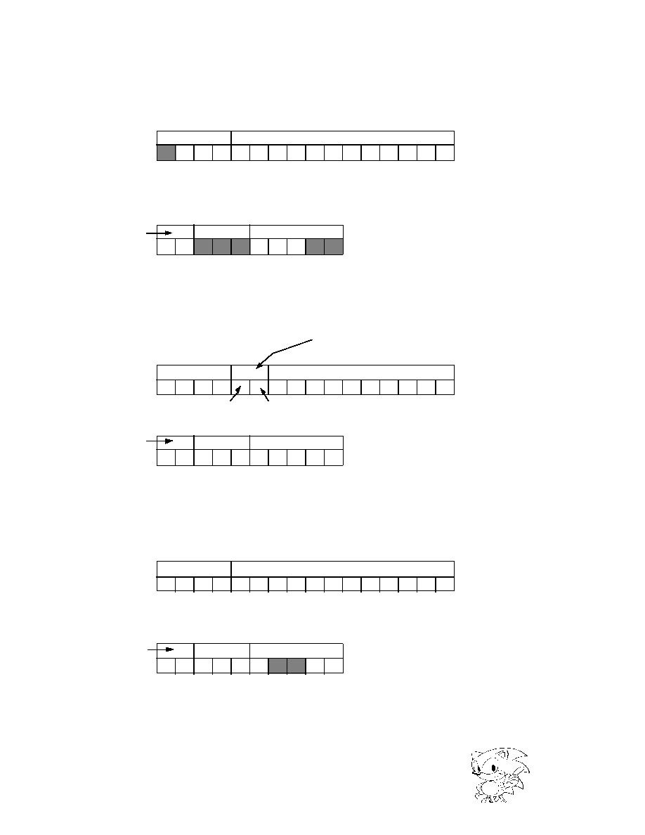
SEGA Confidential
(4 ) Cha ra ct er Size : 1 H ce ll X 1 V ce ll
Cha ra ct er Colo r Coun t : Exce pt 16 col or s
Bit 15
8
7
6
5
4
3
2
1
0
9
10
11
12
13
14
Pal et te Numb er
Cha ra ct er Numb er
6
5
4
3
2
1
0
4
5
6
7
8
9
Pattern Nam e Da ta in Pat tern Name Tab le
Bit 9
8
7
6
5
4
3
2
1
0
Pal et te No.
Cha ra ct er Num ber
PR
CC
12
13
14
10
11
(5 ) Cha ra ct er Size : 2 H ce ll s X 2 V ce ll s
Cha ra ct er Colo r Coun t : 16 Col or s
Bit 15
8
7
6
5
4
3
2
1
0
9
10
11
12
13
14
Pal et te Numb er
Cha ra ct er Numb er
3
2
1
0
5
4
3
2
6
7
8
9
10
11
Pattern Nam e Da ta in Pat tern Name Tab le
Bit 9
8
7
6
5
4
3
2
1
0
Pal et te No.
Cha ra ct er Num ber
PR
CC
6
5
0
1
12
13
14
4
(6 ) Cha ra ct er Size : 2 H ce ll s X 2 V ce ll s
Cha ra ct er Colo r Coun t : 16 Col or s
Bit 15
8
7
6
5
4
3
2
1
0
9
10
11
12
13
14
Pal et te Numb er
Char act er Nu mber
3
2
1
0
3
2
4
5
6
7
8
11
Pattern Nam e Da ta in Pat tern Name Tab le
Bit 9
8
7
6
5
4
3
2
1
0
Pal et te No.
Cha ra ct er Num ber
PR
CC
6
5
14
4
12
13
10
9
0
1
Speci al
Fun ct ion
Speci al
Fun ct ion
Spe cia l
Funct ion
PR : Speci al Pri orit y Bi t
CC: Sp ecia l C ol or Calcu lat ion Bi t
PR : Speci al Pri orit y Bi t
CC: Sp ecia l C ol or Calcu lat ion Bi t
Cha ra ct er Num ber Supp le me nt Mo de : Mod e 1
Not e: Bot h ver tica l and hor izo nt al flip fun ct ion bi ts are se t to 0.
Shad ed bi t is ig no re d
Suppl eme nt al Dat a in Pat t er n Na me Con trol Reg ist er
PR: Sp ecia l Pr io ri ty Bit
CC: Spec ial Colo r Calc ul atio n Bit
No te: Shad ed bi ts ar e igno re d
Cha ra ct er Num ber Supp le me nt Mo de : Mod e 0
Flip Fun ct ion
Vert ica l
Ho ri zo nt al
Supp le me nt al Dat a in Pat ter n Na me Con trol Reg ist er
Cha ract er Nu mb er Supp lem en t Mod e: Mo de 1
Not e: Bot h ve rt ica l an d hor izon tal f li p fun ct ion bi ts ar e set t o 0.
Sup pl em ent al Da ta in Pat t er n Name Con tro l Reg ist er
No te: Shad ed bi ts ar e igno re d
Figure 4.10 Configuration when pattern name data is one word (continued)
72
|

SEGA Confidential
(7 ) Cha ra ct er Size : 2 H ce ll s X 2 V ce ll s
Cha ract er Co lor Cou nt : Exce pt 16 col or s
Bit 15
8
7
6
5
4
3
2
1
0
9
10
11
12
13
14
Palet te Num be r
Cha ra ct er Nu mb er
6
5
4
3
2
4
5
6
7
8
9
Pattern Nam e Da ta in Pattern Nam e Tabl e
Bit 9
8
7
6
5
4
3
2
1
0
Pal et t e No.
Cha ra ct er Nu mb er
PR
CC
12
13
14
0
1
10
11
(8 ) Cha ra ct er Size : 2 H ce ll s X 2 V ce ll s
Cha ract er Co lor Cou nt : Exce pt 16 col or s
Bit 15
8
7
6
5
4
3
2
1
0
9
10
11
12
13
14
Palet t e Numb er
Cha ra ct er Nu mb er
6
5
4
3
2
4
5
6
7
8
9
Pattern Nam e Da ta in Pattern Nam e Tabl e
Bit 9
8
7
6
5
4
3
2
1
0
Pal et t e No.
Char act er Num be r
PR
CC
14
10
11
12
13
0
1
Cha ract er Nu mb er Supp lem en t Mod e: Mo de 0
Suppl eme nt al Dat a in Pat ter n Na me Con trol Reg ist er
Note: Shad ed bi t is ig no re d
Flip Funct ion
Ver tical
Hor izo nt al
Speci al
Fun ct ion
PR: Sp ecia l Pr io ri ty Bit
CC: Spec ial Colo r Calc ula tio n Bit
Not e: Sha ded bit s ar e ig no re d
Cha ract er Nu mb er Supp lem en t Mod e: Mo de 1
Not e: Bot h ve rt ica l an d hor izon tal f li p fun ct ion bi ts ar e se t t o 0.
Sha de d bit is ign or ed
Suppl eme nt al Dat a in Pat ter n Na me Con trol Reg ist er
Speci al
Fun ct ion
PR: Sp ecia l Pr io ri ty Bit
CC: Spec ial Colo r Calc ula tio n Bit
Not e: Shade d bi ts are ign or ed
Figure 4.10 Configuration when pattern name data is one word (continued)
ST-58-R2
73
|

SEGA Confidential
Character Number
The character number is 15-bit data, and designates the address of the character
pattern being displayed in that position. The boundary of the character pattern from
this character number is always 20H. Moreover, when the VRAM size is 4M bits, the
most significant bit of the character number (bit 14) is not used.
Palette Number
The palette number is 7-bit data, and designates the address of the color palette used
in the character pattern being displayed in that position. This data can be used only
when the color format is the palette format, not the RGB format. The palette number
is added to the dot color code of the character pattern. Because there is a total of 11
bits of dot color data, the bits that are used change depending on the character color
number. Figure 4.11 shows the configuration of 11-bit dot color data.
Pal ette Nu mbe r
3
2
1
0
4
5
6
3
2
1
0
Dot Col or Cod e
Cha ra ct er Colo r Co un t : 16 Col or s
Pal ette No .
7
6
5
4
4
5
6
3
2
1
0
Dot Col or Code
Cha ra ct er Colo r Coun t : 25 6 Colo rs
7
6
5
4
8
9
10
3
2
1
0
Do t Colo r Co de
Cha ra ct er Colo r Coun t : 20 48 Col or s
Figure 4.11 Dot color data by character color number
Special Function Bit
The special function bit is 2-bit data, and designates whether to use the special
function for the character pattern being displayed at that position. The special
function bit has a special priority bit that controls the priority number, and a special
color calculation bit that controls color operation. See "11.2 Special Priority Func-
tion" for more about the special priority bit, and "12.3 Special Color Calculation
Function" for more about the special color calculation bit.
74
|

SEGA Confidential
Reverse (Flip) Function Bit
The reverse function bit is 2-bit data, and designates whether to use the reverse
function for the character pattern being displayed at that position. The reverse
function bit has a top-bottom reverse bit that reverses the top and bottom of a char-
acter pattern, and a left-right reverse bit that reverses left and right. The reverse
function bit is shown in Table 4.7, and a reverse display of a character pattern in
shown in Figure 4.12.
Table 4.7 Reverse Function Bit
Figure 4.12 Reverse display of character patterns
Vertical Flip Bit
Horizontal Flip Bit
Process
0
0
Cannot flip vertically or horizontally
0
1
Horizontal flipping only
1
0
Vertical flipping only
1
1
Can flip both vertically and horizontally
Ver tical Flip Bit =0
Hor izon tal Flip Bit =0
Hori z. Flip
Ve rt. Flip
Hori z. and Ver t. Fli p
Ver tica l Fl ip Bit =1
Hor izon tal Flip Bit =0
Vert ica l Fli p Bit =1
Hori zon tal Fl ip Bit =1
Ver tical Flip Bit =0
Hor izo nt al Flip Bit =1
ST-58-R2
75
|

SEGA Confidential
Pattern Name Control Register
The pattern name control register assigns pattern name data size, character number
supplement mode, and pattern name supplement data. This register is a write only
16-bit register located in addresses 180030H to 180038H. Because the value of the
register is cleared to 0 after the power is turned on or reset, the value must be set.
Pattern name data size bit (N0PNB, N1PNB, N2PNB, N3PNB, R0PNB)
Designates the pattern name data size when displaying in the cell format.
15
14
13
12
11
10
9
8
PNCN0
N0PNB
N0CNSM
~
~
~
~
N0SPR
N0SCC
180030H
7
6
5
4
3
2
1
0
N0SPLT6 N0SPLT5 N0SPLT4
N0SCN4
N0SCN3
N0SCN2
N0SCN1
N0SCN0
15
14
13
12
11
10
9
8
PNCN1
N1PNB
N1CNSM
~
~
~
~
N1SPR
N1SCC
180032H
7
6
5
4
3
2
1
0
N1SPLT6 N1SPLT5 N1SPLT4
N1SCN4
N1SCN3
N1SCN2
N1SCN1
N1SCN0
15
14
13
12
11
10
9
8
PNCN2
N2PNB
N2CNSM
~
~
~
~
N2SPR
N2SCC
180034H
7
6
5
4
3
2
1
0
N2SPLT6 N2SPLT5 N2SPLT4
N2SCN4
N2SCN3
N2SCN2
N2SCN1
N2SCN0
15
14
13
12
11
10
9
8
PNCN3
N3PNB
N3CNSM
~
~
~
~
N3SPR
N3SCC
180036H
7
6
5
4
3
2
1
0
N3SPLT6 N3SPLT5 N3SPLT4
N3SCN4
N3SCN3
N3SCN2
N3SCN1
N3SCN0
15
14
13
12
11
10
9
8
PNCR
R0PNB
R0CNSM
~
~
~
~
R0SPR
R0SCC
180038H
7
6
5
4
3
2
1
0
R0SPLT6 R0SPLT5 R0SPLT4
R0SCN4
R0SCN3
R0SCN2
R0SCN1
R0SCN0
N0PNB
180030H
Bit 15
For NBG0 (or RBG 1)
N1PNB
180032H
Bit 15
For NBG1
N2PNB
180034H
Bit 15
For NBG2
N3PNB
180036H
Bit 15
For NBG3
R0PNB
180038H
Bit 15
For RBG0
76
|

SEGA Confidential
Note: N0, N1, N3, or R0 is entered in bit name for xx.
Character number supplement bit (N0CNSM, N1CNSM, N2CNSM, N3CNSM, R0CNSM)
Designates the character number supplement mode when the pattern name data size
in the pattern name table is 1-word.
Note: N0, N1, N2, N3, or R0 is entered in bit name for xx.
Special priority bit (for pattern name supplement data): Supplementary special priority bit
(N0SPR, N1SPR, N2SPR, N3SPR, R0SPR)
Designates the pattern name supplement data as the special priority bit when the
pattern name data size is 1-word.
See "11.2 Special Color Priority Function" for how this bit is used.
N0CNSM
180030H
Bit 14
For NBG0 (or RBG 1)
N1CNSM
180032H
Bit 14
For NBG1
N2CNSM
180034H
Bit 14
For NBG2
N3CNSM
180036H
Bit 14
For NBG3
R0CNSM
180038H
Bit 14
For RBG0
x x C N S M
Character Number
Auxiliary Mode
Process
0
0
Character number in pattern name data is 10 bits.
Flip function can be selected in character units.
1
1
Character number in pattern name data is 12 bits.
Flip function cannot be used.
N0SPR
180030H
Bit 9
For NBG0 (or RBG 1)
N1SPR
180032H
Bit 9
For NBG1
N2SPR
180034H
Bit 9
For NBG2
N3SPR
180036H
Bit 9
For NBG3
R0SPR
180038H
Bit 9
For RBG0
ST-58-R2
77
xxPNB
Pattern Name Data Size
0
2 Words
1
1 Word
|

SEGA Confidential
Special color calculation bit (for pattern name supplement data): Supplementary special color
calculation bit (N0SCC, N1SCC, N2SCC, N3SCC, R0SCC)
The special color calculation bit is designated as pattern name supplement data
when the pattern name data size is 1-word.
See "12.2 Special Color Calculation Function" to learn how this bit is used.
Supplementary palette number bit (N0SPLT6 to N0SPLT4, N1SPLT6 to N1SPLT4, N2SPLT6 to
N2SPLT4, N3SPLT6 to N3SPLT4, R0SPLT6 to R0SPLT4)
Designates the palette number bit as pattern name supplement data when the pat-
tern name data size is 1-word. Three bits are added to the palette number bit of the
pattern name data for the supplementary palette number bit.
Supplementary character number bit (N0SCN4 to N0SCN0, N1SCN4 to N1SCN0, N2SCN4 to
N2SCN0, N3SCN4 to N3SCN0, R0SCN4 to R0SCN0)
Designates the character number bit as the pattern name supplement data when the
pattern name data size is 1-word. Five bits are added to the palette number bit of
the pattern name data for the supplementary palette number bit.
N0SCC
180030H
Bit 8
For NBG0 (or RBG 1)
N1SCC
180032H
Bit 8
For NBG1
N2SCC
180034H
Bit 8
For NBG2
N3SCC
180036H
Bit 8
For NBG3
R0SCC
180038H
Bit 8
For RBG0
N0SPLT6~N0SPLT4
180030H
Bit 7~5
For NBG0 (or RBG 1)
N1SPLT6~N1SPLT4
180032H
Bit 7~5
For NBG1
N2SPLT6~N2SPLT4
180034H
Bit 7~5
For NBG2
N3SPLT6~N3SPLT4
180036H
Bit 7~5
For NBG3
R0SPLT6~R0SPLT4
180038H
Bit 7~5
For RBG0
N0SCN4~N0SCN0
180030H
Bit 4~0
For NBG0 (or RBG 1)
N1SCN4~N1SCN0
180032H
Bit 4~0
For NBG1
N2SCN4~N2SCN0
180034H
Bit 4~0
For NBG2
N3SCN4~N3SCN0
180036H
Bit 4~0
For NBG3
R0SCN4~R0SCN0
180038H
Bit 4~0
For RBG0
78
|

SEGA Confidential
4.7 Planes
Plane arranges the pattern name table (page) in sizes of 1 x 1, 2 x 1, or 2 x 2. Size is
designated in its respective register.
Plane Size
When the plane consists of more than one pattern name table (page), the pattern
name table used by one plane should be linked to VRAM and stored. Figure 4.13
shows the relationship of the pattern name table arranged by plane size (number of
plane page) and pattern name table.
Whe n 1 H page X 1 V pa ge
Pag e 0
Pag e 1
Pag e 2
Pag e 3
64 Cel ls
64 Cel ls
12 8 Cel ls
12 8 Cel ls
Pag e 0
Pag e 1
Pag e 2
Pag e 3
Select ed
Pattern Nam e
Tab le Heade r
Addr ess
Pat ter n Na me Tab le
Pag e 4
Pag e 1
64 Ce lls
12 8 Cel ls
Pag e 0
Whe n 2 H pa ge s X 1 V pa ge
Wh en 2 H pag es X 2 V page s
Page 0
Figure 4.13 Arrangement of pattern name table by plane size
ST-58-R2
79
|

SEGA Confidential
Plane Size Register
The plane size register controls the plane size and setting of the screen-over process
of the rotation scroll surface. This register is a write only 16-bit register located at
address 18003AH. Because the value of the register is cleared to 0 after the power is
turned on or reset, the value must be set.
Plane size bit (N0PLSZ1, N0PLSZ0, N1PLSZ1, N1PLSZ0, N2PLSZ1, N2PLSZ0, N3PLSZ1,
N3PLSZ0, RAPLSZ1, RAPLSZ0, RBPLSZ1, RBPLSZ0
)
Designates the plane size (number of pages) of each scroll screen.
Note: N0, N1, N2, N3, RA, or RB is entered in bit name for xx.
When the reduction display is set up to a factor of 1/4 in NBG0 and NBG1, do not
set the plane size of that screen to 2 H pages x 2 V pages.
15
14
13
12
11
10
9
8
PLSZ
RBOVR1
RBOVR0
RBPLSZ1 RBPLSZ0
RAOVR1
RAOVR0
RAPLSZ1 RAPLSZ0
18003AH
7
6
5
4
3
2
1
0
N3PLSZ1 N3PLSZ0 N2PLSZ1 N2PLSZ0 N1PLSZ1 N1PLSZ0 N0PLSZ1 N0PLSZ0
N0PLSZ1, N0PLSZ0
18003AH
Bit 1,0
For NBG0
N1PLSZ1, N1PLSZ0
18003AH
Bit 3,2
For NBG1
N2PLSZ1, N2PLSZ0
18003AH
Bit 5,4
For NBG2
N3PLSZ1, N3PLSZ0
18003AH
Bit 7,6
For NBG3
RAPLSZ1, RAPLSZ0
18003AH
Bit 9,8
For Rotation Parameter A
RBPLSZ1, RBPLSZ0
18003AH
Bit 13,12
For Rotation Parameter B
xxPLSZ1
xxPLSZ0
Plane Size
0
0
1 H Page X 1 V Page
0
1
2 H Pages X 1 V Page
1
0
Invalid (Do not set.)
1
1
2 H Pages X 2 V Pages
80
|

SEGA Confidential
Screen-over process bit: Over bit (RAOVR1, RAOVR0, RBOVR1, RBOVR0)
Designates control (screen-over process) when the display coordinate value exceeds
the display area in the rotation scroll surface.
Note: A or B is entered in bit name for x.
When the rotation scroll surface is in bit map, the character pattern designated by
the screen-over pattern name register must not be set to repeat process. With the
rotation scroll surface in bit map, and when the length of the bit map is 256 dots, if
the display area is set to 0
X < 512 and 0
Y < 512 and all the outer area is set to be
transparent, two of the same images will be displayed for each 256 V dots.
RAOVR1, RAOVR0
18003AH
Bit 11,10
For Rotation Parameter A
RBOVR1, RBOVR0
18003AH
Bit 15,14
For Rotation Parameter B
RxOVR1
RxOVR0
Screen Over Process
0
0
Outside the display area, the image set in the display area is repeated
0
1
Outside the display area, the character pattern specified by screen ove
pattern name register is repeated. (Only when the rotation scroll
surface is in cell format.)
1
0
Outside the display area, the scroll screen is transparent,
1
1
Set the display area as 0
X
512, 0
Y
512 regardless of plane size or
bitmap size and make that area transparent.
ST-58-R2
81
|

SEGA Confidential
4.8
Maps
Maps are square patterns consisting of 2 x 2 or 4 x 4 planes. A map of a Normal
scroll screen consists of a 2 x 2 plane, and a map of a rotation scroll surface consists
of a 4 x 4 plane. The method of arranging the plane is made by selecting the pattern
name table lead address in various plane registers.
Map Selection Register
Maps are organized into four planes (normal scroll screen) or 16 planes (rotation
scroll surface). Each screen has for each plane number a 6-bit map register to select
the pattern name table lead address for various planes. It also has a map offset
register of three bits added to the highest map register. The total 9-bit map selection
register changes the bit used and the register displaying the address value, depend-
ing on the pattern name data size and character size. Figure 4.14 shows the relation-
ship of the map register and map offset register.
Map Reg ist er A
3
2
1
0
4
5
Map Offse t Reg ist er
8
7
6
Ma p Re gi st er B
3
2
1
0
4
5
2
1
0
Ma p Re gi st er
3
4
5
6
7
8
Map Offse t Regi st er
Figure 4.14 Map selection register
Table 4.8 shows the address values of register and bits that are used for the map
selection register by the pattern name data size and character size.
82
|

SEGA Confidential
Table 4.8 Address value of map designated register by setting
Note: When the VRAM capacity is set at 4M bits, the most significant bit among the bits used is not
used.
Plane Size
Pattern Name
Data Size
Character Size
Bits and Addresses
1 Word
1 H Cell X 1 V Cell
(Value of bit 6~0) X 2000H
1 H page X
2 H Cells X 2 V Cells
(Value of bit 8~0) X 800H
1 V page
2 Words
1 H Cell X 1 V Cell
(Value of bit 5~0) X 4000H
2 H Cells X 2 V Cells
(Value of bit 7~0) X 1000H
1 Word
1 H Cell X 1 V Cell
(Value of bit 6~1) X 4000H
2 H pages X
2 H Cells X 2 V Cells
(Value of bit 8~1) X 1000H
1 V page
2 Words
1 H Cell X 1 V Cell
(Value of bit 5~1) X 8000H
2 H Cells X 2 V Cells
(Value of bit 7~1) X 2000H
1 Word
1 H Cell X 1 V Cell
(Value of bit 6~2) X 8000H
2 H pages X
2 V Cells X 2 V Cells
(Value of bit 8~2) X 2000H
2 V pages
2 Words
1 H Cell X 1 V Cell
(Value of bit 5~2) X 10000H
2 H Cells X 2 V Cells
(Value of bit 7~2) X 4000H
ST-58-R2
83
|

SEGA Confidential
Map Size
Map size (number of planes in the map) will change depending on if the screen is a
normal scroll screen or rotation scroll surface. The normal scroll screen has a map 2
H planes X 2 V planes in each screen. The rotation scroll surface has a map 4 H
planes X 4 V planes in both of rotation parameters A and B. Figure 4.15 shows the
plane arrangements of different map sizes.
Plane
A
Normal Scroll Screen
Rotation Scroll Screen
Plane
B
Plane
C
Plane
D
Plane
A
Plane
B
Plane
E
Plane
F
Plane
C
Plane
D
Plane
G
Plane
H
Plane
I
Plane
J
Plane
M
Plane
N
Plane
K
Plane
L
Plane
O
Plane
P
Figure 4.15 Map size
84
|

SEGA Confidential
When NBG0 and NBG1 enable bits (N0ZMQT and N1ZMQT) are set to allow reduc-
tion up to a factor of 1/4, the map size of NBG0 and NBG1 become normal. A set
screen plane size, that can be reduced up to 1/4 should not be 2 H pages X 2 V
pages. Figure 4.16 shows the map size by the reduction setting.
When se tting NBG0, ca n
be red uce d up t o 1/4.
Plan e A
For NB G0
Plan e B
Fo r NBG0
Pla ne D
For NBG 0
Plane C
For NBG0
Plan e A
For NB G2
Plan e B
Fo r NBG2
Pla ne D
For NBG 2
Plane C
For NBG2
Plane A
For NBG1
Plane B
For NBG1
Plane D
For NBG1
Plan e C
For NB G1
Plane A
For NBG3
Plane B
For NBG3
Plane D
For NBG3
Plan e C
For NB G3
Whe n se tting NBG1, ca n
be red uce d up t o 1/4.
Figure 4.16 Plane arrangement of map by reduction settings
Map Offset Register
The map offset register designates the map offset value. This is a write-only 16-bit
register, with addresses located at 18003CH to 18003EH. Because the value of the
register is cleared to 0 after the power is turned on or reset, the value must be set.
15
14
13
12
11
10
9
8
MPOFN
~
N3MP8
N3MP7
N3MP6
~
N2MP8
N2MP7
N2MP6
18003CH
7
6
5
4
3
2
1
0
~
N1MP8
N1MP7
N1MP6
~
N0MP8
N0MP7
N0MP6
15
14
13
12
11
10
9
8
MPOFR
~
~
~
~
~
~
~
~
18003EH
7
6
5
4
3
2
1
0
~
RBMP8
RBMP7
RBMP6
~
RAMP8
RAMP7
RAMP6
ST-58-R2
85
|

SEGA Confidential
Map offset bit (N0MP8 to N0MP6, N1MP8 to N1MP6, N2MP8 to N2MP6, N3MP8 to N3MP6,
RAMP8 to RAMP6, RBMP8 to RBMP6)
When the scroll screen display format is the cell format, the map offset value of 3 bits
is added to the highest 6 bits of the map register. This designates the bit map pattern
boundary when in the bit map format.
Boundary address of the bit map pattern is shown below:
(boundary address value of the bit map pattern) = (map offset register value 3 bit) x
20000H.
N0MP8~N0MP6
18003CH
Bit 2~0
For NBG0
N1MP8~N1MP6
18003CH
Bit 6~4
For NBG1
N2MP8~N2MP6
18003CH
Bit 10~8
For NBG2
N3MP8~N3MP6
18003CH
Bit 14~12
For NBG3
RAMP8~RAMP6
18003EH
Bit 2~0
For Rotation Parameter A
RBMP8~RBMP6
18003EH
Bit 6~4
For Rotation Parameter B
86
|

SEGA Confidential
Normal Scroll Screen Map Register
Normal scroll screen map register designates the lead address of the pattern name
table of each plane when the normal scroll screen is displayed in the cell format.
This register is a write-only 16-bit register, with addresses located at 180040H to
18004EH. Because the value of the register is cleared to 0 after the power is turned
on or reset, the value must be set.
15
14
13
12
11
10
9
8
MPABN0
~
~
N0MPB5
N0MPB4
N0MPB3
N0MPB2
N0MPB1
N0MPB0
180040H
7
6
5
4
3
2
1
0
~
~
N0MPA5
N0MPA4
N0MPA3
N0MPA2
N0MPA1
N0MPA0
15
14
13
12
11
10
9
8
MPCDN0
~
~
N0MPD5
N0MPD4
N0MPD3
N0MPD2
N0MPD1
N0MPD0
180042H
7
6
5
4
3
2
1
0
~
~
N0MPC5
N0MPC4
N0MPC3
N0MPC2
N0MPC1
N0MPC0
15
14
13
12
11
10
9
8
MPABN1
~
~
N1MPB5
N1MPB4
N1MPB3
N1MPB2
N1MPB1
N1MPB0
180044H
7
6
5
4
3
2
1
0
~
~
N1MPA5
N1MPA4
N1MPA3
N1MPA2
N1MPA1
N1MPA0
15
14
13
12
11
10
9
8
MPCDN1
~
~
N1MPD5
N1MPD4
N1MPD3
N1MPD2
N1MPD1
N1MPD0
180046H
7
6
5
4
3
2
1
0
~
~
N1MPC5
N1MPC4
N1MPC3
N1MPC2
N1MPC1
N1MPC0
15
14
13
12
11
10
9
8
MPABN2
~
~
N2MPB5
N2MPB4
N2MPB3
N2MPB2
N2MPB1
N2MPB0
180048H
7
6
5
4
3
2
1
0
~
~
N2MPA5
N2MPA4
N2MPA3
N2MPA2
N2MPA1
N2MPA0
15
14
13
12
11
10
9
8
MPCDN2
~
~
N2MPD5
N2MPD4
N2MPD3
N2MPD2
N2MPD1
N2MPD0
18004AH
7
6
5
4
3
2
1
0
~
~
N2MPC5
N2MPC4
N2MPC3
N2MPC2
N2MPC1
N2MPC0
15
14
13
12
11
10
9
8
MPABN3
~
~
N3MPB5
N3MPB4
N3MPB3
N3MPB2
N3MPB1
N3MPB0
18004CH
7
6
5
4
3
2
1
0
~
~
N3MPA5
N3MPA4
N3MPA3
N3MPA2
N3MPA1
N3MPA0
15
14
13
12
11
10
9
8
MPCDN3
~
~
N3MPD5
N3MPD4
N3MPD3
N3MPD2
N3MPD1
N3MPD0
18004EH
7
6
5
4
3
2
1
0
~
~
N3MPC5
N3MPC4
N3MPC3
N3MPC2
N3MPC1
N3MPC0
ST-58-R2
87
|
SEGA Confidential
Map bit (for normal scroll): (N0MPA5 to N0MPA0, N0MPB5 to N0MPB0,
N0MPC5 to N0MPC0, N0MPD5 to N0MPD0, N1MPA5 to N1MPA0, N1MPB5 to N1MPB0, N1MPC5
to N1MPC0, N1MPD5 to N1MPD0, N2MPA5 to N2MPA0, N2MPB5 to N2MPB0, N2MPC5 to
N2MPC0, N2MPD5 to N2MPD0, N3MPA5 to N3MPA0, N3MPB5 to N3MPB0, N3MPC5 to N3MPC0,
N3MPD5 to N3MPD0)
The lead address for the pattern name table is designated for each plane, when the
Normal scroll screen is displayed by the cell format.
N0MPA5~N0MPA0
180040H
Bit 5~0
For NBG0 Plane A
N0MPB5~N0MPB0
180040H
Bit 13~8
For NBG0 Plane B
N0MPC5~N0MPC0
180042H
Bit 5~0
For NBG0 Plane C
N0MPD5~N0MPD0
180042H
Bit 13~8
For NBG0 Plane D
N1MPA5~N1MPA0
180044H
Bit 5~0
For NBG1 Plane A
N1MPB5~N1MPB0
180044H
Bit 13~8
For NBG1 Plane B
N1MPC5~N1MPC0
180046H
Bit 5~0
For NBG1 Plane C
N1MPD5~N1MPD0
180046H
Bit 13~8
For NBG1 Plane D
N2MPA5~N2MPA0
180048H
Bit 5~0
For NBG2 Plane A
N2MPB5~N2MPB0
180048H
Bit 13~8
For NBG2 Plane B
N2MPC5~N2MPC0
18004AH
Bit 5~0
For NBG2 Plane C
N2MPD5~N2MPD0
18004AH
Bit 13~8
For NBG2 Plane D
N3MPA5~N3MPA0
18004CH
Bit 5~0
For NBG3 Plane A
N3MPB5~N3MPB0
18004CH
Bit 13~8
For NBG3 Plane B
N3MPC5~N3MPC0
18004EH
Bit 5~0
For NBG3 Plane C
N3MPD5~N3MPD0
18004EH
Bit 13~8
For NBG3 Plane D
88
|

SEGA Confidential
Rotation Scroll Surface Map Register
The Rotation Scroll Surface Map Register designates the lead address of the pattern
name table arranged in each plane by rotation parameters A and B. When a write-
only 16-bit register, with addresses located at 180050H to 18006EH. Because the
value of the register is cleared to 0 after the power is turned on or reset, the value
must be set.
15
14
13
12
11
10
9
8
MPABRA
~
~
RAMPB5
RAMPB4
RAMPB3
RAMPB2
RAMPB1
RAMPB0
180050H
7
6
5
4
3
2
1
0
~
~
RAMPA5
RAMPA4
RAMPA3
RAMPA2
RAMPA1
RAMPA0
15
14
13
12
11
10
9
8
MPCDRA
~
~
RAMPD5
RAMPD4
RAMPD3
RAMPD2
RAMPD1
RAMPD0
180052H
7
6
5
4
3
2
1
0
~
~
RAMPC5
RAMPC4
RAMPC3
RAMPC2
RAMPC1
RAMPC0
15
14
13
12
11
10
9
8
MPEFRA
~
~
RAMPF5
RAMPF4
RAMPF3
RAMPF2
RAMPF1
RAMPF0
180054H
7
6
5
4
3
2
1
0
~
~
RAMPE5
RAMPE4
RAMPE3
RAMPE2
RAMPE1
RAMPE0
15
14
13
12
11
10
9
8
MPGHRA
~
~
RAMPH5
RAMPH4
RAMPH3
RAMPH2
RAMPH1
RAMPH0
180056H
7
6
5
4
3
2
1
0
~
~
RAMPG5
RAMPG4
RAMPG3
RAMPG2
RAMPG1
RAMPG0
15
14
13
12
11
10
9
8
MPIJRA
~
~
RAMPJ5
RAMPJ4
RAMPJ3
RAMPJ2
RAMPJ1
RAMPJ0
180058H
7
6
5
4
3
2
1
0
~
~
RAMPI5
RAMPI4
RAMPI3
RAMPI2
RAMPI1
RAMPI0
15
14
13
12
11
10
9
8
MPKLRA
~
~
RAMPL5
RAMPL4
RAMPL3
RAMPL2
RAMPL1
RAMPL0
18005AH
7
6
5
4
3
2
1
0
~
~
RAMPK5
RAMPK4
RAMPK3
RAMPK2
RAMPK1
RAMPK0
15
14
13
12
11
10
9
8
MPMNRA
~
~
RAMPN5
RAMPN4
RAMPN3
RAMPN2
RAMPN1
RAMPN0
18005CH
7
6
5
4
3
2
1
0
~
~
RAMPM5 RAMPM4 RAMPM3 RAMPM2 RAMPM1 RAMPM0
15
14
13
12
11
10
9
8
MPOPRA
~
~
RAMPP5
RAMPP4
RAMPP3
RAMPP2
RAMPP1
RAMPP0
18005EH
7
6
5
4
3
2
1
0
~
~
RAMPO5
RAMPO4
RAMPO3
RAMPO2
RAMPO1
RAMPO0
ST-58-R2
89
|

SEGA Confidential
15
14
13
12
11
10
9
8
MPABRB
~
~
RBMPB5
RBMPB4
RBMPB3
RBMPB2
RBMPB1
RBMPB0
180060H
7
6
5
4
3
2
1
0
~
~
RBMPA5
RBMPA4
RBMPA3
RBMPA2
RBMPA1
RBMPA0
15
14
13
12
11
10
9
8
MPCDRB
~
~
RBMPD5
RBMPD4
RBMPD3
RBMPD2
RBMPD1
RBMPD0
180062H
7
6
5
4
3
2
1
0
~
~
RBMPC5
RBMPC4
RBMPC3
RBMPC2
RBMPC1
RBMPC0
15
14
13
12
11
10
9
8
MPEFRB
~
~
RBMPF5
RBMPF4
RBMPF3
RBMPF2
RBMPF1
RBMPF0
180064H
7
6
5
4
3
2
1
0
~
~
RBMPE5
RBMPE4
RBMPE3
RBMPE2
RBMPE1
RBMPE0
15
14
13
12
11
10
9
8
MPGHRB
~
~
RBMPH5
RBMPH4
RBMPH3
RBMPH2
RBMPH1
RBMPH0
180066H
7
6
5
4
3
2
1
0
~
~
RBMPG5
RBMPG4
RBMPG3
RBMPG2
RBMPG1
RBMPG0
15
14
13
12
11
10
9
8
MPIJRB
~
~
RBMPJ5
RBMPJ4
RBMPJ3
RBMPJ2
RBMPJ1
RBMPJ0
180068H
7
6
5
4
3
2
1
0
~
~
RBMPI5
RBMPI4
RBMPI3
RBMPI2
RBMPI1
RBMPI0
15
14
13
12
11
10
9
8
MPKLRB
~
~
RBMPL5
RBMPL4
RBMPL3
RBMPL2
RBMPL1
RBMPL0
18006AH
7
6
5
4
3
2
1
0
~
~
RBMPK5
RBMPK4
RBMPK3
RBMPK2
RBMPK1
RBMPK0
15
14
13
12
11
10
9
8
MPMNRB
~
~
RBMPN5
RBMPN4
RBMPN3
RBMPN2
RBMPN1
RBMPN0
18006CH
7
6
5
4
3
2
1
0
~
~
RBMPM5 RBMPM4 RBMPM3 RBMPM2 RBMPM1 RBMPM0
15
14
13
12
11
10
9
8
MPOPRB
~
~
RBMPP5
RBMPP4
RBMPP3
RBMPP2
RBMPP1
RBMPP0
18006EH
7
6
5
4
3
2
1
0
~
~
RBMPO5
RBMPO4
RBMPO3
RBMPO2
RBMPO1
RBMPO0
90
|

SEGA Confidential
Map bit (for rotation scroll): Map bit (RAMPA5 to RAMPA0, RAMPB5 to RAMPB0,
RAMPC5 to RAMPC0, RAMPD5 to RAMPD0, RAMPE5 to RAMPE0,
RAMPF5 to RAMPF0, RAMPG5 to RAMPG0, RAMPH5 to RAMPH0,
RAMPI5 to RAMPI0, RAMPJ5 to RAMPJ0, RAMPK5 to RAMPK0,
RAMPL5 to RAMPL0, RAMPM5 to RAMPM0, RAMPN5 to RAMPN0,
RAMPO5 to RAMPO0, RAMPP5 to RAMPP0, RBMPA5 to RBMPA0,
RBMPB5 to RBMPB0, RBMPC5 to RBMPC0, RBMPD5 to RBMPD0,
RBMPE5 to RBMPE0, RBMPF5 to RBMPF0, RBMPG5 to RBMPG0,
RBMPH5 to RBMPH0, RAMPI5 to RBMPI0, RBMPJ5 to RBMPJ0,
RBMPK5 to RBMPK0, RBMPL5 to RBMPL0, RBMPM5 to RBMPM0,
RBMPN5 to RBMPN0, RBMPO5 to RBMPO0, RBMPP5 to RBMPP0)
When a rotation scroll surface is displayed in the cell format, it designates the lead
address of the pattern name table being arranged in each plane .
ST-58-R2
91
|

SEGA Confidential
RAMPA5~RAMPA0
180050H
Bit 5~0
Rotation Parameter A for Screen Plane A
RAMPB5~RAMPB0
180050H
Bit 13~8
Rotation Parameter A for Screen Plane B
RAMPC5~RAMPC0
180052H
Bit 5~0
Rotation Parameter A for Screen Plane C
RAMPD5~RAMPD0
180052H
Bit 13~8
Rotation Parameter A for Screen Plane D
RAMPE5~RAMPE0
180054H
Bit 5~0
Rotation Parameter A for Screen Plane E
RAMPF5~RAMPF0
180054H
Bit 13~8
Rotation Parameter A for Screen Plane F
RAMPG5~RAMPG0
180056H
Bit 5~0
Rotation Parameter A for Screen Plane G
RAMPH5~RAMPH0
180056H
Bit 13~8
Rotation Parameter A for Screen Plane H
RAMPI5~RAMPI0
180058H
Bit 5~0
Rotation Parameter A for Screen Plane I
RAMPJ5~RAMPJ0
180058H
Bit 13~8
Rotation Parameter A for Screen Plane J
RAMPK5~RAMPK0
18005AH
Bit 5~0
Rotation Parameter A for Screen Plane K
RAMPL5~RAMPL0
18005AH
Bit 13~8
Rotation Parameter A for Screen Plane L
RAMPM5~RAMPM0
18005CH
Bit 5~0
Rotation Parameter A for Screen Plane M
RAMPN5~RAMPN0
18005CH
Bit 13~8
Rotation Parameter A for Screen Plane N
RAMPO5~RAMPO0
18005EH
Bit 5~0
Rotation Parameter A for Screen Plane O
RAMPP5~RAMPP0
18005EH
Bit 13~8
Rotation Parameter A for Screen Plane P
RBMPA5~RBMPA0
180060H
Bit 5~0
Rotation Parameter B for Screen Plane A
RBMPB5~RBMPB0
180060H
Bit 13~8
Rotation Parameter B for Screen Plane B
RBMPC5~RBMPC0
180062H
Bit 5~0
Rotation Parameter B for Screen Plane C
RBMPD5~RBMPD0
180062H
Bit 13~8
Rotation Parameter B for Screen Plane D
RBMPE5~RBMPE0
180064H
Bit 5~0
Rotation Parameter B for Screen Plane E
RBMPF5~RBMPF0
180064H
Bit 13~8
Rotation Parameter B for Screen Plane F
RBMPG5~RBMPG0
180066H
Bit 5~0
Rotation Parameter B for Screen Plane G
RBMPH5~RBMPH0
180066H
Bit 13~8
Rotation Parameter B for Screen Plane H
RBMPI5~RBMPI0
180068H
Bit 5~0
Rotation Parameter B for Screen Plane I
RBMPJ5~RBMPJ0
180068H
Bit 13~8
Rotation Parameter B for Screen Plane J
RBMPK5~RBMPK0
18006AH
Bit 5~0
Rotation Parameter B for Screen Plane K
RBMPL5~RBMPL0
18006AH
Bit 13~8
Rotation Parameter B for Screen Plane L
RBMPM5~RBMPM0
18006CH
Bit 5~0
Rotation Parameter B for Screen Plane M
RBMPN5~RBMPN0
18006CH
Bit 13~8
Rotation Parameter B for Screen Plane N
RBMPO5~RBMPO0
18006EH
Bit 5~0
Rotation Parameter B for Screen Plane O
RBMPP5~RBMPP0
18006EH
Bit 13~8
Rotation Parameter B for Screen Plane P
92
|

SEGA Confidential
4.9 Bit Maps
When displaying the bit map format, select from sizes, 512 H dots x 256 V dots, 512
H dots x 512 V dots, 1024 H dots x 256 V dots, or 1024 H dots X 512 V dots. All dot
bit map pattern data is stored in the VRAM.
Bit Map Size
Different types of bit map sizes can be selected by the normal scroll screen and
rotation scroll surface. When a high-resolution graphics mode that is greater than
512 H pixels is selected in a Normal scroll screen, if a 512 H dot bit map size is se-
lected, the same picture is repeated in the horizontal direction. Furthermore, when
the vertical resolution selects the exclusive monitor mode or double-density interlace
mode with more than 256 pixels when a 256 V dot bit map size is selected, the same
picture is repeated in the vertical direction. Table 4.9 shows bit map sizes.
Table 4.9 Bit map size
Bit Map Color Number
The color format for displaying the bit map format screen combines the bit map
palette number and dot color code within bit map pattern data. It has a palette
format, which designates the color RAM address, and RGB format that directly
designates display RGB data. Table 4.10 shows, in various color formats the bit map
surface per color number and the bit number per dot of the bit map pattern data.
Furthermore, the bit map color count is set to the character color count bit of the
character control register.
Screen
Bitmap Size Selections
512 H dots X 256 V dots
Normal
512 H dots X 512 V dots
Scroll Screen
1024 H dots X 256 V dots
1024 H dots X 512 V dots
Rotation
512 H dots X 256 V dots
Scroll Screen
512 H dots X 512 V dots
ST-58-R2
93
|

SEGA Confidential
Table 4.10 Bit map color count
Note:
2028 colors become 1024 colors when the color RAM mode is 0 or 2.
Color Format
Bitmap Color Count
Bitmap Pattern Data Bit Count For 1
Dot
16 colors
4 bits
Palette
256 colors
8 bits
2048 colors
16 bits (only use lower 11 bits)
RGB
32,768 colors
16 bits
16,770,000 colors
32 bits (only use MSB and lower 24 bits)
94
|

SEGA Confidential
Bit Map Pattern
The required VRAM capacity in a 1-bit map pattern surface depends upon the bit
map size and bit map color count (bit map pattern data size). Changes in the data
configuration of each bit map pattern stored in VRAM are identical. The bit map
size and bit map color count can be set to exceed the VRAM capacity, but the same
picture would be repeated in the vertically. Table 4.11 shows bit map pattern capaci-
ties and Figure 4.17 shows the bit map pattern configuration.
The boundary that stores bit map patterns in the VRAM is 20000H, and is indepen-
dent of the bit map size and the bit map color count. The designation is performed
in the map offset register.
Table 4.11 Bit map pattern capacity per 1 surface
Bitmap Size
Bitmap Pattern
Data Size
Bitmap Color Count
Size per Surface
4 bits/dot
16 colors
64K bytes
(512K bits)
512 H dots X
8 bits/dot
256 colors
128K bytes
(1M bits)
256 V dots
16 bits/dot
2048 colors, 32,768 colors
256K bytes
(2M bits)
32 bits/dot
16,770,000 colors
512K bytes
(4M bits)
4 bits/dot
16 colors
128K bytes
(1M bits)
512 H dots X
8 bits/dot
256 colors
256K bytes
(2M bits)
512 V dots
16 bits/dot
2048 colors, 32,768 colors
512K bytes
(4M bits)
32 bits/dot
16,770,000 colors
1024K bytes
(8M bits)
4 bits/dot
16 colors
128K bytes
(1M bits)
1024 H dots X
8 bits/dot
256 colors
256K bytes
(2M bits)
256 V dots
16 bits/dot
2048 colors, 32,768 colors
512K bytes
(4M bits)
32 bits/dot
16,770,000 colors
1024K bytes
(8M bits)
1024 H dots X
4 bits/dot
16 colors
256K bytes
(2M bits)
512 V dots
8 bits/dot
256 colors
512K bytes
(4M bits)
16 bits/dot
2048 colors, 32,768 colors
1024K bytes
(8M bits)
ST-58-R2
95
|

SEGA Confidential
Dot 0- 3
Bit 15
14
13
12
11
10
9
8
7
6
5
4
3
2
1
0
+0 00 0H
+0 00 2H
+FFFEH
Bit ma p Pat t er n (VRAM)
(1) Bit ma p Size : 512 H dot s X 25 6 V dot s
Bit ma p Colo r Coun t : 4 bits/ dot (1 6 co lor s)
Dot 0
1
2
511
Dot 0
1
25 4
25 5
Bitmap
51 0
50 9
Dot 0- 2
Dot 0- 1
Dot 0- 0
Dot 0- 7
Dot 0- 6
Dot 0- 5
Dot 0- 4
Dot 25 5- 511
Dot 25 5- 51 0
Dot 25 5- 50 9
Dot 25 5- 50 8
3
50 8
+ 00 00
+0001
+00F F
+00FE
+01FE
+0100
+0101
+01FF
+F E0 0
+FE 01
+FE FE
+FE FE
+FFF E
+F F0 0
+F F0 1
+FF FF
Note 1: The upp er lef t not ation in the cel l is do t 0-0 ; to the righ t are do t 0-1 ,
dot 0- 2, do t 0-3 , .. .
Note 2: Nu mber s in the ce ll s are VRAM ad dr esse s (h exa de cim al) of dot (2
dot s) dat a, with VRAM add re ss of do t 0-0 , 0-1 da ta as t he
refer en ce.
Figure 4.17 Bit map pattern configuration
96
|

SEGA Confidential
+1F FF D
+0 020 3
Bit 15
14
13
12
11
10
9
8
7
6
5
4
3
2
1
0
+00 00 0H
+00 00 2H
+1F FFEH
Bitmap Pattern (VRAM)
(2 ) Bitmap Size : 512 H do ts X 25 6 V do ts
Bitmap Col or Coun t : 8 bit s/ do t (25 6 co lor s)
Do t 0
1
2
511
Dot 0
1
25 4
25 5
Bitmap
510
509
Do t 0-1
Dot 0- 0
Do t 0-3
Do t 0-2
Do t 255 -5 11
Do t 255 -5 10
3
508
+000 00
+0 000 1 +000 02
+0 000 3
+002 00
+0 020 1 +002 02
+0 01F C +00 1F D +001 FE +0 01F F
+0 03F C +00 3F D +003 FE +0 03F F
+1F DF C +1 FD FD +1F DF E +1F DF F
+1F FFC
+1 FF FE +1F FFF
+1F C0 0 +1F C01 +1F C0 2 +1F C03
+1 FE0 0 +1F E01 +1 FE0 2 +1F E03
Note 1: The upp er lef t no tation in the cel l is do t 0-0 ; to the righ t are do t 0-1 ,
dot 0- 2, do t 0-3 , .. .
Note 2: Nu mb er s in the ce ll s are VRAM add re sses (h exadeci mal ) of do t
dat a, with VRAM add re ss of do t 0-0 da ta as t he re fer ence.
Figure 4.17 Bit map pattern configuration (continued)
ST-58-R2
97
|

SEGA Confidential
Bit 15
14
13
12
11
10
9
8
7
6
5
4
3
2
1
0
+00 00 0H
+00 00 2H
+3F FFEH
Bitmap Pat t er n (VRAM)
(3) Bit ma p Size : 512 H dot s X 25 6 V dot s
Bit ma p Colo r Coun t : 16 bi ts/ dot (204 8 col or s, 327 68 col ors)
Dot 0
1
2
511
Do t 0
1
25 4
25 5
Bitmap
51 0
50 9
Dot 0- 0
Dot 0-1
Do t 255 -5 11
3
50 8
+00 000
+000 02
+00 004
+000 06
+00 400
+004 02
+00 404
+004 06
+0 03F 8 +0 03F A +003 FC +0 03F E
+0 07F 8 +0 07F A +007 FC +0 07F E
+3F BF8 +3F BFA +3 FBF C +3F BF E
+3F FF8 +3F FFA +3 FF FC +3F FFE
+3F 80 0 +3 F8 02 +3F 80 4 +3 F8 06
+3 FC 00 +3F C0 2 +3 FC 04 +3F C0 6
Not e 1: The upp er lef t no tat io n in the ce ll is dot 0- 0; to the righ t ar e do t 0-1 ,
dot 0- 2, dot 0- 3, ...
Not e 2: Numb er s in the cel ls are VRAM add re sses (hexad eci mal ) of do t
dat a, with VRAM ad dr ess of dot 0- 0 da ta as the re fer en ce.
Figure 4.17 Bit map pattern configuration (continued)
98
|

SEGA Confidential
Bit 15
14
13
12
11
10
9
8
7
6
5
4
3
2
1
0
+0 00 00 H
+0 00 02 H
+7F FFEH
Bitmap Pat ter n (V RA M)
Dot 0
1
2
511
Dot 0
1
254
255
Bitma p
510
509
Dot 0-0 (upp er wor d)
Dot 0- 0 (l ow er wo rd )
Dot 25 5- 511 (lo wer wor d)
3
508
+0 000 0 +00 004
+0 000 8 +0 000 C
+0 080 0 +00 804
+0 080 8 +0 080 C
+007 F0
+00 7F 4 +007 F8 +007 FC
+0 0F F0 +00 FF 4 +0 0F F8 +0 0F FC
+7F 7F 0 +7F 7F 4 +7 F7 F8 +7 F7 FC
+7 FF F0 +7F FF 4 +7 FF F8 +7 FF FC
+7 F0 00 +7F 004
+7 F0 08 +7 F0 0C
+7 F8 00 +7F 804
+7 F8 08 +7 F8 0C
+0000 4H
Dot 0-1 (upp er wor d)
Do t 255 -5 11 (up pe r wo rd )
+7 FFFCH
(4) Bit ma p Size : 512 H dot s X 25 6 V dot s
Bit ma p Colo r Coun t : 32 bi ts/ do t (16 ,77 0, 000 col ors)
No te 1: The up per left not ation in t he cel l is do t 0-0 ; t o the ri gh t are dot 0-1,
dot 0- 2, do t 0-3 , .. .
No te 2: Num be rs in the ce lls ar e VRA M ad dr esse s (h exa de cim al) of dot
dat a (up pe r wo rd) , with VRAM ad dr ess of dot 0- 0 da ta (uppe r wor d) as
the
ref ere nce .
Figure 4.17 Bit map pattern configuration (continue)
ST-58-R2
99
|

SEGA Confidential
Do t 0-3
Bit 15
14
13
12
11
10
9
8
7
6
5
4
3
2
1
0
+0 00 00H
+0 00 02H
+1F FFEH
Bitmap Pattern (VRAM)
(5 ) Bitmap Size : 512 H do ts X 51 2 V do ts
Bitmap Col or Coun t : 4 bit s/ do t (16 col ors)
Do t 0
1
2
511
Dot 0
1
510
511
Bitmap
51 0
50 9
Do t 0-2
Do t 0-1
Do t 0-0
Do t 0-7
Do t 0-6
Do t 0-5
Do t 0-4
Do t 511- 511
Do t 511- 51 0
Do t 511- 50 9
Do t 511- 50 8
3
50 8
+00000
+00001
+000FF
+000FE
+001FE
+00100
+00101
+001FF
+1F E0 0
+1F E0 1
+ 1F EF F
+1F EFE
+ 1F FFE
+1FF0 0
+1FF0 1
+1FFFF
Not e 1: The upp er lef t no tat io n in the ce ll is dot 0- 0; to the right ar e do t 0- 1,
dot 0-2, dot 0- 3, ...
Not e 2: Numb er s in t he cel ls ar e VRAM add re sses (hexadeci mal ) of do t (2
dot s) dat a, with VRAM ad dr ess of dot 0- 0, 0- 1 da ta as the
ref erence .
Figure 4.17 Bit map pattern configuration (continued)
100
|

SEGA Confidential
+3FC03
Bit 15
14
13
12
11
10
9
8
7
6
5
4
3
2
1
0
+00000H
+00002H
+3FFFEH
Bitmap Pattern (VRAM)
(6) Bitmap Size : 512 H dots X 512 V dots
Bitmap Color Count : 8 bits/dot (256 colors)
Dot 0
1
2
511
Dot 0
1
510
511
Bitmap
510
509
Dot 0-1
Dot 0-0
Dot 0-3
Dot 0-2
Dot 511-511
Dot 511-510
3
508
+00000
+00001 +00002
+00003
+00200
+00201 +00202
+00203
+001FC +001FD +001FE +001FF
+003FC +003FD +003FE +003FF
+3FDFC +3FDFD +3FDFE +3FDFF
+3FFFC +3FFFD +3FFFE +3FFFF
+3FC00 +3FC01 +3FC02
+3FE00 +3FE01 +3FE02 +3FE03
Note 1: The upper left notation in the cell is dot 0-0; to the right are dot 0-1,
dot 0-2, dot 0-3, ...
Note 2: Numbers in the cells are VRAM addresses (hexadecimal) of dot
data, with VRAM address of dot 0-0 data as the reference.
Figure 4.17 Bit map pattern configuration (continued)
ST-58-R2
101
|

SEGA Confidential
Bit 15
14
13
12
11
10
9
8
7
6
5
4
3
2
1
0
+00000H
+00002H
+7FFFEH
Dot 0
1
2
511
Dot 0
1
510
511
Bitmap
510
509
Dot 0-0
Dot 0-1
Dot 511-511
3
508
+00000
+00002 +00004
+00006
+00400
+00402 +00404
+00406
+003F8 +003FA +003FC +003FE
+007F8 +007FA +007FC +007FE
+7FBF8 +7FBFA +7FBFC +7FBFE
+7FFF8 +7FFFA +7FFFC +7FFFE
+7F800
+7F802 +7F804
+7F806
+7FC00 +7FC02 +7FC04 +7FC06
Bitmap Pattern (VRAM)
(7) Bitmap Size : 512 H dots X 512 V dots
Bitmap Color Count : 16 bits/dot (2048 colors, 32768 colors)
Note 1: The upper left notation in the cell is dot 0-0; to the right are dot 0-1,
dot 0-2, dot 0-3, ...
Note 2: Numbers in the cells are VRAM addresses (hexadecimal) of dot
data, with VRAM address of dot 0-0 data as the reference.
Figure 4.17 Bit map pattern configuration (continued)
102
|
SEGA Confidential
Bit 15
14
13
12
11
10
9
8
7
6
5
4
3
2
1
0
+00000H
+00002H
+FFFFEH
Dot 0
1
2
511
Dot 0
1
510
511
Bitmap
510
509
Dot 0-0 (upper word)
Dot 0-0 (lower word)
Dot 511-511 (lower word)
3
508
+00000 +00004
+00008 +0000C
+00800 +00804
+00808 +0080C
+007F0 +007F4
+007F8 +007FC
+00FF0 +00FF4
+00FF8 +00FFC
+FF7F0 +FF7F4 +FF7F8 +FF7FC
+FFFF0 +FFFF4 +FFFF8 +FFFFC
+FF000
+FF004 +FF008 +FF00C
+FF800
+FF804 +FF808
+FF80C
+00004H
Dot 0-1 (upper word)
Dot 511-511 (upper word)
+FFFFCH
Bitmap Pattern (VRAM)
(8) Bitmap Size : 512 H dots X 512 V dots
Bitmap Color Count : 32 bits/dot (16,770,000 colors)
Note 1: The upper left notation in the cell is dot 0-0; to the right are dot 0-1,
dot 0-2, dot 0-3, ...
Note 2: Numbers in the cells are VRAM addresses (hexadecimal) of dot
data (upper word), with VRAM address of dot 0-0 data (upper word) as
the
reference.
Figure 4.17 Bit map pattern configuration (continued)
ST-58-R2
103
|

SEGA Confidential
Dot 0-3
Bit 15
14
13
12
11
10
9
8
7
6
5
4
3
2
1
0
+00000H
+00002H
+1FFFEH
Dot 0
1
2
1023
Dot 0
1
254
255
Bitmap
1022
1021
Dot 0-2
Dot 0-1
Dot 0-0
Dot 0-7
Dot 0-6
Dot 0-5
Dot 0-4
Dot 255-1023
Dot 255-1022
Dot 255-1021
Dot 255-1020
3
1020
+00000
+00001
+001FF
+001FE
+003FE
+00200
+00201
+003FF
+1FC00
+1FC01
+1FDFF
+1FDFE
+1FFFE
+1FE00
+1FE01
+1FFFF
Bitmap Pattern (VRAM)
(9) Bitmap Size : 1024 H dots X 256 V dots
Bitmap Color Count : 4 bits/dot (16 colors)
Note 1: The upper left notation in the cell is dot 0-0; to the right are dot 0-1,
dot 0-2, dot 0-3, ...
Note 2: Numbers in the cells are VRAM addresses (hexadecimal) of dot (2
dots) data, with VRAM address of dot 0-0, 0-1 data as the
reference.
Figure 4.17 Bit map pattern configuration (continued)
104
|

SEGA Confidential
Bit 15
14
13
12
11
10
9
8
7
6
5
4
3
2
1
0
+00000H
+00002H
+3FFFEH
Dot 0
1
2
1023
Dot 0
1
254
255
Bitmap
1022
1021
Dot 0-1
Dot 0-0
Dot 0-3
Dot 0-2
Dot 255-1023
Dot 255-1022
3
1020
+00000 +00001
+00002 +00003
+00400 +00401
+00402 +00403
+003FC +003FD +003FE +003FF
+007FC +007FD +007FE +007FF
+3FBFC +3FBFD +3FBFE +3FBFF
+3FFFC +3FFFD +3FFFE +3FFFF
+3F800 +3F801
+3F802 +3F803
+3FC00 +3FC01 +3FC02 +3FC03
Bitmap Pattern (VRAM)
(10) Bitmap Size : 1024 H dots X 256 V dots
Bitmap Color Count : 8 bits/dot (256 colors)
Note 1: The upper left notation in the cell is dot 0-0; to the right are dot 0-1,
dot 0-2, dot 0-3, ...
Note 2: Numbers in the cells are VRAM addresses (hexadecimal) of dot
data, with VRAM address of dot 0-0 data as the reference.
Figure 4.17 Bit map pattern configuration (continued)
ST-58-R2
105
|

SEGA Confidential
Bit 15
14
13
12
11
10
9
8
7
6
5
4
3
2
1
0
+00000H
+00002H
+7FFFEH
Dot 0
1
2
1023
Dot 0
1
254
255
Bitmap
1022
1021
Dot 0-0
Dot 0-1
Dot 255-1023
3
1020
+00000 +00002
+00004 +00006
+00800 +00802
+00804 +00806
+007F8 +007FA +007FC +007FE
+00FF8 +00FFA +00FFC +00FFE
+7F7F8 +7F7FA +7F7FC +7F7FE
+7FFF8 +7FFFA +7FFFC +7FFFE
+7F000 +7F002
+7F004 +7F006
+7F800 +7F802
+7F804 +7F806
Bitmap Pattern (VRAM)
(11) Bitmap Size : 1024 H dots X 256 V dots
Bitmap Color Count : 16 bits/dot (2048 colors, 32768 colors)
Note 1: The upper left notation in the cell is dot 0-0; to the right are dot 0-1,
dot 0-2, dot 0-3, ...
Note 2: Numbers in the cells are VRAM addresses (hexadecimal) of dot
data, with VRAM address of dot 0-0 data as the reference.
Figure 4.17 Bit map pattern configuration (continued)
106
|

SEGA Confidential
Bit 15
14
13
12
11
10
9
8
7
6
5
4
3
2
1
0
+00000H
+00002H
+FFFFEH
Dot 0
1
2
1023
Dot 0
1
254
255
Bitmap
1022
1021
Dot 0-0 (upper word)
Dot 0-0 (lower word)
Dot 255-1023 (lower word)
3
1020
+00000 +00004
+00008 +0000C
+01000 +01004
+01008 +0100C
+00FF0 +00FF4
+00FF8 +00FFC
+01FF0 +01FF4
+01FF8 +01FFC
+FEFF0 +FEFF4 +FEFF8 +FEFFC
+FFFF0 +FFFF4 +FFFF8 +FFFFC
+FE000 +FE004 +FE008 +FE00C
+FF000 +FF004
+FF008 +FF00C
+00004H
Dot 0-1 (upper word)
Dot 255-1023 (upper word)
+FFFFCH
Bitmap Pattern (VRAM)
(12) Bitmap Size : 1024 H dots X 256 V dots
Bitmap Color Count : 32 bits/dot (16,770,000 colors)
Note 1: The upper left notation in the cell is dot 0-0; to the right are dot 0-1,
dot 0-2, dot 0-3, ...
Note 2: Numbers in the cells are VRAM addresses (hexadecimal) of dot
data (upper word), with VRAM address of dot 0-0 data (upper word)
as the reference.
Figure 4.17 Bit map pattern configuration (continued)
ST-58-R2
107
|

SEGA Confidential
Dot 0-3
Bit 15
14
13
12
11
10
9
8
7
6
5
4
3
2
1
0
+00000H
+00002H
+3FFFEH
Dot 0
1
2
1023
Dot 0
1
510
511
Bitmap
1022
1021
Dot 0-2
Dot 0-1
Dot 0-0
Dot 0-7
Dot 0-6
Dot 0-5
Dot 0-4
Dot 511-1023
Dot 511-1022
Dot 511-1021
Dot 511-1020
3
1020
+00000
+00001
+001FF
+001FE
+003FE
+00200
+00201
+003FF
+3FC00
+3FC01
+3FDFF
+3FDFE
+3FFFE
+3FE00
+3FE01
+3FFFF
Bitmap Pattern (VRAM)
(13) Bitmap Size : 1024 H dots X 512 V dots
Bitmap Color Count : 4 bits/dot (16 colors)
Note 1: The upper left notation in the cell is dot 0-0; to the right are dot 0-1,
dot 0-2, dot 0-3, ...
Note 2: Numbers in the cells are VRAM addresses (hexadecimal) of dot (2
dots) data, with VRAM address of dot 0-0, 0-1 data as the
reference.
Figure 4.17 Bit map pattern configuration (continued)
108
|

SEGA Confidential
Bit 15
14
13
12
11
10
9
8
7
6
5
4
3
2
1
0
+00000H
+00002H
+7FFFEH
Dot 0
1
2
1023
Dot 0
1
510
511
Bitmap
1022
1021
Dot 0-1
Dot 0-0
Dot 0-3
Dot 0-2
Dot 511-1023
Dot 511-1022
3
1020
+00000
+00001 +00002 +00003
+00400 +00401
+00402 +00403
+003FC +003FD +003FE +003FF
+007FC +007FD +007FE +007FF
+7FBFC +7FBFD +7FBFE +7FBFF
+7FFFC +7FFFD +7FFFE +7FFFF
+7F800
+7F801 +7F802
+7F803
+7FC00 +7FC01 +7FC02 +7FC03
Bitmap Pattern (VRAM)
(14) Bitmap Size : 1024 H dots X 512 V dots
Bitmap Color Count : 8 bits/dot (256 colors)
Note 1: The upper left notation in the cell is dot 0-0; to the right are dot 0-1,
dot 0-2, dot 0-3, ...
Note 2: Numbers in the cells are VRAM addresses (hexadecimal) of dot
data, with VRAM address of dot 0-0 data as the reference.
Figure 4.17 Bit map pattern configuration (continued)
ST-58-R2
109
|

SEGA Confidential
Bit 15
14
13
12
11
10
9
8
7
6
5
4
3
2
1
0
+00000H
+00002H
+FFFFEH
Dot 0
1
2
1023
Dot 0
1
510
511
Bitmap
1022
1021
Dot 0-0
Dot 0-1
Dot 511-1023
3
1020
+00000 +00002
+00004 +00006
+00800 +00802
+00804 +00806
+007F8 +007FA +007FC +007FE
+00FF8 +00FFA +00FFC +00FFE
+FF7F8 +FF7FA +FF7FC +FF7FE
+FFFF8 +FFFFA +FFFFC +FFFFE
+FF000
+FF002 +FF004
+FF006
+FF800
+FF802 +FF804
+FF806
Bitmap Pattern (VRAM)
(15) Bitmap Size : 1024 H dots X 512 V dots
Bitmap Color Count : 16 bits/dot (2048 colors, 32768 colors)
Note 1: The upper left notation in the cell is dot 0-0; to the right are dot 0-1,
dot 0-2, dot 0-3, ...
Note 2: Numbers in the cells are VRAM addresses (hexadecimal) of dot
data, with VRAM address of dot 0-0 data as the reference.
Figure 4.17 Bit map pattern configuration (continued)
110
|

SEGA Confidential
Bit Map Palette Number
The bit map palette number designates the lead address of the palette used in the bit
map pattern. With the 3-bit data designated by the bit map palette number register,
the bit map palette number can only be used when the color format is in the palette
format. It cannot be used when in the RGB format. Because the palette number is
added to the dot color code of the bit map pattern to make an 11 bit dot color code, the
bit count that is used by the color count on each surface changes. Figure 4.18 shows
dot color data by bit map number colors.
Palette Number
3
2
1
0
4
5
6
3
2
1
0
Dot Color Code
Bitmap Color Count : 16 colors
Palette No.
7
6
5
4
4
5
6
3
2
1
0
Dot Color Code
Bitmap Color Count : 256 colors
7
6
5
4
8
9
10
3
2
1
0
Dot Color Code
Bitmap Palette Number Register Setting
Fixed at 0
Bitmap Palette Number Register Setting
Bitmap Color Count : 2048 colors
Figure 4.18 Dot color data by bit map color numbers
Special Function Bit
The special function bit designates whether to use the special function for bit map
patterns. The special function bit has a special priority bit that controls the priority
number and the special color calculation bit that controls color calculation. For more
information on the special priority bit see "11.2 Special Priority Function." For more
information on the color calculation bit see "12.2 Special Color Calculation Function."
ST-58-R2
111
|

SEGA Confidential
Bit Map Palette Number Register
Bit map palette number register selects the palette number when the scroll screen is
displayed by the bit map format and special function bit. This register is a write-
only 16-bit register located in addresses 18002CH to 18002EH. Because the value is
cleared to 0 after the power is turned on or reset, make sure the value is set.
Special priority bit (for bit map): Bit map special priority bit (N0BMPR, N1BMPR, R0BMPR)
Designates the special priority bit when the scroll screen is displayed by the bit map
format.
See section "11.2 Special Priority Function" on how to use this bit.
Special color calculation bit (for bit map): Bit map special color calculation bit (N0BMCC,
N1BMCC, R0BMCC)
Designates the special color calculation bit when the scroll screen is displayed by the
bit map format.
See section "12.2 Special Color Calculation Function" on how to use this bit.
15
14
13
12
11
10
9
8
BMPNA
~
~
N1BMPR
N1BMCC
~
N1BMP6
N1BMP5
N1BMP4
18002CH
7
6
5
4
3
2
1
0
~
~
N0BMPR
N0BMCC
~
N0BMP6
N0BMP5
N0BMP4
15
14
13
12
11
10
9
8
BMPNB
~
~
~
~
~
~
~
~
18002EH
7
6
5
4
3
2
1
0
~
~
R0BMPR
R0BMCC
~
R0BMP6
R0BMP5
R0BMP4
N0BMPR
18002CH
Bit 5
For NBG0
N1BMPR
18002CH
Bit 13
For NBG1
R0BMPR
18002EH
Bit 5
For RBG0
N0BMCC
18002CH
Bit 4
For NBG0
N1BMCC
18002CH
Bit 12
For NBG1
R0BMCC
18002EH
Bit 4
For RBG0
112
|

SEGA Confidential
Palette number bit (for bit map): Bit map palette number bit (N0BMP2 to N0BMP0, N1BMP2 to
N1BMP0, R0BMP2 to R0BMP0)
Designates the highest three bits of the palette number when the scroll screen is
displayed in the bit map format.
When the bit map color count is 16 colors, a "0" is attached to the lowest four bits
and used as the 7-bit palette number.
N0BMP6~N0BMP4
18002CH
Bit 2~0
For NBG0
N1BMP6~N1BMP4
18002CH
Bit 10~8
For NBG1
R0BMP6~R0BMP4
18002EH
Bit 2~0
For RBG0
ST-58-R2
113
|

SEGA Confidential
4.10 Display Area
The display area of the scroll screen changes depending on the register setting. The
display area image is repeated and displayed when display coordinate values ex-
ceed the display area in the Normal scroll screen. Control is executed by the register
setting when display coordinate values exceed the display area in the rotation scroll
surface.
Display Area
The display area changes according to the plane size when scroll screen display
format is the cell format, and according to the bit map size when in the bit map
format. NBG0 and NBG1 also change by setting the reduction display up to 1/4.
Tables 4.12 and 4.13 show the display areas.
Table 4.12 Normal scroll screen display area
Table 4.13 Rotation Scroll Surface display area
Display
Format
Reduction
Setting
Plane Size
Bitmap Size
Display Area
1 H page X
1 V page
-
0
X<1024, 0
Y<1024
No reduction~ 1/2
reduction
2 H pages X
1 V page
-
0
X<2048, 0
Y<1024
Cell format
2 H pages X
2 V pages
-
0
X<2048, 0
Y<2048
Up to 1/4
reduction
1 H page X
1 V page
-
0
X<1024, 0
Y<2048
2 H pages X
1 V page
-
0
X<2048, 0
Y<2048
-
512 H dots X
256 V dots
0
X<512, 0
Y<256
Bitmap Format -
-
512 H dots X
512 V dots
0
X<512, 0
Y<512
-
1024 H dots X
256 V dots
0
X<1024, 0
Y<256
-
1024 H dots X
512 V dots
0
X<1024, 0
Y<512
Display Format
Plane Size
Bitmap Size
Display Area
1 H page X
1 V page
-
0
X<2048, 0
Y<2048
Cell format
2 H pages X
1 V page
-
0
X<4096, 0
Y<2048
2 H pages X
2 V pages
-
0
X<4096, 0
Y<4096
Bitmap Format
-
512 H dots X
256 V dots
0
X<512, 0
Y<256
-
512 H dots X
512 V dots
0
X<512, 0
Y<512
114
|

SEGA Confidential
ST-58-R2
115
Screen-Over Process
While the rotation scroll surface is displayed, and if the calculated results of display
coordinate values of an display area have been exceeded, select one of the four below
and set it to the register. The setting of the screen-over process is not performed for
RBG0 and RBG1, but is performed for the scroll screen by rotation parameter A and
the scroll screen by rotation parameter B.
1.
The outside of the display area repeats the image set in the display area.
2.
The outside of the display area repeats the character pattern designated by the
screen-over pattern name register (only when the rotation scroll surface is in the
cell format).
3.
The outside of the display area is transparent.
4.
With no relationship to the plane size and bit map size, the display area is at
0
X < 512 and 0
Y < 512. The outside of the display area is all made to be
transparent.
Display-Over Pattern Name
When the designated character pattern is made to be repeated, pattern name data
selects the screen-over control setting in a16-bit screen-over pattern name register.
The screen-over pattern name data selected in the register is handled the same as
when the data size of the scroll surface pattern name table is 1-word; it uses supple-
mental data in the lowest 10 bits of the pattern name control register, supplements
insufficient bits, and does screen-over pattern name data of a total 26 bits. The bit
configuration of the screen-over pattern name register is the same as when the pattern
name data size is 1-word, as in "Pattern Name Table" of section 4.6; and changes
depending on character size, character color number, and the character number
supplement mode. The size of the repeated character pattern follows the setting of
the character size.
16-bit screen over pattern name data designates for the scroll screen by rotation pa-
rameter A and scroll screen by rotation parameter B, but you should be careful when
designating for RBG0 and RBG1 by 10-bit supplement data designated by the pattern
name control register. Besides, screen-over pattern name data cannot be used when
the rotation scroll screen is displayed in the bit map format.
|

SEGA Confidential
Screen-Over Pattern Name Register
In the screen-over process of the rotation scroll surface, the screen-over pattern name
register selects pattern name data when the repetition of the character pattern is set.
This register is a write-only 16-bit register and is in addresses 1800B8H to 1800BAH.
Because the value is cleared to 0 after the power is turned on or reset, be sure to set
the value.
Over pattern name bit (RAOPN15 to RAOPN0, RBOPN15 to RBOPN0)
Designates pattern name data when the screen-over process repeating the character
pattern is set.
The bit configuration is the same as when the data size of the pattern name table is
one-word; and changes depending on the settings of the character size, character
color number, and character number supplement mode.
This register action is executed for the scroll screen by rotation parameter A and B,
but the character size that decides the bit configuration as well as the character
number supplement mode performs in RBG0 and RBG1. Therefore, be careful when
simultaneously displaying screens by rotation parameter A and B in RBG0.
15
14
13
12
11
10
9
8
OVPNRA
RAOPN15 RAOPN14 RAOPN13 RAOPN12 RAOPN11 RAOPN10 RAOPN9
RAOPN8
1800B8H
7
6
5
4
3
2
1
0
RAOPN7
RAOPN6
RAOPN5
RAOPN4
RAOPN3
RAOPN2
RAOPN1
RAOPN0
15
14
13
12
11
10
9
8
OVPNRB
RBOPN15 RBOPN14 RBOPN13 RBOPN12 RBOPN11 RBOPN10 RBOPN9
RBOPN8
1800BAH
7
6
5
4
3
2
1
0
RBOPN7
RBOPN6
RBOPN5
RBOPN4
RBOPN3
RBOPN2
RBOPN1
RBOPN0
RAOPN15~RAOPN0
1800B8H
Bit 15~0
For Rotation Parameter A
RBOPN15~RBOPN0
1800BAH
Bit 15~0
For Rotation Parameter B
116
|

SEGA Confidential
4.11 Mosaic Process
The mosaic process can be done for each screen using the scroll surface. The mosaic
size can be set for the respective horizontal and vertical directions. The mosaic
process divides each scroll screen into several areas of pre-determined size. This
function displays all dots within various areas of colored dots in the upper left. The
mosaic pattern can be achieved by aligning different color areas. The size of the
mosaic area can be individually selected. Size in the horizontal direction can select
from 1 to 16 dots in single dot units. Size in the vertical direction can select from 1 to
16 dots in the non-interlace mode in single dot units, and 2 to 32 dots in the interlace
mode in two-dot units. If the register is set to do mosaic processing when in the
double-density interlace mode, the screen is made to display in the single-density
interlace mode.
When using the mosaic process in NBG0 or NBG1, the vertical cell scroll function
can no longer be used. Also, mosaic processing of RBG0 and RBG1 can only be done
in the horizontal direction. Figure 4.19 shows the mosaic pattern.
Horizontal
Mosaic Size
Vertical
Mosaic Size
Area A
Area B
Area C
Area D
The color of dots in the upper-left corner of
each area is used for all dots in that area.
Figure 4.19 Mosaic Pattern
ST-58-R2
117
|

SEGA Confidential
Mosaic Control Register
The mosaic control register selects whether to perform the mosaic process. It is a
write-only 16-bit register and is in address 180022H. Because the value is cleared to
0 after the power is turned on or reset, be sure to set the value.
Mosaic size bit (MZSZH3 to MZSZH0, MZSZV3 to MZSZV0)
Designates the horizontal and vertical mosaic size.
MZSZV3~MZSZV0
180022H
Bit 15~12
For vertical mosaic size
MZSZH3~MZSZH0
180022H
Bit 11~8
For horizontal mosaic size
M Z S Z H 3
M Z S Z H 2
M Z S Z H 1
M Z S Z H 0
Horizontal Mosaic Size
0
0
0
0
1 dot
0
0
0
1
2 dots
0
0
1
0
3 dots
0
0
1
1
4 dots
0
1
0
0
5 dots
0
1
0
1
6 dots
0
1
1
0
7 dots
0
1
1
1
8 dots
1
0
0
0
9 dots
1
0
0
1
10 dots
1
0
1
0
11 dots
1
0
1
1
12 dots
1
1
0
0
13 dots
1
1
0
1
14 dots
1
1
1
0
15 dots
1
1
1
1
16 dots
15
14
13
12
11
10
9
8
MZCTL
MZSZV3
MZSZV2
MZSZV1
MZSZV0
MZSZH3
MZSZH2
MZSZH1
MZSZH0
180022H
7
6
5
4
3
2
1
0
~
~
~
R0MZE
N3MZE
N2MZE
N1MZE
N0MZE
118
|

SEGA Confidential
M Z S Z V 3
M Z S Z V 2
M Z S Z V 1
M Z S Z V 0
Vertical Mosaic Size
Non-Interlace
Interlace
0
0
0
0
1 dot
2 dots
0
0
0
1
2 dots
4 dots
0
0
1
0
3 dots
6 dots
0
0
1
1
4 dots
8 dots
0
1
0
0
5 dots
10 dots
0
1
0
1
6 dots
12 dots
0
1
1
0
7 dots
14 dots
0
1
1
1
8 dots
16 dots
1
0
0
0
9 dots
18 dots
1
0
0
1
10 dots
20 dots
1
0
1
0
11 dots
22 dots
1
0
1
1
12 dots
24 dots
1
1
0
0
13 dots
26 dots
1
1
0
1
14 dots
28 dots
1
1
1
0
15 dots
30 dots
1
1
1
1
16 dots
32 dots
Note: There is no relationship with the interlace setting.
Mosaic enable bit (N0MZE, N1MZE, N2MZE, N3MZE, R0MZE)
Designates the screen performing mosaic process.
Note: N0, N1, N2, N3, or R0 is entered in bit name for xx.
Only horizontal mosaic processing is performed when the mosaic process is in the
rotation scroll surface. If performing mosaic processing in the double-density inter-
lace mode, the screen is made to be displayed by the single-density interlace mode.
If performing mosaic processing in NBG0 or NBG1, the mosaic screen will not be
able to use the vertical cell-scroll function. As a result, the mosaic process is done on
the display screen for screens that don't cell-scroll vertically.
N0MZE
180022H
Bit 0
For NBG0 (or RBG1)
N1MZE
180022H
Bit 1
For NBG1
N2MZE
180022H
Bit 2
For NBG2
N3MZE
180022H
Bit 3
For NBG3
R0MZE
180022H
Bit 4
For RBG0
xxMZE
Process
0
Does not execute mosaic process
1
Processes mosaic process
ST-58-R2
119
|

SEGA Confidential
(This page was blank in the original Japanese document)
120
|

SEGA Confidential
ST-58-R2
121
Chapter 5 Normal Scroll Screen
Introduction.......................................................................... 122
5.1 Screen Scroll Function .................................................. 122
Screen Scroll Value Register ...................................... 123
5.2 Expansion/Contraction Function ................................... 126
Coordinate Increment Register .................................. 127
Reduction Enable Register ......................................... 129
5.3 Line and Vertical Cell Scroll Function ............................ 131
Line Scroll Function .................................................... 131
Vertical Cell Scroll Function ........................................ 134
Line and Vertical Cell Scroll Control Register ............. 137
Line Scroll Table Address Register............................. 140
Vertical Cell Scroll Table Address Register ................ 141
|
SEGA Confidential
122
Introduction
The normal scroll screen has four surfaces, NBG0 to NBG3; each surface can be
scrolled up and down, left and right. NBG0 and NBG1 can be expanded and re-
duced, line scrolled, and cell scrolled vertically.
5.1 Screen Scroll Function
All four surfaces of the normal scroll screen can dot scroll up, down, left, or right in
surface units. The screen scroll value selects, in the screen scroll value register, the
dot coordinates displayed in the upper left of the TV screen. The screen scroll value
is in effect up to and including values that don't exceed the display area set for each
screen. The display area of the screen is repeated when a value that exceeds the
display area is selected. The fractional part of the screen scroll value for NBG0 and
NBG1 is used only in calculating coordinates; the final display coordinate values are
discarded. The horizontal (X) coordinate is selected by the horizontal screen scroll
value integer part bit and horizontal screen scroll value fractional part bit. The
vertical (Y) coordinate is selected by the vertical screen scroll value integer part bit
and vertical screen scroll value fractional part bit. The fractional part bit is added
immediately below the integer bit. Figure 5.1 shows the bit configuration.
Bit 31
15
0
Fractional Part
Horizontal and Vertical Screen Scroll Value Register (NBG0, NBG1)
Horizontal and Vertical Screen Scroll Value Register (NBG2, NBG3)
Integer Part
26
8
Bit 15
0
Integer part
10
Figure 5.1 Screen scroll value bit configuration
|

SEGA Confidential
ST-58-R2
123
Screen Scroll Value Register
The screen scroll value register designates the screen scroll value. It is a write-only
16- or 32-bit register located at addresses 180070H to 180076H, 180080H to 180086H,
and 180090H to 180096H. Because the value is cleared to 0, it must be set after
power on or reset.
15
14
13
12
11
10
9
8
SCXIN0
~
~
~
~
~
N0SCXI10 N0SCXI9
N0SCXI8
180070H
7
6
5
4
3
2
1
0
N0SCXI7
N0SCXI6
N0SCXI5
N0SCXI4
N0SCXI3
N0SCXI2
N0SCXI1
N0SCXI0
15
14
13
12
11
10
9
8
SCXDN0
N0SCXD1 N0SCXD2 N0SCXD3 N0SCXD4 N0SCXD5 N0SCXD6 N0SCXD7 N0SCXD8
180072H
7
6
5
4
3
2
1
0
~
~
~
~
~
~
~
~
15
14
13
12
11
10
9
8
SCYIN0
~
~
~
~
~
N0SCYI10 N0SCYI9
N0SCYI8
180074H
7
6
5
4
3
2
1
0
N0SCYI7
N0SCYI6
N0SCYI5
N0SCYI4
N0SCYI3
N0SCYI2
N0SCYI1
N0SCYI0
15
14
13
12
11
10
9
8
SCYDN0
N0SCYD1 N0SCYD2 N0SCYD3 N0SCYD4 N0SCYD5 N0SCYD6 N0SCYD7 N0SCYD8
180076H
7
6
5
4
3
2
1
0
~
~
~
~
~
~
~
~
15
14
13
12
11
10
9
8
SCXIN1
~
~
~
~
~
N1SCXI10 N1SCXI9
N1SCXI8
180080H
7
6
5
4
3
2
1
0
N1SCXI7
N1SCXI6
N1SCXI5
N1SCXI4
N1SCXI3
N1SCXI2
N1SCXI1
N1SCXI0
15
14
13
12
11
10
9
8
SCXDN1
N1SCXD1 N1SCXD2 N1SCXD3 N1SCXD4 N1SCXD5 N1SCXD6 N1SCXD7 N1SCXD8
180082H
7
6
5
4
3
2
1
0
~
~
~
~
~
~
~
~
15
14
13
12
11
10
9
8
SCYIN1
~
~
~
~
~
N1SCYI10 N1SCYI9
N1SCYI8
180084H
7
6
5
4
3
2
1
0
N1SCYI7
N1SCYI6
N1SCYI5
N1SCYI4
N1SCYI3
N1SCYI2
N1SCYI1
N1SCYI0
15
14
13
12
11
10
9
8
SCYDN1
N1SCYD1 N1SCYD2 N1SCYD3 N1SCYD4 N1SCYD5 N1SCYD6 N1SCYD7 N1SCYD8
180086H
7
6
5
4
3
2
1
0
~
~
~
~
~
~
~
~
|

SEGA Confidential
124
15
14
13
12
11
10
9
8
SCXN2
~
~
~
~
~
N2SCX10
N2SCX9
N2SCX8
180090H
7
6
5
4
3
2
1
0
N2SCX7
N2SCX6
N2SCX5
N2SCX4
N2SCX3
N2SCX2
N2SCX1
N2SCX0
15
14
13
12
11
10
9
8
SCYN2
~
~
~
~
~
N2SCY10
N2SCY9
N2SCY8
180092H
7
6
5
4
3
2
1
0
N2SCY7
N2SCY6
N2SCY5
N2SCY4
N2SCY3
N2SCY2
N2SCY1
N2SCY0
15
14
13
12
11
10
9
8
SCXN3
~
~
~
~
~
N3SCX10
N3SCX9
N3SCX8
180094H
7
6
5
4
3
2
1
0
N3SCX7
N3SCX6
N3SCX5
N3SCX4
N3SCX3
N3SCX2
N3SCX1
N3SCX0
15
14
13
12
11
10
9
8
SCYN3
~
~
~
~
~
N3SCY10
N3SCY9
N3SCY8
180096H
7
6
5
4
3
2
1
0
N3SCY7
N3SCY6
N3SCY5
N3SCY4
N3SCY3
N3SCY2
N3SCY1
N3SCY0
Screen scroll value bit: Scroll bit (N0SCXI10 to N0SCXI0, N0SCXD1 to
N0SCXD8, N0SCYI10 to N0SCYI0, N0SCYD1 to N0SCYD8, N1SCXI10 to N1SCXI0, N1SCXD1 to
N1SCXD8, N1SCYI10 to N1SCYI0, N1SCYD1 to N1SCYD8, N2SCX10 to N2SCX0, N2SCY10 to
N2SCY0, N3SCX10 to N3SCX0, N3SCY10 to N3SCY0)
Designates the horizontal and vertical screen scroll values (coordinate values) of the
Normal scroll screen.
N0SCXI10~N0SCXI0
180070H
Bit 10~0
For NBG0 horizontal direction (integer part)
N0SCXD1~N0SCXD8
180072H
Bit 15~8
For NBG0 horizontal direction (fractional part)
N0SCYI10~N0SCYI0
180074H
Bit 10~0
For NBG0 vertical direction (integer part)
N0SCYD1~N0SCYD8
180076H
Bit 15~8
For NBG0 vertical direction (fractional part)
N1SCXI10~N1SCXI0
180080H
Bit 10~0
For NBG1 horizontal direction (integer part)
N1SCXD1~N1SCXD8
180082H
Bit 15~8
For NBG1 horizontal direction (fractional part)
N1SCYI10~N1SCYI0
180084H
Bit 10~0
For NBG1 vertical direction (integer part)
N1SCYD1~N1SCYD8
180086H
Bit 15~8
For NBG1 vertical direction (fractional part)
N2SCX10~N2SCX0
180090H
Bit 10~0
For NBG2 horizontal direction
N2SCY10~N2SCY0
180092H
Bit 10~0
For NBG2 vertical direction
N3SCX10~N3SCX0
180094H
Bit 10~0
For NBG3 horizontal direction
N3SCY10~N3SCY0
180096H
Bit 10~0
For NBG3 vertical direction
|

SEGA Confidential
ST-58-R2
125
The value of the screen scroll value register is effective up to a range not exceeding
the display area of each screen. When the display area is exceeded, the screen of the
display area is repeatedly displayed. All screen scroll values must be identified as
positive values. By changing the value during the horizontal retrace, the scroll value
can also be changed in the middle of the image screen.
|

SEGA Confidential
126
5.2 Expansion/Contraction Function
NBG0 and NBG1 can expand and reduce the entire screen both horizontally and
vertically. Controlling expansion and reduction is done by selecting horizontal and
vertical coordinate increments required in display coordinate calculations. When
reducing in horizontally, the reduction enable register must be set as certain screens
cannot be displayed, depending on this setting.
Display coordinates are calculated by the expressions below.
Note: the fractional part of the calculated results are discarded.
(display coordinate value X) = (coordinate increment X) X (H counter value) + (screen scroll value X)
(display coordinate value Y) = (coordinate increment Y) X (V counter value) + (screen scroll value Y)
Screen expansion and reduction are controlled by setting the horizontal and vertical
coordinate increments in the coordinate increment register. The horizontal coordi-
nate increment is selected by the horizontal coordinate increment integer part bit
and horizontal coordinate increment fractional part bit. The vertical coordinate
increment is selected by the vertical coordinate increment integer part bit and hori-
zontal coordinate increment fractional part bit.
The fractional part bit is added immediately below the integer bit part. Figure 5.2
shows the bit configuration
Bit 31
15
0
Fr act iona l Part
Hor izon tal and Ver tical Coo rdi na te Incr em ent s
Int ege r Part
18
8
Figure 5.2 Configuration of coordinate increment register.
|

SEGA Confidential
ST-58-R2
127
Coordinate Increment Register
The coordinate increment register designates the coordinate increment when calcu-
lating the coordinates of the scroll screen. This is a write-only 32-bit register located
at addresses 180078H to 18007EH, and 180088H to 18008EH. Because the value of
the register is cleared to 0 after power on or reset, the value must be set.
15
14
13
12
11
10
9
8
ZMXIN0
~
~
~
~
~
~
~
~
180078H
7
6
5
4
3
2
1
0
~
~
~
~
~
N0ZMXI2
N0ZMXI1
N0ZMXI0
15
14
13
12
11
10
9
8
ZMXDN0
N0ZMXD1 N0ZMXD2 N0ZMXD3 N0ZMXD4 N0ZMXD5 N0ZMXD6 N0ZMXD7 N0ZMXD8
18007AH
7
6
5
4
3
2
1
0
~
~
~
~
~
~
~
~
15
14
13
12
11
10
9
8
ZMYIN0
~
~
~
~
~
~
~
~
18007CH
7
6
5
4
3
2
1
0
~
~
~
~
~
N0ZMYI2
N0ZMYI1
N0ZMYI0
15
14
13
12
11
10
9
8
ZMYDN0
N0ZMYD1 N0ZMYD2 N0ZMYD3 N0ZMYD4 N0ZMYD5 N0ZMYD6 N0ZMYD7 N0ZMYD8
18007EH
7
6
5
4
3
2
1
0
~
~
~
~
~
~
~
~
15
14
13
12
11
10
9
8
ZMXIN1
~
~
~
~
~
~
~
~
180088H
7
6
5
4
3
2
1
0
~
~
~
~
~
N1ZMXI2
N1ZMXI1
N1ZMXI0
15
14
13
12
11
10
9
8
ZMXDN1
N1ZMXD1 N1ZMXD2 N1ZMXD3 N1ZMXD4 N1ZMXD5 N1ZMXD6 N1ZMXD7 N1ZMXD8
18008AH
7
6
5
4
3
2
1
0
~
~
~
~
~
~
~
~
15
14
13
12
11
10
9
8
ZMYIN1
~
~
~
~
~
~
~
~
18008CH
7
6
5
4
3
2
1
0
~
~
~
~
~
N1ZMYI2
N1ZMYI1
N1ZMYI0
15
14
13
12
11
10
9
8
ZMYDN1
N1ZMYD1 N1ZMYD2 N1ZMYD3 N1ZMYD4 N1ZMYD5 N1ZMYD6 N1ZMYD7 N1ZMYD8
18008EH
7
6
5
4
3
2
1
0
~
~
~
~
~
~
~
~
|

SEGA Confidential
128
Coordinate increment bit: Zoom bit (N0ZMXI2 to N0ZMXI0, N0ZMXD1 to
N0ZMXD8, N0ZMYI2 to N0ZMYI0, N0ZMYD1 to N0ZMYD8, N1ZMXI2 to N1ZMXI0, N1ZMXD1 to
N1ZMXD8, N1ZMYI2 to N1ZMYI0, N1ZMYD1 to N1ZMYD8)
Designates horizontal and vertical coordinate increments for calculating display
coordinates when expanding and reducing all Normal scroll screens.
The coordinate increment should be a value smaller than "1" in the expansion dis-
play, and larger than "1" in the reduction display. The normal display is when the
coordinate increment is 1. Selections are all by positive values. The coordinate parts
of NBG2 and NBG3 are fixed at "1".
By changing the value during the horizontal retrace, the coordinate increment value
can also be changed.
The reduction enable register must be set when reduction display is horizontal.
Depending on the setting of the reduction enable bit, do not set horizontal coordi-
nate increment to a value other than the set range decided upon. Table 5.1 shows
coordinate increments and reduction settings in the horizontal direction.
Table 5.1 Horizontal coordinate increments and reduction settings
Horizontal Reduction Display Setting
Horizontal Coordinate Increment Setting Range
Not allowed
0
(Horizontal Coordinate Increment)
1
Up to 1/2
0
(Horizontal Coordinate Increment)
2
Up to 1/4
0
(Horizontal Coordinate Increment)
4
N0ZMXI2~N0ZMXI0
180078H
Bit 2~0
For NBG0 horizontal direction (integer part)
N0ZMXD1~N0ZMXD8
18007AH
Bit 15~8
For NBG0 horizontal direction (fractional part)
N0ZMYI2~N0ZMYI0
18007CH
Bit 2~0
For NBG0 vertical direction (integer part)
N0ZMYD1~N0ZMYD8
18007EH
Bit 15~8
For NBG0 vertical direction (fractional part)
N1ZMXI2~N1ZMXI0
180088H
Bit 2~0
For NBG1 horizontal direction (integer part)
N1ZMXD1~N1ZMXD8
18008AH
Bit 15~8
For NBG1 horizontal direction (fractional part)
N1ZMYI2~N1ZMYI0
18008CH
Bit 2~0
For NBG1 vertical direction (integer part)
N1ZMYD1~N1ZMYD8
18008EH
Bit 15~8
For NBG1 vertical direction (fractional part)
|

SEGA Confidential
ST-58-R2
129
Reduction Enable Register
The reduction enable register is a write-only 16 bit register that controls the horizon-
tal reduction display, and is located at address 180098H. Because the value of the
register is cleared to 0 after power on or reset, the value must be set.
Reduction enable bit: Zoom quarter/half bit (N1ZMQT, N1ZMHF, N0ZMQT, N0ZMHF)
Designates the maximum reducible range of each Normal scroll screen in the hori-
zontal direction.
Note: 0 or 1 is entered in bit name for x.
For reduction of up to 1/2, set the corresponding screen character color count (bit
map pattern color count) to 16 or 256 colors. For reduction of up to 1/4, set to 16
colors. The horizontal coordinate increment should not exceed the set range of these
bits.
15
14
13
12
11
10
9
8
ZMCTL
~
~
~
~
~
~
N1ZMQT
N1ZMHF
180098H
7
6
5
4
3
2
1
0
~
~
~
~
~
~
N0ZMQT
N0ZMHF
N0ZMHF
180098H
Bit 0
For NBG0
N0ZMQT
180098H
Bit 1
For NBG0
N1ZMHF
180098H
Bit 8
For NBG1
N1ZMQT
180098H
Bit 9
For NBG1
NxZMQT
NxZMHF
Horizontal Reduction Display
Restriction Items
0
0
Not allowed
None
0
1
Up to 1/2
The number of character colors can be
set for 16 or 256 colors only.
1
0
Up to 1/4
The number of character colors can be
set for 16 colors only.
1
1
Up to 1/4
The number of character colors can be
set for 16 colors only.
|

SEGA Confidential
130
Certain screens cannot display depending on the reduction setting. Limits are
shown in Table 5.2.
Table 5.2
Display screen limits by setting of reduction enable bit
Screen
Character Color Count
(Bitmap Color Count)
Reduction Enable Setting
Screens That Cannot
Display
16 Colors
Up to 1/2
None
NBG0
Up to 1/4
NBG2
256 Colors
Up to 1/2
NBG2
16 Colors
Up to 1/2
None
NBG1
Up to 1/4
NBG3
256 Colors
Up to 1/2
NBG3
|

SEGA Confidential
ST-58-R2
131
5.3 Line and Vertical Cell Scroll Function
Within the Normal scroll screen, there is a line scroll function and vertical cell scroll
function in NBG0 and NBG1. The line scroll function selects the horizontal and
vertical screen scroll value and horizontal coordinate increment in line units. The
vertical cell scroll function selects the vertical screen scroll value in horizontal cell
units. Both functions can be used without relationship to the cell format and bit map
format.
Line Scroll Function
The line scroll function selects the horizontal and vertical screen scroll value and
horizontal coordinate increment in line units, and specifies by line scroll tables
stored in VRAM. Data values of line scroll tables are designated by relative values.
To values stored in line scroll tables, values selected in the screen scroll value register
are added, becoming display coordinates. The table data read interval can be se-
lected from four types, one line, two line, four line, and eight line. Values of the
vertical coordinate increment register are used for vertical coordinate calculations
when two-line intervals or greater are selected.
The horizontal coordinate increment should not set a value that the exceeds the
setting of the reduction enable register. The line scroll function is shown in Figure
5.3.
Horizontal Screen Scroll value
for 1st line
Horiz. Coordinate
increment for 1st line
Line Scroll Table (VRAM)
1st Line
2nd Line
3rd Line
4th Line
5th Line
Scroll Screen
Horizontal
Coordinate
Increment
Vertical Screen Scroll value for
1st line
Horizontal Screen Scroll value
for 2nd line
Vertical Screen Scroll value
for 2nd line
Horiz. Coordinate
increment for 2nd line
Figure 5.3 Line scroll function
Line scroll tables store from small addresses in order of the horizontal screen scroll
value, vertical screen scroll value, and horizontal coordinate increments. Stored line
scroll data is only composed of data required by the line scroll register setting.
|

SEGA Confidential
132
Each horizontal screen scroll value, vertical screen scroll value, and horizontal coor-
dinate increment configuration is identical to the data configuration set in each
register. Figure 5.4 shows the bit configuration of line scroll table data. Table 5.5
shows the configuration of line scroll tables.
14
13
12
11
10
9
8
7
6
5
4
3
2
1
0
Hor izon tal , Vert ica l Scr ee n Scro ll Va lue
Bit 15
14
13
12
11
10
9
8
7
6
5
4
3
2
1
0
+OH
14
13
12
11
10
9
8
7
6
5
4
3
2
1
0
14
13
12
11
10
9
8
7
6
5
4
3
2
1
0
Fr act iona l Part : 8 bit s
+2H
14
13
12
11
10
9
8
7
6
5
4
3
2
1
0
Hor izon tal Coo rdi na te Incr em en t
Integ er Part : 3 bi ts
14
13
12
11
10
9
8
7
6
5
4
3
2
1
0
+0H
14
13
12
11
10
9
8
7
6
5
4
3
2
1
0
14
13
12
11
10
9
8
7
6
5
4
3
2
1
0
Fr act iona l Part : 8 bi ts
+2H
No te: Shad ed ar ea s ar e ig no re d
Bit 15
Bit 15
Bit 15
Intege r Part : 11 b its
Figure 5.4 Bit configuration of line scroll table data
|

SEGA Confidential
ST-58-R2
133
Bit 15
0
+00H Line 1 Horiz. Screen Scroll Value (Integer Part)
When selecting horizontal and vertical screen scroll values and
horizontal coordinate increment for every 1 line.
Line 1 Horiz. Screen Scroll Value (Fractional Part)
+02H
+04H
+06H
+08H
+0AH
+0CH
+0EH
+10H
+12H
+14H
+16H
Line Scroll Table (VRAM)
Bit 15
0
+00H
When selecting vertical screen scroll value and horizontal coordinate
increment for every 2 lines (no horizontal line scroll).
+02H
+04H
+06H
+08H
+0AH
+0CH
+0EH
Line Scroll Table (VRAM)
Bit 15
0
+00H
+02H
+04H
+06H
+08H
+0AH
+0CH
+0EH
Line Scroll Table (VRAM)
Note: Display coordinates in the vertical direction for lines not
specified are obtained by adding coordinate increments in the
vertical direction to the vertical screen scroll values for the lines
specified.
Line Scroll Table
Address
Line Scroll Table
Address
Line Scroll Table
Address
Line 1 Vertical Screen Scroll Value (Integer Part)
Line 1 Vertical Screen Scroll Value (Fractional Part)
Line 2 Horiz. Screen Scroll Value (Integer Part)
Line 2 Horiz. Screen Scroll Value (Fractional Part)
Line 2 Vertical Screen Scroll Value (Integer Part)
Line 2 Vertical Screen Scroll Value (Fractional Part)
Line 1 Vertical Screen Scroll Value (Integer Part)
Line 1 Vertical Screen Scroll Value (Fractional Part)
Line 3 Vertical Screen Scroll Value (Integer Part)
Line 3 Vertical Screen Scroll Value (Fractional Part)
Line 1, 2 Horiz. Coordinate Increment (Integer Part)
Line 1, 2 Horiz. Coordinate Increment (Fractional Part)
Line 1 Horiz. Coordinate Increment (Integer Part)
Line 1 Horiz. Coordinate Increment (Fractional Part)
Line 2 Horiz. Coordinate Increment (Integer Part)
Line 2 Horiz. Coordinate Increment (Fractional Part)
Line 3, 4 Horiz. Coordinate Increment (Integer Part)
Line 3, 4 Horiz. Coordinate Increment (Fractional Part)
When selecting horizontal screen scroll value and horizontal
coordinate increment for every 4 lines (no horizontal line scroll).
Line 1~4 Horiz. Screen Scroll Value (Integer Part)
Line 1~4 Horiz. Screen Scroll Value (Fractional Part)
Line 1~4 Horiz. Coordinate Increment (Integer Part)
Line 1~4 Horiz. Coordinate Increment (Fractional Part)
Line 5~8 Horiz. Screen Scroll Value (Integer Part)
Line 5~8 Horiz. Screen Scroll Value (Fractional Part)
Line 5~8 Lines Horiz. Coordinate Increment (Integer Part)
Line 5~8 Lines Horiz. Coordinate Increment (Fractional Part)
Figure 5.5 Line scroll table
|

SEGA Confidential
134
Vertical Cell Scroll Function
The vertical cell scroll function selects the vertical screen scroll value in horizontal
cell units in each vertically separated area, and is selected by the vertical cell scroll
table stored in VRAM. The data value of the vertical cell scroll table is designated by
relative values. The value selected by the screen scroll value register is added to the
screen scroll value stored in the vertical cell scroll table, becoming the display coor-
dinate. Selection can be done in horizontal 8 dot units when displaying in bit map
format.
NBG0 and NBG1 have the only vertical cell scroll functions inside the Normal scroll
screen. This vertical cell scroll function and mosaic function can not be used simul-
taneously; the mosaic function has priority. Figure 5.6 shows the vertical cell scroll
function.
1st Cel l Ver tica l
Scr een Scr ol l Val ue
Ver tical Cell Scro ll Tabl e (VRAM)
TV Scr een
Vert ica l Scr ee n Scro ll va lue -e na bl ed ar ea for the 1st cel l
2nd Cel l Ver tical
Scre en Scr ol l Val ue
3r d Cel l Ver tical
Scr ee n Scr ol l Val ue
Figure 5.6 Vertical cell scroll function
The bit configuration of the vertical screen scroll value is the same when set in all
registers. Data of the vertical cell scroll table is treated as a table in the order from
data in the left side cell of the TV screen.
When both NBG0 and NBG1 use the vertical cell scroll function, the various vertical
cell scroll table data should be alternately stored in NBG0 and NBG1, one cell at a
time.
|

SEGA Confidential
ST-58-R2
135
Figure 5.7 shows the bit configuration of the vertical cell scroll table data. Figure 5.8
shows the vertical cell scroll table configuration.
14
13
12
11
10
9
8
7
6
5
4
3
2
1
0
Bit 15
14
13
12
11
10
9
8
7
6
5
4
3
2
1
0
11 bit integer part
+0H
14
13
12
11
10
9
8
7
6
5
4
3
2
1
0
14
13
12
11
10
9
8
7
6
5
4
3
2
1
0
8 bit fractional part
+2H
Note: Shaded area is ignored
Vertical Screen Scroll Value
Bit 15
Figure 5.7 Data configuration on the vertical cell scroll table
|

SEGA Confidential
136
Bit 15
0
+00H NBG0 1st cell vertical screen scroll value (integer part)
NBG0 Vertical Cell Scroll
+02H
+04H
+06H
+08H
+0AH
+0CH
+0EH
+10H
+12H
Vertical Cell Scroll Table (VRAM)
Bit 15
0
+00H
+02H
+04H
+06H
+08H
+0AH
+0CH
+0EH
Vertical Cell Scroll Table (VRAM)
Bit 15
0
+00H
NBG0 and NBG1 Vertical Cell Scroll
+02H
+04H
+06H
+08H
+0AH
+0CH
+0EH
Vertical Cell Scroll Table (VRAM)
+10H
+12H
+10H
+12H
Vertical Cell Scroll
Table Address
Vertical Cell Scroll
Table Address
NBG0 1st cell vertical screen scroll value (fractional part)
NBG0 2nd cell vertical screen scroll value (integer part)
NBG0 2nd cell vertical screen scroll value (fractional part)
NBG0 3rd cell vertical screen scroll value (integer part)
NBG0 3rd cell vertical screen scroll value (fractional part)
NBG0 4th cell vertical screen scroll value (integer part)
NBG0 4th cell vertical screen scroll value (fractional part)
NBG0 5th cell vertical screen scroll value (integer part)
NBG0 5th cell vertical screen scroll value (fractional part)
NBG1 1st cell vertical screen scroll value (integer part)
NBG1 1st cell vertical screen scroll value (fractional part)
NBG1 2nd cell vertical screen scroll value (integer part)
NBG1 2nd cell vertical screen scroll value (fractional part)
NBG1 3rd cell vertical screen scroll value (integer part)
NBG1 3rd cell vertical screen scroll value (fractional part)
NBG1 4th cell vertical screen scroll value (integer part)
NBG1 4th cell vertical screen scroll value (fractional part)
NBG1 5th cell vertical screen scroll value (integer part)
NBG1 5th cell vertical screen scroll value (fractional part)
NBG0 1st cell vertical screen scroll value (integer part)
NBG0 1st cell vertical screen scroll value (fractional part)
NBG1 1st cell vertical screen scroll value (integer part)
NBG1 1st cell vertical screen scroll value (fractional part)
NBG0 2nd cell vertical screen scroll value (integer part)
NBG0 2nd cell vertical screen scroll value (fractional part)
NBG1 2nd cell vertical screen scroll value (integer part)
NBG1 2nd cell vertical screen scroll value (fractional part)
NBG0 3rd cell vertical screen scroll value (integer part)
NBG0 3rd cell vertical screen scroll value (fractional part)
Vertical Cell Scroll
Table Address
NBG1 Vertical Cell Scroll
Figure 5.8 Vertical cell scroll table
|

SEGA Confidential
ST-58-R2
137
Line and Vertical Cell Scroll Control Register
The line and vertical cell scroll control register is a write-only 16-bit register that
controls the line scroll function and vertical cell scroll function, and is at address
18009AH. Because the value of the register is cleared to 0 after the power is turned
on or reset, the value must be set.
Line Scroll Interval Bit: Line scroll select bit (N0LSS1, N0LSS0, N1LSS1, N1LSS0)
Designates the interval that reads line scroll table data from the table. The interval
changes depending on the interlace of the TV screen.
Note: 0 or 1 is entered in bit name for x.
When reading line scroll table data at intervals of two lines or greater, line horizontal
scroll screen value not read and horizontal coordinate increments use line scroll data
that has been previously read. The vertical scroll screen value is calculated from
vertical coordinate increment register value and line scroll data that was previously
read.
15
14
13
12
11
10
9
8
SCRCTL
~
~
N1LSS1
N1LSS0
N1LZMX
N1LSCY
N1LSCX
N1VCSC
18009AH
7
6
5
4
3
2
1
0
~
~
N0LSS1
N0LSS0
N0LZMX
N0LSCY
N0LSCX
N0VCSC
N0LSS1, N0LSS0
18009AH
Bit 5, 4
For NBG0
N1LSS1, N1LSS0
18009AH
Bit 13,12
For NBG1
NxLSS1
NxLSS0
Interlace Setting
Non-Interlace
Single-Density Interlace
Double-Density Interlace
0
0
Each line
Every 2 lines
Each line
0
1
Every 2 lines
Every 4 lines
Every 2 lines
1
0
Every 4 lines
Every 8 lines
Every 4 lines
1
1
Every 8 lines
Every 16 lines
Every 8 lines
|

SEGA Confidential
138
Line zoom enable bit: Line zoom X enable bit (N1LZMX, N0LZMX)
Designates whether expansion-reduction is done horizontally in line units.
Note: 0 or 1 is entered in bit name for x.
When using this function, the horizontal coordinate increment must be stored in the
line scroll table of VRAM. Make sure that the horizontal coordinate increment does
not exceed the reduction setting.
Line scroll enable bit (for the vertical screen scroll value): Line scroll Y enable bit (N1LSCY,
N0LSCY)
Designates whether scroll is performed by vertical line units.
Note: 0 or 1 is entered in bit name for x.
When using this function, the vertical screen scroll value must be stored in the line
scroll table of VRAM.
N0LZMX
18009AH
Bit 3
For NBG0
N1LSCX
18009AH
Bit 11
For NBG1
NxLZMX
Process
0
Does not scale horizontally per line units
1
Scales horizontally per line units
N0LSCY
18009AH
Bit 2
For NBG0
N1LSCY
18009AH
Bit 10
For NBG1
NxLSCY
Process
0
Does not scroll vertically per line units
1
Scrolls vertically per line units
|

SEGA Confidential
ST-58-R2
139
Line scroll enable bit (for the horizontal screen scroll value): Line scroll X enable bit (N1LSCX,
N0LSCX)
Designates whether scroll is performed by horizontal line units.
Note: 0 or 1 is entered in bit name for x.
When using this function, be sure to store the horizontal scroll screen value in the
VRAM line scroll table.
Vertical cell scroll enable bit (N1VCSC, N0VCSC)
Designates whether to perform vertical cell scroll.
Note: 0 or 1 is entered in bit name for x.
When using the vertical cell scroll function, make sure the access command of the
vertical cell scroll table data read is designated in the VRAM cycle pattern register.
In addition, vertical cell scroll data must be stored in VRAM. The vertical cell scroll
function cannot be used simultaneously with the mosaic function; the mosaic func-
tion has priority.
N0LSCX
18009AH
Bit 1
For NBG0
N1LSCX
18009AH
Bit 9
For NBG1
NxLSCX
Process
0
Does not scroll horizontally per line units
1
Scrolls horizontally per line units
N0VCSC
18009AH
Bit 0
For NBG0
N1VCSC
18009AH
Bit 8
For NBG1
NxVCSC
Process
0
Does not cell-scroll vertically
1
Cell-scrolls vertically
|

SEGA Confidential
140
Line Scroll Table Address Register
The line scroll table address register is a write-only 32-bit register that selects the
lead address of the line scroll table, and is at addresses 1800A0H to 1800A6H. Be-
cause the value of the register is cleared to 0 after power on or reset, the value must
be set.
Line scroll table address bit (N0LSTA18 to N0LSTA16, N0LSTA15 to N0LSTA1, N1LSTA18 to
N1LSTA16, N1LSTA15 to N1LSTA1)
Designates the lead address of the line scroll table on the VRAM.
The actual lead VRAM address is calculated by the expression below. When the
VRAM has a 4 Mbit capacity, the address of the most significant bit is ignored.
(line scroll table lead address)
= (line scroll table address register value 18 bit) X 4H
15
14
13
12
11
10
9
8
LSTA0U
~
~
~
~
~
~
~
~
1800A0H
7
6
5
4
3
2
1
0
~
~
~
~
~
N0LSTA18 N0LSTA17 N0LSTA16
15
14
13
12
11
10
9
8
LSTA0L
N0LSTA15 N0LSTA14 N0LSTA13 N0LSTA12 N0LSTA11 N0LSTA10 N0LSTA9 N0LSTA8
1800A2H
7
6
5
4
3
2
1
0
N0LSTA7 N0LSTA6 N0LSTA5 N0LSTA4 N0LSTA3 N0LSTA2 N0LSTA1 ~
15
14
13
12
11
10
9
8
LSTA1U
~
~
~
~
~
~
~
~
1800A4H
7
6
5
4
3
2
1
0
~
~
~
~
~
N1LSTA18 N1LSTA17 N1LSTA16
15
14
13
12
11
10
9
8
LSTA1L
N1LSTA15 N1LSTA14 N1LSTA13 N1LSTA12 N1LSTA11 N1LSTA10 N1LSTA9 N1LSTA8
1800A6H
7
6
5
4
3
2
1
0
N1LSTA7 N1LSTA6 N1LSTA5 N1LSTA4 N1LSTA3 N1LSTA2 N1LSTA1 ~
N0LSTA18~N0LSTA16 1800A0H
Bit 2~0
For NBG0 (upper bit)
N0LSTA15~N0LSTA1
1800A2H
Bit 15~1
For NBG0 (lower bit)
N1LSTA18~N1LSTA16 1800A4H
Bit 2~0
For NBG1 (upper bit)
N1LSTA15~N1LSTA1
1800A6H
Bit 15~1
For NBG1 (lower bit)
|

SEGA Confidential
ST-58-R2
141
Vertical Cell Scroll Table Address Register
The vertical cell scroll table address register is a write-only 32-bit register that selects
the lead address of the vertical cell scroll table, and is at addresses 18009CH to
18009EH. Because the value of the register is cleared to 0 after power on or reset, the
value must be set.
Vertical cell scroll table address bit (VCSTA18 to VCSTA1),
Designates the lead address of the vertical cell scroll table on the VRAM.
The actual lead VRAM address is calculated by the expression below. When the
VRAM has a 4 Mbit capacity, the address of the most significant bit is ignored.
(vertical cell scroll table lead address)
= (vertical cell scroll table address register value 18 bit) X 4H
15
14
13
12
11
10
9
8
VCSTAU
~
~
~
~
~
~
~
~
18009CH
7
6
5
4
3
2
1
0
~
~
~
~
~
VCSTA18 VCSTA17 VCSTA16
15
14
13
12
11
10
9
8
VCSTAL
VCSTA15 VCSTA14 VCSTA13 VCSTA12 VCSTA11 VCSTA10
VCSTA9
VCSTA8
18009EH
7
6
5
4
3
2
1
0
VCSTA7
VCSTA6
VCSTA5
VCSTA4
VCSTA3
VCSTA2
VCSTA1
~
VCSTA18~VCSTA16
18009CH
Bit 2~0
VCSTA15~VCSTA1
18009EH
Bit 15~1
|

SEGA Confidential
142
(This page is blank in the original Japanese document)
|

SEGA Confidential
ST-58-R2
143
Chapter 6 Rotation Scroll Screen
Introduction ............................................................................. 144
6.1 Rotation Scroll Coordinate Operation ............................... 144
6.2 Rotation Scroll Screen Display Control ............................ 148
RAM Control Register ................................................... 148
6.3 Rotation Parameter Control .............................................. 151
Data Configuration of the Rotation Parameter Table .... 153
Rotation Parameter Table ............................................. 155
Rotation Parameter Read Control Register .................. 157
Rotation Parameter Table Address Register ................. 158
Rotation Read Out of the Frame Buffer ........................ 159
Rotation Parameter Change ......................................... 160
Rotation Parameter Mode Register .............................. 162
6.4 Coefficient Table Control ................................................... 163
Line Color Screen Data ................................................. 164
Bit Configuration of Coefficient Table Data ................... 165
Coefficient Table Lead Address ..................................... 165
Most Significant Bit of Coefficient Data ......................... 166
RAM Control Register ................................................... 167
Coefficient Table Control Register ................................. 168
Coefficient Table Address Offset Register ..................... 170
|

SEGA Confidential
144
Introduction
The rotation scroll screen has two sets of parameter tables called "Rotation param-
eter A" and "Rotation parameter B" that can be simultaneously displayed by various
parameter tables. Besides being stored as rotation parameters in VRAM, the two
sets of parameters can hold various correlated coefficient tables in VRAM.
There are two sets of rotation parameters, rotation parameter A and rotation param-
eter B, each stored in a table. RBG0 can simultaneously display one screen selected
by rotation parameter A or rotation parameter B, or two screens selected by rotation
parameter A and rotation parameter B. RBG1 can display only the screen desig-
nated by rotation parameter B. Table 6.1 shows the relationship between the rotation
scroll screen and rotation parameters.
Table 6.1 Rotation scroll screen
Rotation parameter A and rotation parameter B can each have a coefficient table;
there can be multiple displays by reading the coefficient data in each line or each
dot. Using rotation parameter A, expansion-reduction rotation of sprite frame
buffers can also be done.
6.1 Rotation Scroll Coordinate Calculation
The display screen of the rotation scroll screen, which causes rotational conversion
(including parallel moving) of the viewpoint reference center point and TV screen, is
a collection of points intersecting the line of vision that passes through the TV screen
from the viewpoint after conversion with the fixed scroll map. Figure 6.1 shows
display method of the rotation scroll screen.
Screen
Single Display
In Relation to Rotation Parameters
RBG0
Allowed
Screen specified by either rotation parameter
A or B, or 2 screens specified by rotation
parameters A and B are displayed concurrently
RBG1
Not allowed (RBG0 must also be
displayed)
Screen specified by rotation parameter B is
displayed
|

SEGA Confidential
ST-58-R2
145
Z
Y
X
Not e: X axi s run s ve rt ica ll y t hr ou gh the pag e to the back.
Vie wpoi nt bef ore con ver si on (Px, Py, Pz)
Cent ra l po in t (Cx, Cy, Cz)
Point on the scr een after
con ver si on (Xs, Ys, Zs)
Poi nt on the scr ee n bef or e
co nve rsi on (Sx, Sy, Sz)
Poin t disp laye d on t he scro ll ma p
(X , Y, Z)
View po in t after conve rsio n (Xp, Yp, Zp)
Figure 6.1 Rotation scroll screen display method
From the rotation conversion formula, view coordinates and TV screen coordinates
after conversion are expressed by the following equations.
Xp
Yp
Zp
=
A B C
D E F
G H I
Px - Cx
Py - Cy
Pz - Cz
+
Cz
Cy
Cz
Mx
My
Mz
+
Xs
Ys
Zs
=
A B C
D E F
G H I
Sx - Cx
Sy - Cy
Sz - Cz
+
Cz
Cy
Cz
Mx
My
Mz
+
A, B, C, D, E, F, G, H, I:
Rotational matrix parameter
Px, Py, Pz:
View coordinate before rotational conversion
Sx, Sy, Sz:
TV screen coordinates before rotational conversion
Cx, Cy, Cz:
Rotational center coordinate
Mx, My, Mz:
Amount of parallel movement
Xp, Yp, Zp:
View coordinate after rotational conversion
Xs, Ys, Zs:
TV screen coordinates after rotational conversion
|

SEGA Confidential
146
The line of vision that passes through the TV screen after rotational conversion, from
the viewpoint after rotational conversion, is expressed by the equation below.
X - Xp
Xs - Xp
=
Y - Yp
Ys - Yp
=
Z - Zp
Zs - Zp
Because the scroll map is fixed by the XY plane (Z = 0), display coordinates (X, Y) on
the scroll map are found by the equation below.
X = k (Xs Xp) + Xp
Y = k (Ys Yp) + Yp
However,
k =
-Zp
Zs - Zp
This "k", called the perspective conversion coefficient, rotates only in the vertical
direction of the TV screen along the X axis rotation and is fixed in the horizontal
direction. Furthermore, the Y axis rotation only changes in the horizontal direction
of the TV screen, and is fixed in the vertical direction. Z axis rotation is always fixed.
Because the screen prior to rotational conversion is normally identical to the TV
screen, Sx is the horizontal coordinate value (H counter value) in the TV screen, Sy is
the vertical coordinate value (V counter value) in the TV screen, and Sz is 0. The
screen coordinate value when the screen rotates in the vertical axis (SZ axis) is found
by the equations below.
Sx
Sy
Sz
=
a b 0
c d 0
0 0 1
Hcnt - Csx
Vcnt - Csy
0
+
Csx
Csy
0
Msx
Msy
Msz
+
a, b, c, d:
TV screen rotation matrix parameter
Hcnt, Vcnt:
HV counter value
Csx, Csy:
TV screen rotation center coordinate
Msx, Msy, Msz:
TV screen parallel movement amount
The previously mentioned expression is as shown below.
Sx = Xst + DX · Hcnt + DXst · Vcnt
Sy = Yst + DY · Hcnt + DYst · Vcnt
Sz = Zst
However,
Xst = a · Csx b · Csy + Csx + Msx
Yst = c · Csx d · Csy + Csy + Msy
|

SEGA Confidential
ST-58-R2
147
Zst = Msz
X = a
Y = c
Xst = b
Yst = d
Xst, Yst, Zst:
TV screen start coordinate
DX, DY:
TV screen horizontal coordinate increment
DXst, DYst:
TV screen vertical coordinate increment
Below are the calculation equations of the display coordinates (X, Y) when perform-
ing both TV screen 3 axis rotation and TV screen rotation from the equations above.
X = kx (Xsp + dX · Hcnt) + Xp
Y = ky (Ysp + dY · Hcnt) + Yp
However,
Xsp = A{(Xst +
Xst · Vcnt) Px} + B{(Yst +
Yst · Vcnt) Py} + C(Zst Pz)
Ysp = D{(Xst +
Xst · Vcnt) Px} + E{(Yst +
Yst · Vcnt) Py} + F(Zst Pz)
Xp = A(Px Cx) + B(Py Cy) + C(Pz Cz) + Cx + Mx
Yp = D(Px Cx) + E(Py Cy) + F(Pz Cz) + Cy + My
dX = A ·
X + B ·
Y
dY = D ·
X + E ·
Y
Xst, Yst, Zst:
TV screen start coordinates
Xst,
Yst:
TV screen vertical coordinate increments
X,
Y:
TV screen horizontal coordinate increments
A, B, C, D, E, F:
Rotational matrix parameter
Px, Py, Pz:
View coordinates
Cx, Cy, Cz:
Center coordinates
Mx, My:
Amount of parallel movement
kx, ky:
Expansion reduction coefficient
Hcnt, Vcnt:
HV counter value
VDP2 reads per line all parameters from the rotation parameter table stored on
VRAM, calculates Xsp, Ysp, Xp, Yp, dX, dY used for the above calculation equation,
and uses these results to find the display coordinates (X, Y) of each dot. Expansion
reduction coefficients kx and ky usually use values read from the rotational param-
eter table. By using the coefficient table, values in all lines and dots can be changed.
|

SEGA Confidential
148
6.2 Rotation Scroll Screen Display Control
The rotation scroll screen has two surfaces, RBG0 and RBG1. When RBG1 is dis-
played, RBG0 must also be displayed (RBG0 appears when only one surface is
displayed.) The Normal scroll screens can no longer be displayed at that time.
The image data (pattern name table or bitmap pattern) being displayed in the rota-
tion scroll screen cannot be with image data of the Normal scroll screen; neither can
image data of RBG0 and RBG1 be used in common. Furthermore, image data of the
rotation scroll screen must be stored in separate VRAM. Among image data, the
RBG1 pattern name table is stored in VRAM-B1, and character pattern table is stored
in VRAM-B0.
When RBG0 needs coefficient only data with lines, the coefficient table can be stored
in any VRAM bank. Image data must be stored in different banks when required
with dots.
The register that controls the display of the rotation scroll screen has a screen display
enable register and RAM control register. The screen display enable register controls
the screen display and transparency code. The register content is the same as the
Normal scroll screen. See "4.1 Screen Display Control" for details.
RAM Control Register
The RAM control register selects the VRAM bank partition, the objective for using
the rotation scroll screen VRAM, and the color RAM mode. It is a read-write 16 bit
register and is at address 18000EH. Because the value of the register is cleared to 0
after power on or reset, you must set the value.
Color RAM Coefficient Table Enable bit (CRKTE)
See "6.4 Coefficient Table Control."
15
14
13
12
11
10
9
8
RAMCTL
CRKTE
~
CRMD1
CRMD0
~
~
VRBMD
VRAMD
18000EH
7
6
5
4
3
2
1
0
RDBSB11 RDBSB10 RDBSB01 RDBSB00 RDBSA11 RDBSA10 RDBSA01 RDBSA00
|

SEGA Confidential
ST-58-R2
149
Color RAM mode bit (CRMD1, CRMD0)
See "3.4 Color RAM mode."
Set the Color RAM mode to mode 1 when the CRKTE bit is 1. At that time, color
data can no longer be stored because the second half of the color RAM (100800H ~
100FFFH) is used for the coefficient table data.
VRAM mode bit (VRAMD, VRBMD)
See "3.2 VRAM Bank Partition."
Rotation data bank select bit: Data bank select bit (RDBSA01, RDBSA00, RDBSA11,
RDBSA10, RDBSB01, RDBSB00, RDBSB11, RDBSB10)
Designates the use objective of the VRAM of the rotation scroll screen. This bit is
only in effect when the rotation scroll screen is displayed.
Note: A0, A1, B0, or B1 is entered in bit name for x.
When there are no bank partitions in VRAM, the VRAM-A0 bit is used for VRAM-A,
and the VRAM-B0 bit is used for VRAM-B. When coefficient data is not treated as
being needed in all dots, there is no need to set the coefficient table RAM (01B).
When displaying by the bit map format, do not set the pattern name table RAM
(10B). VRAM cycle pattern register settings of the VRAM bank selected in RAM
used for the rotational scroll are ignored. Data will not be read out when there is no
image data read-out address in the selected bank. Therefore, the correct screen can
no longer be displayed.
RDBSA00, RDBSA01
18000EH
Bit 1,0
For VRAM-A0 (or VRAM-A)
RDBSA10, RDBSA11
18000EH
Bit 3,2
For VRAM-A1
RDBSB00, RDBSB01
18000EH
Bit 5,4
For VRAM-B0 (or VRAM-B)
RDBSB10, RDBSB11
18000EH
Bit 7,6
For VRAM-B1
RDBSx1
RDBSx0
VRAM Use
0
0
Not used as RBG0 RAM
0
1
RAM for RBG0 End table
1
0
RAM for RGB0 Pattern Name table
1
1
RAM for RBG0 Character Pattern table (or Bitmap Pattern)
|

SEGA Confidential
150
When displaying RBG1, 00B must be set in bits used for VRAM-B0 and VRAM-B1.
When the coefficient data read address is not the address within the selected bank,
the coefficient data can not be read properly and therefore correct screen image can
not be displayed. In addition, when storing the coefficient table in the color RAM,
RBG0 coefficient table RAM (01B) must not be set.
|

SEGA Confidential
ST-58-R2
151
6.3 Rotation Parameter Control
When displaying the rotation scroll screen, be sure to store the rotation parameter on
which control is performed as a table in VRAM. The rotation scroll screen reads the
rotation parameter tables stored in VRAM for each line. The screen is displayed
according to that value. The rotation parameter is shown below.
Table 6.2 Rotation Parameters
Note: * denotes when reading to each line.
Rotation Parameter
Definition
Xst
Screen upper left corner (or left edge) X coordinate
Screen Start Coordinate
Yst
Screen upper left corner (or left edge) Y coordinate
Zst
Screen upper left corner (or left edge) Z coordinate
Screen Vertical Coordinate
Xst
Screen coordinates X increment per each line
Increments
Yst
Screen coordinates Y increment per each line
Screen Horizontal Coordinate
X
Screen coordinates X increment per each dot
Increments
Y
Screen coordinates Y increment per each dot
Rotation Matrix Parameter
A
These parameters are include in 3X3 rotation matrix.
B
C
D
E
F
Px
Viewpoint X coordinate
Viewpoint Coordinates
Py
Viewpoint Y coordinate
Pz
Viewpoint Z coordinate
Cx
Center X coordinate
Center Coordinates
Cy
Center Y coordinate
Cz
Center Z coordinate
Amount of Horizontal
Mx
Shift in X direction for screen, viewpoint, and center
Shift
My
Shift in Y direction for screen, viewpoint, and center
Scaling Coefficients
kx
Scale coefficient of display screen in X direction
ky
Scale coefficient of display screen in Y direction
Coefficient Table Start Address KAst
Table start address when using coefficients table
Coefficient Table Vertical
Address Increment
KAst Address increment per each line when using
coefficients table
Coefficient Table Horizontal
Address Increment
KAx
Address increment when using coefficients table per
each dot
A B C
D E F
G H I
|

SEGA Confidential
152
Only Xst, Yst, and KAst among rotation parameters can be read by the first line of
the display screen. The value of Xst, Yst, and KAst (when
Xst,
Yst,
X,
Y,
KAst,
and
KAx don't change inside one screen) are expressed by the equation below.
(Screen X coordinate)
= Xst +
Xst x (V counter value) +
X x (H counter value)
(Screen Y coordinate)
= Yst +
Yst x (V counter value) +
Y x (H counter value)
(coefficient table address)
= KAst +
KAst x (V counter value) +
KAx x (H counter value)
Moreover, the first line can be read (in addition to Xst, Yst, and KAst) by setting the
rotation parameter read control register. Values on and after the second lines of Xst,
Yst, and KAst (when
Xst,
Yst,
X,
Y,
KAst, and
KAx do not change within
screen one) are expressed by the equation below.
(Screen X coordinate)
= Xst
+
Xst x {(V counter value) (V counter value when Xst is read out)}
+
X x (H counter value)
(Screen Y coordinate)
= Yst
+
Yst x {(V counter value) (V counter value when Yst is read out)}
+
Y
x (H counter value)
(coefficient table address)
= KAst
+
KAst x {(V counter value) (V counter value when KAst is read out)}
+
KAx x (H counter value)
The rotation scroll screen has two sets of parameter tables, called "Rotation Param-
eter A" and "Rotation Parameter B." The display screen of RBG1 is carried out by
rotation parameter B. RBG0 selects which of the two sets of parameter tables is
used, and can change within the display screen. Through this, RBG0 can simulta-
neously display two different rotation scroll screens on one screen.
|

SEGA Confidential
ST-58-R2
153
In addition, the rotation parameter table moves by storing rotation parameter tables
using RBG0 and RBG1, and does not always have to store two sets of rotation pa-
rameter tables.
Data Configuration of the Rotation Parameter Table
Figure 6.2 shows various bit configurations of rotation parameters. Negative num-
bers indicate by two complements. The shaded part of the bit is ignored.
Bit 15
14
13
12
11
10
9
8
7
6
5
4
3
2
1
0
Scre en St ar t Coo rd ina tes (Xst , Yst , Zst )
12 bi t integ er par t
+0 H
14
13
12
11
10
9
8
7
6
5
4
3
2
1
0
10 bi t fract ion al par t
+2 H
14
13
12
11
10
9
8
7
6
5
4
3
2
1
0
Scr ee n Vert ica l Coor din at e Incre ment s (
X st ,
Yst )
7
3
+0 H
14
13
12
11
10
9
8
7
6
5
4
3
2
1
0
10 bi t fract ion al par t
+2 H
Sig n
Sign
14
13
12
11
10
9
8
7
6
5
4
3
2
1
0
Scre en Hor izo nt al Coo rd ina te I ncr em en ts (
X,
Y )
+0 H
14
13
12
11
10
9
8
7
6
5
4
3
2
1
0
10 bi t fract ion al par t
+2 H
Sign
Not e: Sha ded are as are ign or ed .
2 bi t
int eg er
par t
2 bi t
integ er
pa rt
Bit 15
Bit 15
Bit 15
Bit 15
Bit 15
Figure 6.2 Rotation parameter data configuration
|

SEGA Confidential
154
Bit 15
14
13
12
11
10
9
8
7
6
5
4
3
2
1
0
Rotation Matrix Parameter (A, B, C, D, E, F)
13
11
10
8
7
6
5
4
3
0
3 bit
integer part
+0H
14
13
12
11
10
9
8
7
6
5
4
3
2
1
0
9
10 bit fractional part
+2H
Sign
14
13
12
11
10
9
8
7
6
5
4
3
2
1
0
Viewpoint Coordinates (Px, Py, Pz)
13 bit integer part
Sign
14
13
12
11
10
9
8
7
6
5
4
3
2
1
0
Amount of horizontal shift (Mx, My)
13
11
9
6
Sign
14
13
12
11
10
9
8
7
6
5
4
3
2
1
0
Scaling Coefficients (kx, ky)
13
12
11
10
9
8
5
4
+0H
14
13
12
11
10
9
8
7
6
5
4
3
2
1
0
13
8
7
10 bit fractional part
+2H
Sign
14
13
12
11
10
9
8
7
6
5
4
3
2
1
0
Coefficient Table Start Address (KAst)
13
12
11
10
9
8
5
4
+0H
14
13
12
11
10
9
8
7
6
5
4
3
2
1
0
13
8
7
+2H
Sign
14
13
12
11
10
9
8
7
6
5
4
3
2
1
0
13
12
11
10
9
8
5
4
+0H
14
13
12
11
10
9
8
7
6
5
4
3
2
1
0
13
8
7
+2H
Note: Shaded areas are ignored.
Bit 15
Bit 15
Bit 15
Bit 15
Bit 15
Bit 15
Bit 15
Bit 15
Bit 15
13 bit integer part
13 bit integer part
16 bit fractional part
10 bit fractional part
7 bit integer part
16 bit integer part
Center Coordinates (Cx, Cy, Cz)
Figure 6.2
Rotation parameter data configuration (continued)
|
SEGA Confidential
ST-58-R2
155
Bit 15
14
13
12
11
10
9
8
7
6
5
4
3
2
1
0
9 bit int eg er pa rt
13
12
11
10
9
8
5
4
+0 H
14
13
12
11
10
9
8
7
6
5
4
3
2
1
0
13
8
7
10 bi t f ra ct ion al par t
+2 H
Sig n
14
13
12
11
10
9
8
7
6
5
4
3
2
1
0
Coe ffici en t tabl e hor izon tal add re ss incr em ent (
KAx)
9 bi t int eg er pa rt
13
12
11
10
9
8
5
4
+0 H
14
13
12
11
10
9
8
7
6
5
4
3
2
1
0
13
8
7
10 bi t f ra ct ion al par t
+2 H
Sign
Not e: Sha ded are as are ign or ed
Bit 15
Bit 15
Bit 15
Coef fici en t tabl e ver tical add re ss incr em en t (
KAst )
Figure 6.2 Rotation parameter data configuration (continued)
Rotation Parameter Table
One set of rotation parameter tables at a size of 60H is stored in VRAM. Figure 6.3
shows the configuration of one set of tables.
|

SEGA Confidential
156
+00H
Screen Start Coordinate Xst
Screen Vertical Coordinate Increment
Xst
Screen Horiz. Coordinate Increment
X
Rotation Matrix Parameter A
Viewpoint Coordinate Px
Center Point Coordinate Cx
Horizontal Shift Mx
Scaling Coefficient kx
Coefficient Table Start Address KAst
Coefficient Table Vertical Address Increment
KAst
This data is ignored
+02H
+04H
+06H
+08H
+0AH
+0CH
+0EH
+10H
+12H
+14H
+16H
+18H
+1AH
+1CH
+1EH
+20H
+22H
+24H
+26H
+28H
+2AH
+2CH
+2EH
+30H
+32H
+34H
+36H
+38H
+3AH
+3CH
+3EH
+40H
+42H
+44H
+46H
+48H
+4AH
+4CH
+4EH
+50H
+52H
+54H
+56H
+58H
+5AH
+5CH
+5EH
This data is ignored
(Integer Part)
(Integer Part)
(Integer Part)
(Integer Part)
(Integer Part)
(Integer Part)
(Integer Part)
(Integer Part)
(Integer Part)
(Integer Part)
(Integer Part)
(Integer Part)
(Integer Part)
(Integer Part)
(Integer Part)
(Integer Part)
(Integer Part)
(Integer Part)
(Integer Part)
(Integer Part)
(Integer Part)
(Integer Part)
(Integer Part)
(Integer Part)
(Integer Part)
(Integer Part)
(Fractional Part)
(Fractional Part)
(Fractional Part)
(Fractional Part)
(Fractional Part)
(Fractional Part)
(Fractional Part)
(Fractional Part)
(Fractional Part)
(Fractional Part)
(Fractional Part)
(Fractional Part)
(Fractional Part)
(Fractional Part)
(Fractional Part)
(Fractional Part)
(Fractional Part)
(Fractional Part)
(Fractional Part)
(Fractional Part)
Rotation Matrix Parameter B
Rotation Matrix Parameter C
Rotation Matrix Parameter D
Rotation Matrix Parameter E
Rotation Matrix Parameter F
Screen Start Coordinate Yst
Screen Start Coordinate Zst
Screen Vertical Coordinate Increment
Yst
Screen Horiz. Coordinate Increment
Y
Viewpoint Coordinate Py
Viewpoint Coordinate Pz
Center Point Coordinate Cy
Center Point Coordinate Cz
Horizontal Shift My
Scaling Coefficient ky
Coefficient Table Horiz. Address Increment
KAx
Figure 6.3 Rotation parameter table
|

SEGA Confidential
ST-58-R2
157
When storing two sets of tables of rotation parameter A and rotation parameter B,
store the rotation parameter A from the lead address of the rotation parameter table,
then enter the 20H part of invalid data and store tables of rotation parameter B. The
rotation parameter table does not always have to store two sets, but can store only
the tables needed. Figure 6.4 shows the method of storing two sets of tables from
rotation parameters A and B.
+00H
Rotat ion Par am et er A Ta bl e
Rotat ion Par am et er B Ta bl e
+60 H
+80 H
+EOH
The da ta in this ar ea is not used as
rot ation pa ra met er
Rot ation Para met er A To p Addr ess
+5E H
+7E H
+DE H
Figure 6.4 How to store to the rotation parameter table VRAM
Rotation Parameter Read Control Register
The rotation parameter read control register is a write-only 16 bit register that indi-
cates whether to read Xst, Yst, and KAst in each line, and is at address 1800B2H.
Because the value is cleared to 0, it must be set after power on or reset.
15
14
13
12
11
10
9
8
RPRCTL
~
~
~
~
~
RBKASTRE RBYSTRE
RBXSTRE
1800B2H
7
6
5
4
3
2
1
0
~
~
~
~
~
RAKASTRE
RAYSTRE
RAXSTRE
|

SEGA Confidential
158
Parameter read enable bit (RAXSTRE, RBXSTRE, RAYSTRE, RBYSTRE, RAKASTRE,
RBKASTRE)
Designates the coefficient table start address KAst and TV screen start coordinates
Xst and Yst, and whether to read from the rotation parameter table in that line.
Note: AX, BX, AY, BY, AKA, or BKA is entered in bit name for x.
If this bit is 1, selected parameters are read when the next rotation parameters are
read. At the same time, this bit is cleared to 0. Therefore, to read parameters for
each 1 line, this bit must be set to 1 for each line.
Rotation Parameter Table Address Register
The rotation parameter table address register is a write-only 16-bit register that
selects the lead address of the rotation parameter table, and is at address 1800BCH to
1800BEH. Because the value is cleared to 0, it must be set after power on or reset.
RAXSTRE
1800B2H
Bit 0
For Xst of Rotation Parameter A
RBXSTRE
1800B2H
Bit 8
For Xst of Rotation Parameter B
RAYSTRE
1800B2H
Bit 1
For Yst of Rotation Parameter A
RBYSTRE
1800B2H
Bit 9
For Yst of Rotation Parameter B
RAKASTRE
1800B2H
Bit 2
For KAst of Rotation Parameter A
RBKASTRE
1800B2H
Bit 10
For KAst of Rotation Parameter B
RxSTRE
Process
0
Selected parameters are not read for that line
1
Selected parameters are read for that line
15
14
13
12
11
10
9
8
RPTAU
~
~
~
~
~
~
~
~
1800BCH
7
6
5
4
3
2
1
0
~
~
~
~
~
RPTA18
RPTA17
RPTA16
15
14
13
12
11
10
9
8
RPTAL
RPTA15
RPTA14
RPTA13
RPTA12
RPTA11
RPTA10
RPTA9
RPTA8
1800BEH
7
6
5
4
3
2
1
0
RPTA7
RPTA6
RPTA5
RPTA4
RPTA3
RPTA2
RPTA1
~
|

SEGA Confidential
ST-58-R2
159
Rotation parameters table address bit (RPT
A18 to RPTA1)
Designates the lead address of rotation parameter tables.
RPTA6 bit is ignored even if data is written. The bit is set at 0 for rotation parameter
A, and fixed at 1 for rotation parameter B.
The actual lead address of a rotation parameter table is calculated as shown in the
equation below. When the VRAM size is 4 Mbit, the most significant bit of the
address is ignored.
(Lead address of rotation parameter A)
= (rotation parameter table address register value highest 12 bit) X 100H
+ (rotation parameter table address register value lowest 5 bit) X 4H
(Lead address of rotation parameter B)
= (rotation parameter table address register value highest 12 bit) X 100H
+ (rotation parameter table address register value lowest 5 bit) X 4H + 80H
For example, when 00170H or 00130H is selected, the lead address of rotation pa-
rameter A is 00260H, and the lead address of rotation parameter B is 002E0H.
Rotation Read Out of the Frame Buffer
Rotation reading of the frame buffer is executed using the TV screen start coordi-
nates (Xst, Yst) of rotation parameter A, TV screen vertical coordinate increments
(
Xst,
Yst), and TV screen horizontal coordinate increments (
X,
Y). If the image
selected by rotation parameter A in the rotation scroll screen is to be displayed, the
entire sprite and rotation scroll screen can be made to rotate identically. If the image
selected by rotation parameter B in the rotation scroll screen is to be displayed, the
entire sprite and rotation scroll screen can be made to rotate separately.
The frame buffer display coordinate value calculates from the TV screen starting
coordinate, the display coordinate of the left end of the line calculated in each line
from the TV screens vertical coordinate increment and horizontal coordinate. The
bit will be discarded and calculated from the coordinate range of the frame buffer so
that the display coordinate value of the line's left end is calculated in 20 bits
(code+integer10-bit +decimal part 9-bit), and the horizontal coordinate increment in
a total of 12 bits (code+integer part 2-bit+decimal part 9-bit).
Note:
In order to read frame buffer rotation using rotation parameter A, VDP1 TV mode must be set
to rotation 16 or rotation 8. For details, please refer to VDP1 user manual.
RPTA18~RPTA16
1800BCH
Bit 2~0
RPTA15~RPTA1
1800BEH
Bit 15~1
|

SEGA Confidential
ST-58-R2
159
Rotation parameters table address bit (RPTA18 to RPTA1)
Designates the lead address of rotation parameter tables.
RPTA6 bit is ignored even if data is written. The bit is set at 0 for rotation parameter
A, and fixed at 1 for rotation parameter B.
The actual lead address of a rotation parameter table is calculated as shown in the
equation below. When the VRAM size is 4 Mbit, the most significant bit of the
address is ignored.
(Lead address of rotation parameter A)
= (rotation parameter table address register value highest 12 bit) X 100H
+ (rotation parameter table address register value lowest 5 bit) X 4H
(Lead address of rotation parameter B)
= (rotation parameter table address register value highest 12 bit) X 100H
+ (rotation parameter table address register value lowest 5 bit) X 4H + 80H
For example, when 00170H or 00130H is selected, the lead address of rotation pa-
rameter A is 00260H, and the lead address of rotation parameter B is 002E0H.
Rotation Read Out of the Frame Buffer
Rotation reading of the frame buffer is executed using the TV screen start coordi-
nates (Xst, Yst) of rotation parameter A, TV screen vertical coordinate increments
(
Xst,
Yst), and TV screen horizontal coordinate increments (
X,
Y). If the image
selected by rotation parameter A in the rotation scroll screen is to be displayed, the
entire sprite and rotation scroll screen can be made to rotate identically. If the image
selected by rotation parameter B in the rotation scroll screen is to be displayed, the
entire sprite and rotation scroll screen can be made to rotate separately.
The frame buffer display coordinate value calculates from the TV screen starting
coordinate, the display coordinate of the left end of the line calculated in each line
from the TV screens vertical coordinate increment and horizontal coordinate. The
bit will be discarded and calculated from the coordinate range of the frame buffer so
that the display coordinate value of the line's left end is calculated in 20 bits
(code+integer10-bit +decimal part 9-bit), and the horizontal coordinate increment in
a total of 12 bits (code+integer part 2-bit+decimal part 9-bit).
160
Rotation Parameter Change
RBG0 indicates which of two sets of rotation parameter tables is used, and can
change in part the rotation parameter on one screen display. The method of using
the rotation parameter can be selected from the four rotation parameter modes
below.
Mode 0:
Uses rotation parameter A
Mode 1:
Uses rotation parameter B
Mode 2:
Changes the image by coefficient data read from the coefficient table of rotation
parameter A
Mode 3:
Changes by the rotation parameter window.
Modes 0 and 1 display the image obtained through each rotation parameter table set.
Modes 2 and 3 display the images within one screen obtained through rotation
parameters A and B.
Set Mode 2 to use the coefficient table of rotation parameter A by setting the RAKTE
bit of the coefficient table control register to 1. The value of the most significant bit
of coefficient data read from the coefficient table displays the image obtained by
rotation parameter A when it is 0, but displays the image obtained by rotation pa-
rameter B as an RBG0 image when it is 1. When set to read coefficient data used for
rotation parameter A in each dot, two images can also be changed in each dot, but
coefficient data used for rotation parameter B cannot be read in each dot.
Mode 3 changes two images according to the bit used in the rotation parameter
window of the rotation window control register. When the window is used as the
transparent process window, the part of the screen that is cut off and made transpar-
ent displays the image obtained by rotation parameter B; the remaining part is
displayed as an RBG0 image obtained by rotation parameter A.
|

SEGA Confidential
An example of image display from above modes 0 to 3 is shown in Figure 6.5.
When Rot at ion Param et er Mo de 0
When Rot at ion Param et er Mo de 1
Whe n Rotat ion Par am et er Mode 2
Rot ation Para met er Mo de 3: Switche d t hr ou gh Rot ation Para me ter Wind ow an d di spl aye d.
The MSB=1 pa rt of the coe ffici en t
tabl e for rot ation pa ram et er A.
Image ob tai ne d thr ou gh
rot at ion par am et er A
Imag e obt ai ne d thr ou gh
ro tation pa ra me ter B
The pa rt cut from the scr een an d mad e tra nsp ar en t in
tran spa re nt pr oce ssin g wi ndo w.
The pa rt di sp la yed witho ut cut t in g t he scre en in
tran spa re nt pr oce ssin g wi ndo w.
Image ob tai ne d thr ou gh
rot at ion par am et er B
Image ob tai ne d
throug h ro tat io n
par am et er
A
Ima ge obt ain ed thro ug h
ro tat io n par ame ter B
I ma ge ob tai ned thr ough
rot at ion par am et er A
The MSB=0 par t of the co ef f ici ent
t ab le for ro tat io n par am eter A.
Figure 6.5 Rotation parameter change
ST-58-R2
161
|

SEGA Confidential
Rotation Parameter Mode Register
The rotation parameter mode register is a write-only 16 bit register that controls
rotation parameter tables used in RBG0, and is at address 1800B0H. Because the
value is cleared to 0, it must be set after power on or reset.
Rotation parameters mode bit (RPMD1, RPMD0), bits 1 and 0
When displaying RGB0, designates which rotation parameter of A or B will be used.
The value of this bit is always in effect, therefore, be careful in timing reloading.
When mode 2 is selected, coefficient data cannot be read to each dot from the coeffi-
cient table for rotation parameter B while coefficient data for rotation parameter A is
being read to each dot. Therefore, the designation is ignored even if a register is
designated so that coefficient data is read to each dot from the coefficient table used
for rotation parameter B.
In mode 3, coefficient data can be read to each dot in both coefficient tables for
rotation parameter A and B.
Mode 0 must be set when displaying RBG1.
15
14
13
12
11
10
9
8
RPMD
~
~
~
~
~
~
~
~
1800B0H
7
6
5
4
3
2
1
0
~
~
~
~
~
~
RPMD1
RPMD0
RPMD1
RPMD0
Mode
Rotation Parameter
0
0
0
Rotation Parameter A
0
1
1
Rotation Parameter B
1
0
2
A screen and B screen are switched via
coefficient data read from rotation parameter A
coefficient table.
1
1
3
A screen and B screen are switched via
rotation parameter window
162
|

SEGA Confidential
6.4 Coefficient Table Control
The rotation scroll screen stores parameters used in calculating display coordinates
in VRAM or color RAM in a table separate from the rotation parameter table, and
can express various images by reading parameters per line or per dot. This table is
referred to as "coefficient table."
The timing required for the coefficient table data, depending on how display coordi-
nates are calculated, falls under the following cases:
1.
Required per line
2.
Required per dot
When coefficient table data is required per line, the coefficient table must be stored
in VRAM. The VRAM address to read the stored coefficient table data is specified
via KAst,
KAst, and
KAx in rotation parameter table and coefficient table address
offset register.
When coefficient table data is required per dot, the coefficient table must be stored in
either VRAM or color VRAM. When stored in VRAM, at least 1 bank in RAM control
register "rotation data bank selection" must be selected to become coefficient table.
The VRAM address to read the stored coefficient table data is specified via KAst,
KAst, and
KAx in rotation parameter table and coefficient table address offset
register. Also, when storing coefficient table in color RAM, it should be stored in the
latter half of color RAM (100800H to 100FFFH). The color RAM address to read the
stored coefficient table data is specified via KAst,
KAst, and
KAx in rotation
parameter table. As for the address to read coefficient table data, only the lower 10
bits in the integer part of the calculated coefficient table address become valid.
To select parameters for which the data read from the coefficient table are to be used,
the following 4 modes (coefficient data modes) are provided:
Mode 0: Used as Scale coefficient kx and ky
Mode 1: Used as Scale coefficient kx
Mode 2: Used as Scale coefficient ky
Mode 3: Used as viewpoint coordinate Xp after rotation conversion
In mode 0, kx and ky read from the rotation parameter table become invalid; data
read from the coefficient table is used as kx and ky.
When mode 1 is selected, ky read from the rotation parameter table is used, but data
read from the coefficient table is used for kx.
ST-58-R2
163
|

SEGA Confidential
When mode 2 is selected, kx read from the rotation parameter table is used, but data
read from the coefficient table is used for ky.
When mode 3 is selected, X direction viewpoint coordinate Xp, converted
rotationally as data read from the rotation parameter table, becomes invalid. Data
read from the coefficient table is used for Xp.
Line Color Screen Data
Coefficient data can be used not only as rotation parameters, but as part of line color
screen data. In this case, the highest 4-bit data read from the line color screen table is
added to the highest of 7-bit data that is part of coefficient data. Figure 6.6 shows
line color screen data using coefficient data.
Read from Coe fficie nt Tab le
Line Co lor Scr ee n Da ta (7 bit )
Re ad from Lin e Co lor Scr ee n
Li ne Col or Scre en Dat a (11 bit )
Li ne Colo r Scr ee n Data after com po sit io n
Figure 6.6 Line color screen data using coefficient data
When specifying mode 0 for rotation parameter mode, line color screen per rotation
parameter A coefficient table is used. When specifying mode 1, line color screen per
rotation parameter B coefficient table is used.
When specifying mode 2, for both rotation parameter A graphics and rotation pa-
rameter B graphics, line color screen per rotation parameter A coefficient table is
used.
When specifying mode 3, for rotation parameter A graphics, line color screen per
rotation parameter A coefficient table is used, whereas for rotation parameter B
graphics, line color screen per rotation parameter B coefficient table is used.
Also, when displaying RBG1, for both RBG0 and RBG1, line color screen per rotation
parameter A coefficient table is used.
164
|

SEGA Confidential
Bit Configuration of Coefficient Table Data
Either "1-word" or "2-word" can be chosen as the data size on the coefficient table.
The data configuration changes depending on this coefficient data size and coeffi-
cient data mode. Figure 6.7 shows the bit configuration of coefficient table data.
Bit 15
14
13
12
11
10
9
8
7
6
5
4
3
2
1
0
Coe ffici en t Dat a Size : 2 wor ds
7 bi t integ er par t
13
12
11
10
9
8
5
4
+0 H
14
13
12
11
10
9
8
7
6
5
4
3
2
1
0
13
8
7
16 bi t f ra ct ion al par t
+2 H
Sign
Coe ffici en t Dat a Mod e 0~2
7 bi t line col or scre en da ta
14
13
12
11
10
9
8
7
6
5
4
3
2
1
0
Coe ffici en t Dat a Size : 1 wor d
10 bi t f ra ct ion al pa rt
13
12
11
10
9
8
5
4
+0 H
Sign
4 bit int ege r pa rt
14
13
12
11
10
9
8
7
6
5
4
3
2
1
0
Integ er par t MSB 7 bits
13
12
11
10
9
8
5
4
+0 H
14
13
12
11
10
9
8
7
6
5
4
3
2
1
0
13
8
7
8 bi t f ra ct ion al par t
+2 H
Sign
7 bi t line col or scre en da ta
14
13
12
11
10
9
8
7
6
5
4
3
2
1
0
2 bit fract iona l pa rt
13
12
11
10
9
8
5
4
+0 H
Sign
12 bit int ege r pa rt
Int eg er pa rt LS B 8 bi ts
No te: The MS B are si gn -e xpa nd ed by 3 bit s an d t he LS B are 0- exp an de d
by 6 bi ts to be of equ al t o the num ber of bi ts as in the case of 2 wo rd s.
Bit 15
Bit 15
Bit 15
Bit 15
Bit 15
Tra nsp ar en cy
Tra nsp ar en cy
Not e: The MSB ar e sig n- exp an de d by 3 bi ts and the LSB ar e 0-expa nd ed
by 6 bits to be of eq ua l to the nu mbe r of bits as in the ca se of 2 wor ds.
Coe ffici ent Dat a Size : 2 wo rds
Coe ffici ent Dat a Mod e 3
Tr an spa re ncy
Coe ffici ent Dat a Size : 1 wo rd
Tr an spa re ncy
Figure 6.7 Bit configuration of coefficient table data
ST-58-R2
165
|

SEGA Confidential
Coefficient Table Lead Address
The coefficient table lead address is obtained from the coefficient table start address
(KAst integer part 16-bit) read from the coefficient table address offset register and
rotation parameter table. The coefficient table vertical address increment (
KAst
integer part 9-bit) and coefficient table horizontal address increment (
KA integer
part 9-bit) are also read from the rotation parameter table.
The address value of the address offset, start address and address increment change
according to the data size of the coefficient table. Table 6.3 shows the address value
showing the least significant bit of each value. For example, when 4H is 2-word (the
least significant bit of integer KAst signifies the expression of the 4H address value),
it can be calculated as shown below.
(Coefficient table start address) = (KAst integer part 16 bit) X 4H
Table 6.3
Address values shown by the least significant bits of coefficient parameter data
of separate coefficient data sizes
Most Significant Bit of Coefficient Data
The most significant bit of coefficient data is usually used as transparent bits; dots
that used coefficient data in which this bit is 1 are forced to be transparent dots.
However, when rotation parameter mode 2 is selected by RBG0, the most significant
bit of data read from the coefficient table used for rotation parameter A is used for
switching rotation parameters. When the most significant bit is 0, the designated
image is displayed by rotation parameter A. When the most significant bit is 1, the
designated image is displayed by rotation parameter B. Here, the most significant
bit of coefficient data read from the coefficient table used for rotation parameter B is
used as a transparent bit. The most significant bit of coefficient data for RBG1 is
always used as a transparent bit. Table 6.4 shows image processing by the most
significant bit values of coefficient data.
Coefficient
Address Value Indicated by the LSB
Data Size
Coefficient Table Address
Offset Register Value
KAst,
KAst,
KAx Integer
part value
2 Words
40000H
4H
1 Word
20000H
2H
166
|

SEGA Confidential
Table 6.4 Image processing using RBG0 coefficient data MSB value
RAM Control Register
The RAM control register is a read/write 16-bit register that selects the VRAM bank
partition, rotation scroll screen VRAM use, and color RAM mode. After power-on or
reset, the value will be cleared and therefore must be set.
Color RAM Coefficient Table Enable (CRKTE), bit 15.
Selects whether to store the coefficient table in the color RAM.
Rotation
Parameter
Mode
Rotation
Parameter
MSB Function MSB Value
Image Process
A
Transparent
0
Displays image obtained using the
coefficient data
0
1
Forces the dot to be transparent
using the coefficient data
B
Not Used
-
-
A
Not Used
-
-
1
B
Transparent
0
Displays image obtained using the
coefficient data
1
Forces the dot to be transparent
using the coefficient data
A
Parameter
0
Displays image obtained using the
coefficient data
2
Switching
1
Invalidates the coefficient data and
displays image obtained using
rotation parameter B
B
Transparent
0
Displays image obtained using the
coefficient data
1
Forces the dot to be transparent
using the coefficient data
3
A, B
Transparent
0
Displays image obtained using the
coefficient data
1
Forces the dot to be transparent
using the coefficient data
15
14
13
12
11
10
9
8
RAMCTL
CRKTE
~
CRMD1
CRMD0
~
~
VRBMD
VRAMD
18000EH
7
6
5
4
3
2
1
0
RDBSB11 RDBSB10 RDBSB01 RBBSB00 RDBSA11 RDBSA10 RDBSA01 RBBSA00
CRKTE
Function
0
Coefficient table is stored in VRAM
1
Coefficient table is stored in color RAM
ST-58-R2
167
|

SEGA Confidential
Color RAM Mode Bit: (CRMD1, CRMD0), bits 13 and 12
Please see color RAM mode in 3.4.
When CRKTE is set to 1, please set color RAM mode to 1. Here, the latter half of the
color RAM (100800H-100FFFH) will be used for coefficient table data, therefore, the
color data cannot be stored.
VRAM Mode Bit: (VRAMD, VRBMD), bits 9 and 8
Please see VRAM bank partition in 3.2.
Rotation Data Bank Select Bit: (RDBSA00-11, RDBSB00-11), bits 7 through 0
Please see rotation scroll display control in 6.2.
When CRKTE is set to 1, VRAM bank 4 may not be selected to be used as coefficient
table data RAM.
Coefficient Table Control Register
The coefficient table control register is a write-only 16-bit register that controls the
coefficient table, and is at address 1800B4H. Because the value is cleared to 0, it
must be set after power on or reset.
Coefficient line color enable bit (RAKLCE, RBKLCE)
Designates whether to use line color screen data in coefficient data.
This bit uses the corresponding coefficient table and is effective only when the data
size is 2-word.
Note: A or B is entered in the bit name for x.
15
14
13
12
11
10
9
8
KTCTL
~
~
~
RBKLCE
RBKMD1
RBKMD0
RBKDBS
RBKTE
1800B4H
7
6
5
4
3
2
1
0
~
~
~
RAKLCE
RAKMD1
RAKMD0
RAKDBS
RAKTE
RAKLCE
1800B4H
Bit 4
For Rotation Parameter A
RBKLCE
1800B4H
Bit 12
For Rotation Parameter B
RxKLCE
Process
0
Line color screen data within coefficient data is not used
1
Line color screen data within coefficient data is used
168
|

SEGA Confidential
Coefficient data mode bit: Coefficient mode bit (RAKMD1, RAKMD0, RBKMD1, RBKMD0)
Designates what parameters the coefficient data is used as.
Because this bit is always in effect, be careful in rewriting timing.
Note: A or B is entered in the bit name for x.
Coefficient data size bit (RAKDBS, RBKDBS)
Designates the size of the coefficient data.
This bit is in effect only when the corresponding coefficient table is used.
Note: A or B is entered in the bit name for x.
Coefficient table enable bit (RAKTE, RBKTE)
Designates whether the coefficient table is used.
Note: A or B is entered in the bit name for x.
RAKMD1, RAKMD0
1800B4H
Bit 3,2
For Rotation Parameter A
RBKMD1, RBKMD0
1800B4H
Bit 11,10
For Rotation Parameter B
RxKMD1
RxKMD0
Mode
Coefficient Data Function
0
0
0
Use as scale coefficient kx, ky
0
1
1
Use as scale coefficient kx
1
0
2
Use as scale coefficient ky
1
1
3
Use as viewpoint Xp after rotation conversion
RAKDBS
1800B4H
Bit 1
For Rotation Parameter A
RBKDBS
1800B4H
Bit 9
For Rotation Parameter B
RxKDBS
Coefficient Data Size
0
2 Words
1
1 Word
RAKTE
1800B4H
Bit 0
For Rotation Parameter A
RBKTE
1800B4H
Bit 8
For Rotation Parameter B
RxKTE
Process
0
Do not use coefficient table
1
Use coefficient table
ST-58-R2
169
|

SEGA Confidential
Coefficient Table Address Offset Register
Coefficient table address offset register is a write-only 16-bit register that designates
the coefficient table lead address offset value, and is at address 1800B6H. Because
the value is cleared to 0, it must be set after power on or reset.
Coefficient table address offset bit (RAKTAOS2 to RAKTAOS0, RBKTAOS2 to RBKTAOS0)
Designates the lead address offset value of the coefficient table stored in the rotation
parameter table.
These bits are added to the highest coefficient table start address (KAst) read from
the rotation parameter table. The actual lead address of the coefficient table changes
according to the size of the coefficient data, and is calculated by the expression
below. When VRAM size is 4 Mbits, the most significant bit of the address is ig-
nored.
When the coefficient data size is 2 word:
(coefficient table lead address)
= (coefficient table address offset register value lowest 2 bits)
X 40000H + (KAst integer part 16 bit) X 4H
When the coefficient data size is 1 word:
(coefficient table lead address)
= (coefficient table address offset register value 3 bits)
X 20000H + (KAst integer part 16 bit) X 2H
15
14
13
12
11
10
9
8
KTAOF
~
~
~
~
~
RBKTAOS2 RBKTAOS1 RBKTAOS0
1800B6H
7
6
5
4
3
2
1
0
~
~
~
~
~
RAKTAOS2 RAKTAOS1 RAKTAOS0
RAKTAOS2~RAKTAOS0
1800B6H
Bit 2~0
For Rotation Parameter A
RBKTAOS2~RBKTAOS0
1800B6H
Bit 10~8
For Rotation Parameter B
170
|

SEGA Confidential
Chapter 7 Line Screen
Introduction ..........................................................................172
7.1
Line Color Screen .......................................................172
Line Color Screen Table Address Register .............. 174
7.2
Back Screen ................................................................175
Back Screen Table Address Register ....................... 176
ST-58-R2
171
|

SEGA Confidential
Introduction
There are two line screen surfaces: the line color screen (LNCL) and the back screen
(BACK). The line screen designates the color in each line, or the entire screen in a
single color. Unlike the scroll screen, the line screen cannot display characters. The
line color screen stores the data of each line in VRAM as a line color screen table. If
single colored, lead data of the table is used in the entire screen. The line screen is
shown in Figure 7.1.
Line Screen Data for
1st Line
Line Screen Table (VRAM)
1st Line
2nd Line
3rd Line
Line Screen
Line Screen Data for
2nd Line
Line Screen Data for
3rd Line
Note: In the case of single color, the 1st line data is used in the entire screen.
Figure 7.1 Line Screen
7.1 Line Color Screen
The line color screen is used only for color calculations, and chooses whether to
designate the entire screen in a single color, or designate the color for each line. The
color RAM address of the color used is stored in VRAM as line color screen data.
The line number designated by one line color screen data changes, depending on the
interlace setting. The non-interlace and double-density interlace modes can desig-
nate the color for each line; the single-density interlace mode can designate for each
two lines.
The line color screen can also be made to rotate if line color screen data is used
within coefficient data. For more about coefficient data see section "6.4 Coefficient
Table Control." Figure 7.2 shows the configuration of the line color screen table
separate of the interlace mode. Figure 7.3 shows the configuration of data on the
line color screen table.
172
|
SEGA Confidential
Bit 15
0
+00H
1st Line Color RAM Address
Non-interlace and double-density interlace mode
2nd Line Color RAM Address
3rd Line Color RAM Address
+02H
+04H
+06H
+08H
+0AH
Line Color Screen Table (VRAM)
Bit 15
0
+00H
1st and 2nd Line Color Ram Address
Single-density interlace mode
+02H
+04H
+06H
+08H
+0AH
Line Color Screen Table (VRAM)
Note: In the case of single color, the first line color RAM
address is used in the entire line color screen. In th
case of double-density interlace, line data of odd an
even fields are stored together.
Note: In the case of single color, the first and second line
color RAM addresses are used in the entire line
color screen.
4th Line Color RAM Address
5th Line Color RAM Address
6th Line Color RAM Address
3rd and 4th Line Color Ram Address
5th and 6th Line Color Ram Address
11th and 12th Line Color Ram Address
9th and 10th Line Color Ram Address
7th and 8th Line Color Ram Address
Figure 7.2 Configuration of line color screen table
14
13
12
11
10
9
8
7
6
5
4
3
2
1
0
Bit 15
14
13
12
11
10
9
8
7
6
5
4
3
2
1
0
11 bit color Ram address
Note: Shaded areas are ignored. Also, when color RAM is in mode 0 or mode 2,
the MSB of the address is ignored.
Figure 7.3 Bit configuration of line color screen table data
ST-58-R2
173
|

SEGA Confidential
Line Color Screen Table Address Register
The line color screen table address register is a 32-bit register, and designates the
lead address of the table and the color mode of the line color screen. Its addresses
are 1800A8H through 1800AAH. Because the value is cleared to 0, it must be set
after power on, or reset.
Line color screen mode bit: LNCL color mode bit (LCCLMD), bit 15
Designates the color mode of the line color screen.
Line color screen table address bit: LNCL table address bit (LCTA18 to LCTA0)
Designates the lead address of the line color screen table on the VRAM.
The actual lead VRAM address is calculated by the expression below. When the
VRAM size is 4 Mbits, the most significant bit of the address is ignored.
(Line color screen table lead address)
= (Line color screen table address register value 19 bit) X 2H
15
14
13
12
11
10
9
8
LCTAU
LCCLMD
~
~
~
~
~
~
~
1800A8H
7
6
5
4
3
2
1
0
~
~
~
~
~
LCTA18
LCTA17
LCTA16
15
14
13
12
11
10
9
8
LCTAL
LCTA15
LCTA14
LCTA13
LCTA12
LCTA11
LCTA10
LCTA9
LCTA8
1800AAH
7
6
5
4
3
2
1
0
LCTA7
LCTA6
LCTA5
LCTA4
LCTA3
LCTA2
LCTA1
LCTA0
LCCLMD
Line Color Screen Color
0
Single color
1
Select per each line
LCTA18~LCTA16
1800A8H
Bit 2~0
LCTA15~LCTA0
1800AAH
Bit 15~0
174
|

SEGA Confidential
7.2 Back Screen
The back screen (BACK) is displayed only when other screens aren't, and chooses
whether to designate a single color for the entire screen or for each line. Color data
used by a line is designated by each 5-bit RGB. The non-interlace and double-den-
sity interlace mode designates the color in each line, but the single-density interlace
mode can designate only in each two lines. Figure 7.4 shows the configuration of the
back screen table by the interlace mode. Figure 7.5 shows the configuration of data
on the back screen table.
Bit 15
0
+00H
1st Line RGB Data
Non-interlace and double-density interlace mode
+02H
+04H
+06H
+08H
+0AH
Back Screen Table (VRAM)
Bit 15
0
+00H
1st and 2nd Line RGB Data
Single-density interlace mode
+02H
+04H
+06H
+08H
+0AH
Back Screen Table (VRAM)
Note: In the case of single color, the first line RGB data is us
in the entire line color screen. In the case of
double-density interlace, line data of odd and even fiel
are stored together.
Note: In the case of single color, the first and second line RGB
data are used in the entire line color screen.
2nd Line RGB Data
3rd Line RGB Data
4th Line RGB Data
5th Line RGB Data
6th Line RGB Data
3rd and 4th Line RGB Data
5th and 6th Line RGB Data
7th and 8th Line RGB Data
9th and 10th Line RGB Data
11th and 12th Line RGB Data
Figure 7.4 Configuration of back screen table
ST-58-R2
175
|

SEGA Confidential
14
13
12
11
10
9
8
7
6
5
4
3
2
1
0
Bit 15
14
13
12
11
10
9
8
7
6
5
4
3
2
1
0
5 bit Blue Data
Note: Shaded area is ignored. Add 0 bit 3 bits at a time to the lower bits of
RGB to make 8 bits.
5 bit Green Data
5 bit Red Data
Figure 7.5
Bit configuration of back screen table data
Back Screen Table Address Register
Back screen table address register is a write-only 32-bit registers, and selects the back
screen color mode and table lead address. Its addresses are 1800ACH through
1800AEH. Because the value is cleared to 0, it must be set after power on or reset.
Back screen color mode bit: BACK color mode bit (BKCLMD), bit 15
Designates color mode of the back screen.
Back screen table address bit: BACK color table address bit (BKTA18 to BKTA0)
Designates the lead address of the back screen table on the VRAM.
15
14
13
12
11
10
9
8
BKTAU
BKCLMD
~
~
~
~
~
~
~
1800ACH
7
6
5
4
3
2
1
0
~
~
~
~
~
BKTA18
BKTA17
BKTA16
15
14
13
12
11
10
9
8
BKTAL
BKTA15
BKTA14
BKTA13
BKTA12
BKTA11
BKTA10
BKTA9
BKTA8
1800AEH
7
6
5
4
3
2
1
0
BKTA7
BKTA6
BKTA5
BKTA4
BKTA3
BKTA2
BKTA1
BKTA0
BKCLMD
Back Screen Color
0
Single color
1
Select per each line
BKTA18~BKTA16
1800ACH
Bit 2~0
BKTA 15~BKTA0
1800AEH
Bit 15~0
176
|

SEGA Confidential
The actual lead VRAM address is calculated by the expression below. When the
VRAM capacity is 4 Mbits, the most significant bit of the address is ignored.
(Back screen table lead address)
= (Back screen table address register value 19 bit) X 2H
When the back screen color mode bit is set to "single color", color data selected by
the back screen table address bit is used in the entire screen.
ST-58-R2
177
|

SEGA Confidential
(This page is blank in the original Japanese document)
178
|

SEGA Confidential
Chapter 8 Windows
8.1
Window Area ......................................................... 180
Normal Rectangular Window ............................. 180
Window Position Register .................................. 181
Normal Line Window .......................................... 184
Line Window Table Address Register ................ 186
Sprite Window .................................................... 187
Sprite Control Register ....................................... 188
Window Active Area in the Screen ..................... 189
8.2
Window Process ................................................... 190
Window Process Register .................................. 193
ST-58-R2
179
|
SEGA Confidential
8.1 Window Area
The scroll IC window has two Normal windows, W0 and W1, and one sprite win-
dow, SW. The Normal window selects start and end coordinates on the TV screen;
the sprite window designates the most significant bit value of sprite data written to
the frame buffer. Various windows can designate which scroll screen is to be put
into effect, and whether the inside or outside of the area will go into effect. More-
over, when more than one window is used, they can be overlapped other by AND or
OR logic.
The Normal window selects the Normal rectangular window designated through
the horizontal and vertical start and end coordinates, and selects the Normal line
window designated through horizontal start and end coordinates in each line. The
start and end coordinates set the coordinate values on the TV screen in each register,
and not on the scroll screen.
Normal Rectangular Window
The normal rectangular window is obtained by selecting the start coordinates in the
upper left corner in the window position register, and the end coordinates in the
lower right corner of the window. The area surrounded by selected coordinates is
inside, the rest of area is outside. The border line of the window is considered part
of the inside.
If the start coordinate of either the horizontal or vertical direction is larger than the
end coordinate, then the whole screen is considered an area outside the window.
Figure 8.1 shows the Normal rectangular window.
Outside
TV Screen
Inside
Window
End Point
Coordinates
Start Point Coordinates
Start Point Coordinates
Window Boundary
Figure 8.1
Normal rectangular window
180
|

SEGA Confidential
Window Position Register
The window position register is a write-only 16-bit register that selects the horizon-
tal and vertical start and end coordinates of the Normal window, and is located from
addresses 1800C0H through 1800CEH. Because the value is cleared to 0, it must be
set after power on or reset.
15
14
13
12
11
10
9
8
WPSX0
~
~
~
~
~
~
W0SX9
W0SX8
1800C0H
7
6
5
4
3
2
1
0
W0SX7
W0SX6
W0SX5
W0SX4
W0SX3
W0SX2
W0SX1
W0SX0
15
14
13
12
11
10
9
8
WPSY0
~
~
~
~
~
~
~
W0SY8
1800C2H
7
6
5
4
3
2
1
0
W0SY7
W0SY6
W0SY5
W0SY4
W0SY3
W0SY2
W0SY1
W0SY0
15
14
13
12
11
10
9
8
WPEX0
~
~
~
~
~
~
W0EX9
W0EX8
1800C4H
7
6
5
4
3
2
1
0
W0EX7
W0EX6
W0EX5
W0EX4
W0EX3
W0EX2
W0EX1
W0EX0
15
14
13
12
11
10
9
8
WPEY0
~
~
~
~
~
~
~
W0EY8
1800C6H
7
6
5
4
3
2
1
0
W0EY7
W0EY6
W0EY5
W0EY4
W0EY3
W0EY2
W0EY1
W0EY0
15
14
13
12
11
10
9
8
WPSX1
~
~
~
~
~
~
W1SX9
W1SX8
1800C8H
7
6
5
4
3
2
1
0
W1SX7
W1SX6
W1SX5
W1SX4
W1SX3
W1SX2
W1SX1
W1SX0
15
14
13
12
11
10
9
8
WPSY1
~
~
~
~
~
~
~
W1SY8
1800CAH
7
6
5
4
3
2
1
0
W1SY7
W1SY6
W1SY5
W1SY4
W1SY3
W1SY2
W1SY1
W1SY0
15
14
13
12
11
10
9
8
WPEX1
~
~
~
~
~
~
W1EX9
W1EX8
1800CCH
7
6
5
4
3
2
1
0
W1EX7
W1EX6
W1EX5
W1EX4
W1EX3
W1EX2
W1EX1
W1EX0
15
14
13
12
11
10
9
8
WPEY1
~
~
~
~
~
~
~
W1EY8
1800CEH
7
6
5
4
3
2
1
0
W1EY7
W1EY6
W1EY5
W1EY4
W1EY3
W1EY2
W1EY1
W1EY0
ST-58-R2
181
|

SEGA Confidential
Window position bit (for horizontal coordinates): Window start/end X bit (W0SX9 to W0SX0,
W0EX9 to W0EX0, W1SX9 to W1SX0, W1EX9 to W1EX0)
Designates the horizontal start and end coordinates. Designated coordinate value is
the coordinate value (H counter value) on the TV screen.
The bit configuration of the register changes according to the setting of the graphics
mode. For normal graphics, the least significant bit becomes invalid data. For
exclusive normal graphics, the most significant bit becomes invalid data; moreover,
for special high-resolution graphics, the most significant bit becomes invalid data.
Since it doesn't have an HO bit, values are in 2 pixel units. Table 8.1 shows the bit
content of the window position register by graphic mode setting.
Table 8.1 Bit content of window position register for horizontal coordinates
Note: 0S, 0E, 1S, or 1E is entered in bit name for xx.
Window position bit (for vertical coordinates): Window start/end Y bit (W0SY8 to W0SY0,
W0EY8 to W0EY0, W1SY8 to W1SY0, W1EY8 to W1EY0)
Designates the vertical start and end coordinates. The designated coordinate value
is the coordinate value (V counter value) on the TV screen.
The bit configuration of the register changes according to the screen mode setting.
Single-density interlace of Normal and high-resolution modes designate the V
counter value in the respective even-numbered and odd-numbered fields.
W0SX9~W0SX0
1800C0H
Bit 9~0
For W0 start point coordinates
W0EX9~W0EX0
1800C4H
Bit 9~0
For W0 end point coordinates
W1SX9~W1SX0
1800C8H
Bit 9~0
For W1 start point coordinates
W1EX9~W1EX0
1800CCH
Bit 9~0
For W1 end point coordinates
W0SY8~W0SY0
1800C2H
Bit 8~0
For W0 start point coordinates
W0EY8~W0EY0
1800C6H
Bit 8~0
For W0 end point coordinates
W1SY8~W1SY0
1800CAH
Bit 8~0
For W1 start point coordinates
W1EY8~W1EY0
1800CEH
Bit 8~0
For W1 end point coordinates
Graphics
Mode
WxxX9 WxxX8 WxxX7 WxxX6 WxxX5 WxxX4 WxxX3 WxxX2 WxxX1 WxxX0
Normal
H8
H7
H6
H5
H4
H3
H2
H1
H0
Invalid
Hi-Res
H9
H8
H7
H6
H5
H4
H3
H2
H1
H0
Exclusive
Normal
Invalid
H8
H7
H6
H5
H4
H3
H2
H1
H0
Exclusive
Hi-Res
Invalid
H9
H8
H7
H6
H5
H4
H3
H2
H1
182
|

SEGA Confidential
The lowest significant bit is invalid for the double-density interlace of Normal and
high-resolution modes. Remaining bits designate the V counter value in various
fields. Bit content of the window position register by setting of the screen mode is
shown in Table 8.2.
Table 8.2
Bit content of the window position register used for vertical coordinates
Note: 0S, 0E, 1S or 1E is entered in bit name for xx.
TV Screen
(Interlace) Mode
WxxY8 WxxY7 WxxY6 WxxY5 WxxY4 WxxY3 WxxY2 WxxY1 WxxY0
Normal, Hi-Res
(Non-interlace,
Single-Density
Interlace)
V8
V7
V6
V5
V4
V3
V2
V1
V0
Normal, Hi-Res
(Double-Density
Interlace)
V7
V6
V5
V4
V3
V2
V1
V0
Invalid
Exclusive Monitor
V8
V7
V6
V5
V4
V3
V2
V1
V0
ST-58-R2
183
|

SEGA Confidential
Normal Line Window
The Normal line window stores the horizontal start and end coordinates of each
window line as a table in VRAM, and is obtained by designating the vertical start
and end coordinates in the window position register. The area surrounded by se-
lected coordinates is inside, the rest of the area is outside. The border line of the
window is considered part of the inside. The Normal line window is illustrated in
Figure 8.2.
The bit configuration of data stored in the line window table of horizontal start and
end coordinates is shown in Figure 8.3.
Coordinates in each line can be selected in the non-interlace and double-density
interlace modes, and in the single-density interlace mode for each two lines. Con-
figuration of the Normal line window table is shown in Figure 8.4.
If the start coordinate of either the horizontal or vertical direction is larger than the
end coordinate, then the whole screen is considered an area outside the window.
Outside
TV Screen
Inside
Window
Horizontal End Point Coordinates for Each Line
Horizontal Start Point Coordinates for Each Line
Horizontal Start Point Coordinates
Window Boundary
Vertical Start
Point
Coordinates
Vertical End
Point
Coordinates
Figure 8.2 Normal line window
Bit 15
14
13
12
11
10
9
8
7
6
5
4
3
2
1
0
Horizontal Start Point Coordinates (10 bits)
+0H
Note: Shaded areas are ignored
Bit 15
14
13
12
11
10
9
8
7
6
5
4
3
2
1
0
Horizontal End Point Coordinates (10 bits)
+2H
Figure 8.3 Bit configuration of Normal line window table data
184
|

SEGA Confidential
Bit 15
0
+00H
1st line horizontal start point coordinates
Non-interlace or double-density interlace
1st line horizontal end point coordinates
3rd line horizontal start point coordinates
3rd line horizontal end point coordinates
2nd line horizontal start point coordinates
2nd line horizontal end point coordinates
+02H
+04H
+06H
+08H
+0AH
Line Window Table (VRAM)
Bit 15
0
+00H
Single-density interlace
+02H
+04H
+06H
+08H
+0AH
Line Window Table (VRAM)
Note: In the case of double-density interlace, store line data of
both even and odd fields.
1st & 2nd line horizontal start point coordinates
1st & 2nd line horizontal end point coordinates
5th & 6th line horizontal start point coordinates
5th & 6th line horizontal end point coordinates
3rd & 4th line horizontal start point coordinates
3rd & 4th line horizontal end point coordinates
Figure 8.4 Configuration of Normal line window table
ST-58-R2
185
|

SEGA Confidential
Line Window Table Address Register
The line window table address register is a write-only 16-bit register that designates
whether to make the Normal window the line window, as well as the lead address of
that table. It is located from addresses 1800D8H through 1800DEH. Because the
value is cleared to 0, it must be set after power on or reset.
Line window enable bit (W0LWE, W1LWE)
Designates whether to make the Normal window a line window.
Note: 0 or 1 is entered in bit name for x.
When this bit is "1", the line window table must be stored in VRAM.
15
14
13
12
11
10
9
8
LWTA0U
W0LWE
~
~
~
~
~
~
~
1800D8H
7
6
5
4
3
2
1
0
~
~
~
~
~
W0LWTA18
W0LWTA17
W0LWTA16
15
14
13
12
11
10
9
8
LWTA0L
W0LWTA15
W0LWTA14
W0LWTA13
W0LWTA12
W0LWTA11
W0LWTA10
W0LWTA9
W0LWTA8
1800DAH
7
6
5
4
3
2
1
0
W0LWTA7
W0LWTA6
W0LWTA5
W0LWTA4
W0LWTA3
W0LWTA2
W0LWTA1
~
15
14
13
12
11
10
9
8
LWTA1U
W1LWE
~
~
~
~
~
~
~
1800DCH
7
6
5
4
3
2
1
0
~
~
~
~
~
W1LWTA18
W1LWTA17
W1LWTA16
15
14
13
12
11
10
9
8
LWTA1L
W1LWTA15
W1LWTA14
W1LWTA13
W1LWTA12
W1LWTA11
W1LWTA10
W1LWTA9
W1LWTA8
1800DEH
7
6
5
4
3
2
1
0
W1LWTA7
W1LWTA6
W1LWTA5
W1LWTA4
W1LWTA3
W1LWTA2
W1LWTA1
~
W0LWE
1800D8H
Bit 15
For W0
W1LWE
1800DCH
Bit 15
For W1
WxLWE
Process
0
Does not process Normal Window to Line Window
1
Processes Normal Window to Line Window
186
|

SEGA Confidential
Line window table address bit (W0LWTA18 to W0LWTA1, W1LWTA18 to W1LWTA1)
Designates the lead address of the line window table in VRAM.
The actual lead address is calculated by the expression below. The most significant
bit of the address is ignored when VRAM is 4 Mbits.
(Lead address of the line window table)
= (Line window table address register value 18 bits) X 4H
Sprite Window
The sprite window is obtained by selecting the most significant bit of data when all
frame buffer data of the sprite is palette format data and sprite types are 2 through 7.
The most significant single bit is inside, and the rest of the area is outside. For more
about sprite types see "Sprite types" in section "9.1 Sprite Data." Figure 8.5 shows a
sprite window.
Inside
Outside
TV Screen
Frame Buffer
MSB
Window
0
0 0 0
1 1
1 1
0 0
1
1
1
1
1
1
0
0
0 0
1
1
1
1
0 0
1
1 1
1
1
1
1
1
1
1
1
1
1
1
1 1 1
1
1
1
1
1
1
1
1
1
1
1
1
1
1 1
1
1
1
1
1
1
Figure 8.5 Sprite Window
W0LWTA18~W0LWTA16
1800D8H
Bit 2~0
For W0
W0LWTA15~W0LWTA1
1800DAH
Bit 15~1
For W0
W1LWTA18~W1LWTA16
1800DCH
Bit 2~0
For W1
W1LWTA15~W1LWTA1
1800DEH
Bit 15~1
For W1
ST-58-R2
187
|

SEGA Confidential
Sprite Control Register
The sprite control register controls sprites. This is a write-only 16-bit register that is
at address 1800E0H. Because the value is cleared to 0, it must be set after power on
or reset.
Sprite color calculation condition bit (SPCCCS1, SPCCCS0)
See "9.2 Priority and Color Calculation"
Sprite color calculation condition number bit (SPCCN2 to SPCCN0)
See "9.2 Priority and Color Calculation"
Sprite color mode bit (SPCLMD)
See "9.1 Sprite Data"
Sprite window enable bit: SW enable bit (SPWINEN), bit 4
Designates whether to use the sprite window SW.
This bit is only effective when the sprite color mode is mode 0, and for only sprites
2 to 7. WHen this bit is "1", the most significant bit of the sprite frame buffer is used
as the bit for the sprite window. As a result, MSB shadow can no longer be used.
For more about shadows see "14.1 Shadow Process."
Do not set this bit to 1, when setting SPCLMD bit to 1.
Sprite type bit (SPTYPE3 to SPTYPE0)
See "9.1 Sprite Data"
15
14
13
12
11
10
9
8
SPCTL
~
~
SPCCCS1 SPCCCS0
~
SPCCN2
SPCCN1
SPCCN0
1800E0H
7
6
5
4
3
2
1
0
~
~
SPCLMD SPWINEN SPTYPE3 SPTYPE2 SPTYPE1 SPTYPE0
SPWINEN
Process
0
Does not use sprite window
1
Uses sprite window
188
|

SEGA Confidential
Window's Active Area for the Screen
Normal and sprite windows can designate whether to use a window in each scroll
screen. The window being used can select inside or outside, in each window, as well
as perform color calculation and transparent processes in active areas. When using
multiple windows, the method of overlap can be selected from AND or OR logic.
Figure 8.6 shows the active area when normal and sprite windows are overlaid by
AND or OR logic.
Outside
Inside
Outside
Inside
Outside
Inside
Normal Window (W0)
Normal Window (W1)
Normal Window (SW)
·AND
·OR
W0: Outside the area
is valid
W1: Not used
SW: Inside the area
is valid
Valid Area
W0: Not Used
W1: Inside the area
is valid
SW: Inside the area
is valid
Valid Area
W0 and SW overlap
W1 and SW overlap
TV Screen
TV Screen
TV Screen
Figure 8.6 Active area of window
ST-58-R2
189
|

SEGA Confidential
8.2 Window Process
The three window processes are:
1. Transparency process window
2. Rotation parameter window
3. Color calculation window
The transparency process window forces the selected window effective area to be
transparent, and can be used in each screen.
When displaying the RBG0 screen, the rotation parameter window designates the
area displaying the image obtained by rotation parameter A, and designates which
image obtained by rotation parameter B is displayed. Images obtained by rotation
parameter B are displayed in the active area of the designated window; images
obtained by rotation parameter A are displayed outside the window's active area.
The color calculation window is a window in which color calculation in the active
area of the designated window is not performed, and is effective for screens using
the color calculation function.
190
|

SEGA Confidential
Window process is shown in Figure 8.7.
ABCDEFGHIJKLMNOPQ
RSTUVWXYZABCDEFGH
IJKLMNOPQRSTUVWXY
ZABCDEFGHIJKLMNOP
QRSTUVWXYZABCDEFG
HIJKLMNOPQRSTUVWX
ABCDEFGHIJKLMNOPQ
RSTUVWXYZABCDEFGH
IJKLMNOPQRSTUVWXY
ZABCDEFGHIJKLMNOP
QRSTUVWXYZABCDEFG
HIJKLMNOPQRSTUVWX
ABCDEFGHIJKLMNOPQ
RSTUVWXYZABCDEFGH
IJKLMNOPQRSTUVWXY
ZABCDEFGHIJKLMNOP
QRSTUVWXYZABCDEFG
HIJKLMNOPQRSTUVWX
Window
Enabled
Area
Display Image
Transparency Processing Window
Window
Enabled
Area
Display Image
Rotation Parameter Window
Image acquired via
rotation parameter A
Image acquired via
rotation parameter B
Rotation Parameter
Window
Transparent
Screen A Transparency
Processing Window
Image B
Image A
Screen A
Screen B
Figure 8.7 Window Process
191
ST-58-R2
|

SEGA Confidential
Window
Enabled
Area
Display Image
Color Calculation Window
Screen that uses
Color Calculation
Function
Transparent
Color Calculation Window
Area that does not
calculate color
Figure 8.7 Window Process (continued)
192
|
SEGA Confidential
Window Control Register
Window control register designates the method for using windows in each screen,
and is a write-only 16-bit register that is located from addresses 1800D0H through
1800D6H. Because the value is cleared to 0, it must be set after power on or reset.
Window logic bit: Logic bit (N0LOG, N1LOG, N2LOG, N3LOG, R0LOG, SPLOG, RPLOG, CCLOG)
Designates the method of overlapping windows used in each screen.
15
14
13
12
11
10
9
8
WCTLA
N1LOG
~
N1SWE
N1SWA
N1W1E
N1W1A
N1W0E
N1W0A
1800D0H
7
6
5
4
3
2
1
0
N0LOG
~
N0SWE
N0SWA
N0W1E
N0W1A
N0W0E
N0W0A
15
14
13
12
11
10
9
8
WCTLB
N3LOG
~
N3SWE
N3SWA
N3W1E
N3W1A
N3W0E
N3W0A
1800D2H
7
6
5
4
3
2
1
0
N2LOG
~
N2SWE
N2SWA
N2W1E
N2W1A
N2W0E
N2W0A
15
14
13
12
11
10
9
8
WCTLC
SPLOG
~
SPSWE
SPSWA
SPW1E
SPW1A
SPW0E
SPW0A
1800D4H
7
6
5
4
3
2
1
0
R0LOG
~
R0SWE
R0SWA
R0W1E
R0W1A
R0W0E
R0W0A
15
14
13
12
11
10
9
8
WCTLD
CCLOG
~
CCSWE
CCSWA
CCW1E
CCW1A
CCW0E
CCW0A
1800D6H
7
6
5
4
3
2
1
0
RPLOG
~
~
~
RPW1E
RPW1A
RPW0E
RPW0A
N0LOG
1800D0H
Bit 7
Transparent Process Window for NBG0 (or RBG1)
N1LOG
1800D0H
Bit 15
Transparent Process Window for NBG1 (or EXBG)
N2LOG
1800D2H
Bit 7
Transparent Process Window for NBG2
N3LOG
1800D2H
Bit 15
Transparent Process Window for NBG3
R0LOG
1800D4H
Bit 7
Transparent Process Window for RBG0
SPLOG
1800D4H
Bit 15
Transparent Process Window for Sprite
RPLOG
1800D6H
Bit 7
For Rotation Parameter Window
CCLOG
1800D6H
Bit 15
For Color Calculation Window
ST-58-R2
193
|

SEGA Confidential
Note:
N0, N1, N2, N3, R0, SP, RP or CC is entered in bit name for xx.
When W0, W1, and SW window enable bits are all 0, with this bit set to 0, the whole
screen will be window disabled area, and with this bit set to 1, the whole screen will
become window enabled area.
Window enable bit (for W0): W0 enable bit (N0W0E, N1W0E, N2W0E, N3W0E, R0W0E, SPW0E,
RPW0E, CCW0E)
Designates whether to use the Normal window W0 in each screen.
Note:
N0, N1, N2, N3, R0, SP, RP, or CC is entered in bit name for xx.
Window enable bit (for W1): W1 enable bit (N0W1E, N1W1E, N2W1E, N3W1E, R0W1E, SPW1E,
RPW1E, CCW1E)
Designates whether to use the Normal window W1 in each screen.
xxLOG
Overlaid Logic
0
OR
1
AND
N0W0E
1800D0H
Bit 1
Transparent Process Window for NBG0 (or RBG1)
N1W0E
1800D0H
Bit 9
Transparent Process Window for NBG1 (or EXBG)
N2W0E
1800D2H
Bit 1
Transparent Process Window for NBG2
N3W0E
1800D2H
Bit 9
Transparent Process Window for NBG3
R0W0E
1800D4H
Bit 1
Transparent Process Window for RBG0
SPW0E
1800D4H
Bit 9
Transparent Process Window for Sprite
RPW0E
1800D6H
Bit 1
For Rotation Parameter Window
CCW0E
1800D6H
Bit 9
For Color Calculation Window
xxW0E
Process
0
Does not use W0 window
1
Uses W0 window
194
|

SEGA Confidential
Note: N0, N1, N2, N3, R0, SP, RP, or CC is entered in bit name for xx.
Window enable bit (for SW): SW enable bit (N0SWE, N1SWE, N2SWE, N3SWE, R0SWE,
SPSWE, CCSWE)
Designates whether to use the sprite window SW in each screen.
Note: N0, N1, N2, N3, R0, SP, or CC is entered in bit name for xx.
When using the sprite window, set the sprite window enable bit (SPWINEN) of the
sprite control register to 1.
Window area bit (for W0): W0 area bit (N0W0A, N1W0A, N2W0A, N3W0A, R0W0A, SPW0A,
RPW0A, CCW0A)
Designates the valid area of the Normal window W0 used in each screen.
N0SWE
1800D0H
Bit 5
Transparent Process Window for NBG0 (or RBG1)
N1SWE
1800D0H
Bit 13
Transparent Process Window for NBG1 (or EXBG)
N2SWE
1800D2H
Bit 5
Transparent Process Window for NBG2
N3SWE
1800D2H
Bit 13
Transparent Process Window for NBG3
R0SWE
1800D4H
Bit 5
Transparent Process Window for RBG0
SPSWE
1800D4H
Bit 13
Transparent Process Window for Sprite
CCSWE
1800D6H
Bit 13
For Color Calculation Window
xxSWE
Process
0
Does not use SW window
1
Uses SW window
N0W1E
1800D0H
Bit 3
Transparent Process Window for NBG0 (or RBG1)
N1W1E
1800D0H
Bit 11
Transparent Process Window for NBG1 (or EXBG)
N2W1E
1800D2H
Bit 3
Transparent Process Window for NBG2
N3W1E
1800D2H
Bit 11
Transparent Process Window for NBG3
R0W1E
1800D4H
Bit 3
Transparent Process Window for RBG0
SPW1E
1800D4H
Bit 11
Transparent Process Window for Sprite
RPW1E
1800D6H
Bit 3
For Rotation Parameter Window
CCW1E
1800D6H
Bit 11
For Color Calculation Window
xxW1E
Process
0
Does not use W1 window
1
Uses W1 window
ST-58-R2
195
|

SEGA Confidential
Note: N0, N1, N2, N3, R0, SP, RP, or CC is entered in bit name for xx.
Window area bit (for W1): W1 area bit (N0W1A, N1W1A, N2W1A, N3W1A, R0W1A, SPW1A,
RPW1A, CCW1A)
Designates the valid area of the Normal window W1 used in each screen.
Note: N0, N1, N2, N3, R0, SP, RP, or CC is entered in bit name for xx.
Window area bit (for SW): SW area bit (N0SWA, N1SWA, N2SWA, N3SWA, R0SWA, SPSWA,
CCSWA)
Designates the valid area of the sprite window SW used in each screen.
N0W0A
1800D0H
Bit 0
Transparent Process Window for NBG0 (or RBG1)
N1W0A
1800D0H
Bit 8
Transparent Process Window for NBG1 (or EXBG)
N2W0A
1800D2H
Bit 0
Transparent Process Window for NBG2
N3W0A
1800D2H
Bit 8
Transparent Process Window for NBG3
R0W0A
1800D4H
Bit 0
Transparent Process Window for RBG0
SPW0A
1800D4H
Bit 8
Transparent Process Window for Sprite
RPW0A
1800D6H
Bit 0
For Rotation Parameter Window
CCW0A
1800D6H
Bit 8
For Color Calculation Window
xxW0A
Process
0
Enables the inside of W0 window
1
Enables the outside of W0 window
N0W1A
1800D0H
Bit 2
Transparent Process Window for NBG0 (or RBG1)
N1W1A
1800D0H
Bit 10
Transparent Process Window for NBG1 (or EXBG)
N2W1A
1800D2H
Bit 2
Transparent Process Window for NBG2
N3W1A
1800D2H
Bit 10
Transparent Process Window for NBG3
R0W1A
1800D4H
Bit 2
Transparent Process Window for RBG0
SPW1A
1800D4H
Bit 10
Transparent Process Window for Sprite
RPW1A
1800D6H
Bit 2
For Rotation Parameter Window
CCW1A
1800D6H
Bit 10
For Color Calculation Window
xxW1A
Process
0
Enables the inside of W1 window
1
Enables the outside of W1 window
196
|

SEGA Confidential
N0SWA
1800D0H
Bit 4
Transparent Process Window for NBG0 (or RBG1)
N1SWA
1800D0H
Bit 12
Transparent Process Window for NBG1 (or EXBG)
N2SWA
1800D2H
Bit 4
Transparent Process Window for NBG2
N3SWA
1800D2H
Bit 12
Transparent Process Window for NBG3
R0SWA
1800D4H
Bit 4
Transparent Process Window for RBG0
SPSWA
1800D4H
Bit 12
Transparent Process Window for Sprite
CCSWA
1800D6H
Bit 12
For Color Calculation Window
xxSWA
Process
0
Enables the inside of SW window
1
Enables the outside of SW window
Note: N0, N1, N2, N3, R0, SP or CC is entered in bit name for xx.
ST-58-R2
197
|

SEGA Confidential
(This page was blank in the original Japanese document)
198
|

SEGA Confidential
ST-58-R2
199
Chapter 9 Sprite Data
9.1
Sprite Data ............................................................ 200
Sprite Types ....................................................... 200
Sprite Color Mode .............................................. 203
9.2
Priority and Color Calculation ............................... 204
Priority Number Selection .................................. 204
Color Calculation Enable Conditions ................. 205
Color Calculation Ratio Selection ...................... 206
Sprite Control Register ....................................... 207
Priority Number Register .................................... 209
Color Calculation Ratio Registers ...................... 210
|
SEGA Confidential
200
9.1 Sprite Data
Sprite frame buffer data received from VDP1 may be either 8-bit pixel or 16-bit
pixels. When the 16-bit pixel format is read, the data may be either RGB or palette
format, but the frame buffer must be either all 8-bit pixel or all 16-bit pixels.
Sprite Types
When VDP2 receives palette format sprite data written by VDP1 in the frame buffer,
there are eight types of bit configurations for 16 bits per pixel and eight types of bit
configurations for 8 bits per pixel, for a total of 16 types. These are called sprite
types. Data per one dot consists of dot color data, priority bit, color calculation ratio
bit, and shadow bit composed from dot color code and palette number. Each bit
number changes depending on the sprite type. The value of a bit not having a high
enough order in the various bits is regarded as 0.
Sprite data of RGB format is composed of data of RGB for each 5-bit and color for-
mat discriminator bit. Priority bits, color calculation ratio bits, and shadow bits are
considered to be 0.
Sprite data, when 16-bit per pixel, designates types 0 through 7; when 8 bit per pixel,
designates types 8 through F. When types C through F are designated, priority bit,
color calculation ratio bit, and dot color data bit have a shared bit. The shared bits
are shown in Table 9.1.
Table 9.1 Shared Bits
SP: Priority bit, color RAM address shared bit
SC: Color calculation ratio bit, color RAM address shared bit
PR: Priority bit
DC:Dot color data
CC: Color calculation ratio bit
Sprite Type
Shared Bits
SP1
SP0
SC1
SC0
Tpye C
-
PR0 and DC7
-
-
Type D
-
PR0 and DC7
-
CC0 and DC6
Type E
PR1 and DC7
PR0 and DC6
-
-
Type F
-
-
CC1 and DC7
CC0 and DC6
|

SEGA Confidential
ST-58-R2
201
Sprite types are shown in Figure 9.1.
Bit 15
14
13
12
11
10
9
8
7
6
5
4
3
2
1
0
· Type 0
13
11
10
8
7
6
5
4
3
0
PR1 PR0 CC2 CC1 CC0 DC10 DC9
DC0
DC1
DC8 DC7 DC6 DC5 DC4 DC3 DC2
Bit 15
14
13
12
11
10
9
8
7
6
5
4
3
2
1
0
· Type 1
13
11
10
8
7
6
5
4
3
0
PR1 PR0 CC1 CC0 DC10 DC9
DC0
DC1
DC8 DC7 DC6 DC5 DC4 DC3 DC2
Bit 15
14
13
12
11
10
9
8
7
6
5
4
3
2
1
0
· Type 2
13
11
10
8
7
6
5
4
3
0
SD
PR0 CC2 CC1 CC0 DC10 DC9
DC0
DC1
DC8 DC7 DC6 DC5 DC4 DC3 DC2
Bit 15
14
13
12
11
10
9
8
7
6
5
4
3
2
1
0
· Type 3
13
11
10
8
7
6
5
4
3
0
PR1 PR0 CC1 CC0 DC10 DC9
DC0
DC1
DC8 DC7 DC6 DC5 DC4 DC3 DC2
Bit 15
14
13
12
11
10
9
8
7
6
5
4
3
2
1
0
· Type 4
13
11
10
8
7
6
5
4
3
0
PR1 PR0 CC2 CC1 CC0 DC9
DC0
DC1
DC8 DC7 DC6 DC5 DC4 DC3 DC2
Bit 15
14
13
12
11
10
9
8
7
6
5
4
3
2
1
0
· Type 5
13
11
10
8
7
6
5
4
3
0
PR1 PR0 CC0 DC10 DC9
DC0
DC1
DC8 DC7 DC6 DC5 DC4 DC3 DC2
Bit 15
14
13
12
11
10
9
8
7
6
5
4
3
2
1
0
· Type 6
13
11
10
8
7
6
5
4
3
0
PR2 PR1 PR0 CC1
DC9
DC0
DC1
DC8 DC7 DC6 DC5 DC4 DC3 DC2
Bit 15
14
13
12
11
10
9
8
7
6
5
4
3
2
1
0
· Type 7
13
11
10
8
7
6
5
4
3
0
PR1 PR0 CC2 CC1 CC0
DC0
DC1
DC8 DC7 DC6 DC5 DC4 DC3 DC2
PR2
SD
SD
PR2
SD
PR2
SD
SD
CC0
SD : For Shadow Bit (or for Sprite Window Bit)
PR : For Priority Bit
CC : For Color Calculation Ratio Bit
DC : Dot Color Data
Figure 9.1
Sprite types
|

SEGA Confidential
202
Bit 15
14
13
12
11
10
9
8
7
6
5
4
3
2
1
0
· Type 8
11
10
8
7
6
5
4
3
0
SD : For Shadow Bit (or for Sprite Window Bit)
PR : For Priority Bit
CC : For Color Calculation Ratio Bit
DC : Dot Color Data
SP : For Priority Bit, Color RAM address shared bits
SC : For Color Calculation Ratio Bit, Color RAM address shared bits
Note: Shaded areas are ignored.
DC0
DC1
PR0 DC6 DC5 DC4 DC3 DC2
Bit 15
14
13
12
11
10
9
8
7
6
5
4
3
2
1
0
· Type 9
11
10
8
7
6
5
4
3
0
DC0
DC1
PR0 CC0 DC5 DC4 DC3 DC2
Bit 15
14
13
12
11
10
9
8
7
6
5
4
3
2
1
0
· Type A
11
10
8
7
6
5
4
3
0
DC0
DC1
PR1 PR0 DC5 DC4 DC3 DC2
Bit 15
14
13
12
11
10
9
8
7
6
5
4
3
2
1
0
· Type B
11
10
8
7
6
5
4
3
0
DC0
DC1
CC1 CC0 DC5 DC4 DC3 DC2
Bit 15
14
13
12
11
10
9
8
7
6
5
4
3
2
1
0
· Type C
11
10
8
7
6
5
4
3
0
DC0
DC1
SP0 DC6 DC5 DC4 DC3 DC2
Bit 15
14
13
12
11
10
9
8
7
6
5
4
3
2
1
0
· Type D
11
10
8
7
6
5
4
3
0
DC0
DC1
SP0 SC0 DC5 DC4 DC3 DC2
Bit 15
14
13
12
11
10
9
8
7
6
5
4
3
2
1
0
· Type E
11
10
8
7
6
5
4
3
0
DC0
DC1
SP1 SP0 DC5 DC4 DC3 DC2
Bit 15
14
13
12
11
10
9
8
7
6
5
4
3
2
1
0
· Type F
11
10
8
7
6
5
4
3
0
DC0
DC1
SC1 SC0 DC5 DC4 DC3 DC2
Figure 9.1
Sprite types (continued)
|

SEGA Confidential
ST-58-R2
203
Sprite Color Mode
Sprite character data has a palette and RGB format, the same as the scroll screen.
When the bit count per one dot is 16 (bits), all 16-bits composed of bits selected by
the sprite type can be used when data inside the frame buffer is only the palette
format. However, when data of the palette and RGB formats are mixed (because the
most significant bit is used to discriminate the color format,) palette format data is
be set to 0 and RGB format set to "1". Palette format data is then processed with the
value of the selected sprite type MSB (priority bit or shadow bit) as 0. Sprite data
when data of palette and RGB formats are mixed is shown in Figure 9.2.
Palette Bank Format
Bit 15
14
13
12
11
10
9
8
7
6
5
4
3
2
1
0
15 bits other than dot color data
0
RGB Code Format
Bit 15
14
13
12
11
10
9
8
7
6
5
4
3
2
1
0
5 Bit Green Data
5 Bit Red Data
5 Bit Blue Data
1
Figure 9.2 Sprite data when palette format and RGB format data are mixed
|

SEGA Confidential
204
9.2 Priority and Color Calculation
The priority of sprite and scroll screen is selected according to the size of 3-bit value
called the priority number. Sprites can designate a maximum of eight priority num-
bers and can select one for each character according to the priority bit within sprite
data.
When using the color calculation function between the sprite and scroll screen, it can
be determined whether to perform color calculation by the value of priority number
selected by sprite character. Up to eight color calculation ratios can be selected; with
one of each character being selected by color calculation ratio in sprite data.
Priority Number Selection
Sprite priority number selects one from among eight priority numbers in each sprite
character by the priority bit of the selected sprite type. When the priority bit of the
selected sprite type is 2 bits or less, bits lower than 2 are read as 0, and a 3-bit with-
out a priority number bit are read as 0. When sprite data is in an RGB format, sprite
register 0 is selected. The priority number register selected through the value of the
priority bit is shown in Table 9.2.
Table 9.2 Selection of sprite priority number register
For Priority Bits
Priority Number Register Selection
PR2
PR1
PR0
0
0
0
For Sprite Register 0 (1800F0H bit 2~0)
0
0
1
For Sprite Register 1 (1800F0H bit 10~8)
0
1
0
For Sprite Register 2 (1800F2H bit 2~0)
0
1
1
For Sprite Register 3 (1800F2H bit 10~8)
1
0
0
For Sprite Register 4 (1800F4H bit 2~0)
1
0
1
For Sprite Register 5 (1800F4H bit 10~8)
1
1
0
For Sprite Register 6 (1800F6H bit 2~0)
1
1
1
For Sprite Register 7 (1800F6H bit 10~8)
|

SEGA Confidential
ST-58-R2
205
Color Calculation Enable Conditions
A sprite not only designates whether to do color calculation by the entire sprite, but
can also designate by the value of the priority number selected in each character and
the value of the most significant bit of color data selected in each dot. There are four
conditions that can be selected.
1. When (priority number)
(color calculation condition number)
2. When (priority number) = (color calculation condition number)
3. When (priority number)
(color calculation condition number)
4. When color data most significant bit is 1
The color calculation condition number is designated in the sprite control register by
the value of the priority number selected in each sprite character, and the 3-bit value
for comparing size. These conditions are in effect only when the SPCCEN bit of the
color calculation control register is 1; color calculation will not be done when the
register is 0.
|

SEGA Confidential
206
Color Calculation Ratio Selection
The color calculation ratio of sprites select one of eight color calculation ratios in
each sprite character by the color calculation ratio bit of the designated sprite type
data. When two or less bits are used for color calculation ratio of the designated
sprite type, the low bit is read as 0. When there is no color calculation ratio bit, 8-bit
is also read as 0. When sprite data is in an RGB format, the sprite register 0 is se-
lected.
Selection of the color calculation ratio register through the value of the color calcula-
tion ratio bit is shown in Table 9.3.
Table 9.3 Selection of sprite color calculation ratio register
For Color Calculation Ratio Bits
Color Calculation Ratio Register Selection
CC2
CC1
CC0
0
0
0
For Sprite Register 0 (180100H bit 4~0)
0
0
1
For Sprite Register 1 (180100H bit 12~8)
0
1
0
For Sprite Register 2 (180102H bit 4~0)
0
1
1
For Sprite Register 3 (180102H bit 12~8)
1
0
0
For Sprite Register 4 (180104H bit 4~0)
1
0
1
For Sprite Register 5 (180104H bit 12~8)
1
1
0
For Sprite Register 6 (180106H bit 4~0)
1
1
1
For Sprite Register 7 (180106H bit 12~8)
|

SEGA Confidential
ST-58-R2
207
Sprite Control Register
The sprite control register controls sprite data, and is a write-only 16-bit register
located at address 1800E0H. Because the value is cleared to 0 after power on or
reset, it must be set.
Sprite color calculation condition bit (SPCCCS1, SPCCCS0), bits 13, 12
Designates the color calculation condition of sprites.
When the sprite color format is RGB, color calculation is always performed if
SPCCCS is set to "3".
Sprite color calculation number bit (SPCCN2 to SPCCN0), bits 10 to 8
Designates the color calculation condition number of sprites.
This value is ignored when SPCCCS is set to "3".
Sprite color mode bit (SPCLMD), bit 5
Designates the sprite color mode.
Do not designate a "1" when sprite data are 8-bit pixels.
15
14
13
12
11
10
9
8
SPCTL
~
~
SPCCCS1 SPCCCS0
~
SPCCN2
SPCCN1
SPCCN0
1800E0H
7
6
5
4
3
2
1
0
~
~
SPCLMD SPWINEN SPTYPE3 SPTYPE2 SPTYPE1 SPTYPE0
SPCCCS
SPCCCS1
SPCCCS0
Condition
0
0
0
(Priority number)
(Color calculation condition number) only
1
0
1
(Priority number) = (Color calculation condition number) only
2
1
0
(Priority number)
(Color calculation condition number) only
3
1
1
Only when Color Data MSB is 1.
SPCLMD
Sprite Color Format Data
0
Sprite data is all in palette format
1
Sprite data is in palette format and RGB format
|

SEGA Confidential
208
Sprite window enable bit (SPWINEN), bit 4
See "8.1 Window Area"
Sprite type bit (STYPE3 to STYPE0), bits 3 to 0
Designates the sprite type.
When sprite data are 16-bit pixels, designate type 0 to 7; and when 8-bit pixels,
designate type 8 to F.
STYPE3
STYPE2
STYPE1
STYPE0
Sprite Data Type
0
0
0
0
Type 0
0
0
0
1
Type 1
0
0
1
0
Type 2
0
0
1
1
Type 3
0
1
0
0
Type 4
0
1
0
1
Type 5
0
1
1
0
Type 6
0
1
1
1
Type 7
1
0
0
0
Type 8
1
0
0
1
Type 9
1
0
1
0
Type A
1
0
1
1
Type B
1
1
0
0
Type C
1
1
0
1
Type D
1
1
1
0
Type E
1
1
1
1
Type F
|

SEGA Confidential
ST-58-R2
209
Priority Number Register
The priority number register designates the priority number, and is a write-only 16-
bit register located at addresses 1800F0H through 1800F6H. Because the value is
cleared to 0 after power on or reset, it must be set.
Sprite priority number bit (for sprite) (S0PRIN2 to S0PRIN0, S1PRIN2 to S1PRIN0, S2PRIN2 to
S2PRIN0, S3PRIN2 to S3PRIN0, S4PRIN2 to S4PRIN0, S5PRIN2 to S5PRIN0, S6PRIN2 to
S6PRIN0, S7PRIN2 to S7PRIN0)
Designates the sprite priority number.
15
14
13
12
11
10
9
8
PRISA
~
~
~
~
~
S1PRIN2
S1PRIN1
S1PRIN0
1800F0H
7
6
5
4
3
2
1
0
~
~
~
~
~
S0PRIN2
S0PRIN1
S0PRIN0
15
14
13
12
11
10
9
8
PRISB
~
~
~
~
~
S3PRIN2
S3PRIN1
S3PRIN0
1800F2H
7
6
5
4
3
2
1
0
~
~
~
~
~
S2PRIN2
S2PRIN1
S2PRIN0
15
14
13
12
11
10
9
8
PRISC
~
~
~
~
~
S5PRIN2
S5PRIN1
S5PRIN0
1800F4H
7
6
5
4
3
2
1
0
~
~
~
~
~
S4PRIN2
S4PRIN1
S4PRIN0
15
14
13
12
11
10
9
8
PRISD
~
~
~
~
~
S7PRIN2
S7PRIN1
S7PRIN0
1800F6H
7
6
5
4
3
2
1
0
~
~
~
~
~
S6PRIN2
S6PRIN1
S6PRIN0
S0PRIN2~S0PRIN0
1800F0H
Bit 2~0
For Sprite Register 0
S1PRIN2~S1PRIN0
1800F0H
Bit 10~8
For Sprite Register 1
S2PRIN2~S2PRIN0
1800F2H
Bit 2~0
For Sprite Register 2
S3PRIN2~S3PRIN0
1800F2H
Bit 10~8
For Sprite Register 3
S4PRIN2~S4PRIN0
1800F4H
Bit 2~0
For Sprite Register 4
S5PRIN2~S5PRIN0
1800F4H
Bit 10~8
For Sprite Register 5
S6PRIN2~S6PRIN0
1800F6H
Bit 2~0
For Sprite Register 6
S7PRIN2~S7PRIN0
1800F6H
Bit 10~8
For Sprite Register 7
|

SEGA Confidential
210
Display priority order increases with the size of the priority number. Sprite charac-
ters that use the register set to a priority number value of 0 are treated as transparent
and are not displayed.
Color Calculation Ratio Registers
The color calculation ratio registers selects the color calculation ratio, and are write-
only 16-bit registers located at addresses 180100H through 180106H. Because they
are cleared to 0 after power on or reset, they must be set.
Sprite color calculation ratio bit (S0CCRT4 to S0CCRT0, S1CCRT4 to
S1CCRT0, S2CCRT4 to S2CCRT0, S3CCRT4 to S3CCRT0, S4CCRT4 to S4CCRT0, S5CCRT4 to
S5CCRT0, S6CCRT4 to S6CCRT0, S7CCRT4 to S7CCRT0)
Designates the sprite color calculation ratio. The color calculation ratio is for a value
1/32 of RGB various color data.
15
14
13
12
11
10
9
8
CCRSA
~
~
~
S1CCRT4 S1CCRT3 S1CCRT2 S1CCRT1 S1CCRT0
180100H
7
6
5
4
3
2
1
0
~
~
~
S0CCRT4 S0CCRT3 S0CCRT2 S0CCRT1 S0CCRT0
15
14
13
12
11
10
9
8
CCRSB
~
~
~
S3CCRT4 S3CCRT3 S3CCRT2 S3CCRT1 S3CCRT0
180102H
7
6
5
4
3
2
1
0
~
~
~
S2CCRT4 S2CCRT3 S2CCRT2 S2CCRT1 S2CCRT0
15
14
13
12
11
10
9
8
CCRSC
~
~
~
S5CCRT4 S5CCRT3 S5CCRT2 S5CCRT1 S5CCRT0
180104H
7
6
5
4
3
2
1
0
~
~
~
S4CCRT4 S4CCRT3 S4CCRT2 S4CCRT1 S4CCRT0
15
14
13
12
11
10
9
8
CCRSD
~
~
~
S7CCRT4 S7CCRT3 S7CCRT2 S7CCRT1 S7CCRT0
180106H
7
6
5
4
3
2
1
0
~
~
~
S6CCRT4 S6CCRT3 S6CCRT2 S6CCRT1 S6CCRT0
|

SEGA Confidential
ST-58-R2
211
S0CCRT4~S0CCRT0
180100H
Bit 4~0
For Sprite Register 0
S1CCRT4~S1CCRT0
180100H
Bit 12~8
For Sprite Register 1
S2CCRT4~S2CCRT0
180102H
Bit 4~0
For Sprite Register 2
S3CCRT4~S3CCRT0
180102H
Bit 12~8
For Sprite Register 3
S4CCRT4~S4CCRT0
180104H
Bit 4~0
For Sprite Register 4
S5CCRT4~S5CCRT0
180104H
Bit 12~8
For Sprite Register 5
S6CCRT4~S6CCRT0
180106H
Bit 4~0
For Sprite Register 6
S7CCRT4~S7CCRT0
180106H
Bit 12~8
For Sprite Register 7
|

SEGA Confidential
212
xxCCRT4
xxCCRT3
xxCCRT2
xxCCRT1
xxCCRT0
Color Calculation Ratio
Top Image : Second Image
0
0
0
0
0
31:1
0
0
0
0
1
30:2
0
0
0
1
0
29:3
0
0
0
1
1
28:4
0
0
1
0
0
27:5
0
0
1
0
1
26:6
0
0
1
1
0
25:7
0
0
1
1
1
24:8
0
1
0
0
0
23:9
0
1
0
0
1
22:10
0
1
0
1
0
21:11
0
1
0
1
1
20:12
0
1
1
0
0
19:13
0
1
1
0
1
18:14
0
1
1
1
0
17:15
0
1
1
1
1
16:16
1
0
0
0
0
15:17
1
0
0
0
1
14:18
1
0
0
1
0
13:19
1
0
0
1
1
12:20
1
0
1
0
0
11:21
1
0
1
0
1
10:22
1
0
1
1
0
9:23
1
0
1
1
1
8:24
1
1
0
0
0
7:25
1
1
0
0
1
6:26
1
1
0
1
0
5:27
1
1
0
1
1
4:28
1
1
1
0
0
3:29
1
1
1
0
1
2:30
1
1
1
1
0
1:31
1
1
1
1
1
0:32
Note: S0 to S7 are entered in bit name for xx.
This register is in effect only when the CCMD bit of the color calculation control
register is 0, and is ignored when "1".
|

SEGA Confidential
ST-58-R2
213
Chapter 10 Pixels
Introduction .................................................................... 214
10.1 Palette Format Pixels ........................................... 214
Sprite Dot Pixels ............................................... 214
Scroll Dot Pixels ................................................ 216
Color RAM Address Offset Register ................. 217
10.2 RGB Format Pixels .............................................. 218
Sprite Pixels ...................................................... 218
Scroll Pixels ...................................................... 218
10.3 Special Function Code ......................................... 220
Special Function Code Select Register ............ 221
Special Function Code Register ....................... 222
|

SEGA Confidential
214
Introduction
When sprites and dot color data of each scroll screen are in a palette format, the
color RAM address offset register value added to the dot color data (configured from
the palette number and dot color code) becomes the color RAM address. Color data
of that address is output as color data. In the RGB format, dot color data composed
of individual red, green and blue values are pixels.
Scroll screen dot color data in a palette format designates whether to use special
priority and special color calculation functions according to the lowest 4-bit color
data.
10.1 Palette Format Pixels
Palette format pixels are 11 bits wide, and is the color RAM addresses that store pixel
data--the value of the color RAM address offset register of the corresponding screen
added to the highest 3-bits.
Sprite Dot Pixels
Palette format sprite pixels change according to the sprite type that has been desig-
nated. When pixels designate sprite types that are 10-bit or lower, missing high-
order bits are taken as 0, and the sprite color RAM address offset value is added to
the highest 3 bits and is treated as the color RAM address of that dot. When the
color RAM mode is set to mode 0 or mode 2, the highest bit of the color RAM ad-
dress will be ignored.
|

SEGA Confidential
ST-58-R2
215
Palette format sprite pixels are shown in Figure 10.1. The sprite color RAM address
is shown in Figure 10.2.
·When Sprite Type 0~3, 5
Bit 10
8
7
6
5
4
3
2
1
0
11 Bit pixel
·When Sprite Type 4, 6
Bit 10
8
7
6
5
4
3
2
1
0
10 Bit pixel
0
·When Sprite Type 7
Bit 10
8
7
6
5
4
3
2
1
0
9 Bit pixel
0
·When Sprite Type C~F
Bit 10
8
7
6
5
4
3
2
1
0
8 Bit pixel
0
·When Sprite Type 8
Bit 10
8
7
6
5
4
3
2
1
0
7 Bit pixel
0
·When Sprite Type 9~B
Bit 10
8
7
6
5
4
3
2
1
0
6 Bit pixel
0
0
0
0
0
0
0
0
0
0
0
9
9
9
9
9
9
Figure 10.1 Palette format sprite dot color data
11 Bit pixel
3 Bit
11 Bit Color RAM Address
0
0
0
0
0
0
0
0
Sprite
Dot Color Data
Color RAM Address
Offset Value for Sprite
Dot Color RAM
Address
+
Note: When Color RAM is in mode 0 or mode 2, the MSB of the color
RAM address is ignored.
Offset Value
Figure 10.2
Sprite Color RAM Address
|

SEGA Confidential
216
Scroll Dot Pixels
Scroll pixels in a palette format changes according to the designated character color
count. The color RAM address offset value corresponding to each surface is added
to the highest 3 bits of 11-bit dot color data, and is treated as the color RAM address
of that dot. When color RAM mode is set to mode 0 or mode 2, the highest bit of
color RAM address will be ignored.
Because the line color screen doesn't have a corresponding color RAM address offset
value, the 11-bit value read from line color screen table becomes the color RAM
address. Palette format scroll dot color data is shown in Figure 10.3. The scroll
screen color RAM address is shown in Figure 10.4.
· When Character Color count is 16 Colors
Bit 10
8
7
6
5
4
3
2
1
0
4 Bit Dot Color Code
· When Character Color count is 256 Colors
Bit 10
8
7
6
5
4
3
2
1
0
8 Bit Dot Color Code
3 Bit Palette No.
· When Character Color count is 2048 Colors
Bit 10
8
7
6
5
4
3
2
1
0
11 Bit Dot Color Code
9
9
9
7 Bit Palette Number
Figure 10.3
Palette format scroll dot color data
11 Bit Dot Color Data
Offset Value
3 Bit
11 Bit Color Ram Address
0
0
0
0
0
0
0
0
Scroll
Dot Color Data
Color RAM Address
Offset Value For Each
Scroll
Dot Color RAM
Address
+
Note: When the color RAM mode is 0 or 2, the color RAM address MSB is
ignored.
Figure 10.4 Scroll Color RAM Address
|

SEGA Confidential
ST-58-R2
217
Color RAM Address Offset Register
The color RAM address offset register is a write only 16-bit register that designates
the sprite and color RAM address offset values corresponding to each scroll screen.
It is located at addresses 1800E4H through 1800E7. Because the value is cleared to 0
after power on or reset, you must set it.
Color RAM address offset bit (N0CAOS2 to N0CAOS0, N1CAOS2 to
N1CAOS0, N2CAOS2 to N2CAOS0, N3CAOS2 to N3CAOS0, R0CAOS2 to
R0CAOS0, SPCAOS2 to SPCAOS0)
Designates color RAM address offset values with respect to the sprite and each scroll
screen.
The actual color RAM address offset value is calculated by the expression below.
When the color RAM mode is set to mode 0 or mode 2, the highest bit of color RAM
address that calculated the color RAM address offset value will be ignored.
When color RAM mode is mode 0 or mode 2:
(color RAM address offset value [= offsetReg << 9] )
= (color RAM address offset register 3-bit value) X 200H
When color RAM mode is mode L:
(color RAM address offset value [= offsetReg << 10] )
= (color RAM address offset register 3-bit value) X 400H
15
14
13
12
11
10
9
8
CRAOFA
~
N3CAOS2 N3CAOS1 N3CAOS0
~
N2CAOS2 N2CAOS1 N2CAOS0
1800E4H
7
6
5
4
3
2
1
0
~
N1CAOS2 N1CAOS1 N1CAOS0
~
N0CAOS2 N0CAOS1 N0CAOS0
15
14
13
12
11
10
9
8
CRAOFB
~
~
~
~
~
~
~
~
1800E6H
7
6
5
4
3
2
1
0
~
SPCAOS2 SPCAOS1 SPCAOS0
~
R0CAOS2 R0CAOS1 R0CAOS0
N0CAOS0~N0CAOS2
1800E4H
Bit 2~0
For NBG0 (or RBG1)
N1CAOS0~N1CAOS2
1800E4H
Bit 6~4
For NBG1 (or EXBG)
N2CAOS0~N2CAOS2
1800E4H
Bit 10~8
For NBG2
N3CAOS0~N3CAOS3
1800E4H
Bit 14~12
For NBG3
R0CAOS0~R0CAOS2
1800E6H
Bit 2~0
For RBG0
SPCAOS0~SPCAOS2
1800E6H
Bit 6~4
For Sprite
|
SEGA Confidential
218
10.2 RGB Format Pixels
RGB format dot color data is 15-bit in sprite and 15-bit or 24-bit data, depending on
character color count in scroll, and becomes dot color data without going through
color RAM. When dot color data is 15-bit, the lowest three bits of each individual is
fixed at 0 and used.
Sprite Pixels
RGB format sprite dot color data is RGB 5-bit data that outputs each of the lowest 3
bits fixed at 0. RGB format sprite dot color data is shown in Figure 10.5.
Bit 14
13
12
11
10
9
8
7
6
5
4
3
2
1
0
5 Bit Blue Data
Output Blue Data
Output Green Data
Output Red Data
Sprite
Dot Color Data
0
0
0
0
0
0
0
0
0
5 Bit Green Data
5 Bit Blue Data
5 Bit Green Data
5 Bit Red Data
5 Bit Red Data
Figure 10.5 RGB format sprite dot color data
Scroll Pixels
RGB format scroll dot color data changes according to the character color count.
When 15-bit, the lowest three bits of each individual RGB is fixed at 0 and output.
The back screen is output by fixing the lower 3-bit of each RGB at 0, the same as
when the character color count of the scroll screen is 32,768 colors.
|

SEGA Confidential
ST-58-R2
219
Scroll dot color data of the RGB format is shown in Figure 10.6.
· When Character Color Count is 32768 Colors
Bit 14
13
12
11
10
9
8
7
6
5
4
3
2
1
0
Output Blue Data
Output Green Data
Output Red Data
Sprite
Dot Color Data
5 Bit Blue Data
0
0
0
0
0
0
0
0
0
Bit 15
14
13
12
11
10
9
8
8 Bit Red Data
8 Bit Blue Data
8 Bit Green Data
8 Bit Red Data
Output Blue Data
Output Green Data
Output Red Data
Scroll
Dot Color Data
Bit 23
21
20
19
18
17
16
7
6
5
4
3
2
1
0
8 Bit Green Data
8 Bit Blue Data
22
5 Bit Green Data
5 Bit Blue Data
5 Bit Green Data
5 Bit Red Data
5 Bit Red Data
· When Character Color Count is 16,770,000 Colors
Scroll
Figure 10.6 RGB Format Scroll Dot Color Data
|

SEGA Confidential
220
10.3 Special Function Code
The special function, which performs in all scroll screens, has two functions: the
special priority function, and the special color calculation function. When used in
every dot, the dot color code that activates the special function can designate two
special function code registers. Also, each scroll screen designates which of the two
special function code registers will be used.
The special function code register has two 8-bit registers: special function code A,
and special function code B. Each bit corresponds to two dot color code lower 4-bit
values using the special function. The dot color code changes the bit number ac-
cording to the character color count of each scroll screen. However, each bit of the
special function code register will always correspond to the value of the lowest four
bits of the dot color code. Moreover, the special function code is used only when the
color format of scroll screen is the palette format.
See "11.2 Special Priority Function" and "12.2 Special Color Calculation Function"
for using the special function. Figure 10.7 shows the dot color code that corresponds
to special function code.
· When Character Color Count is 16 Colors
Bit 3
2
1
0
Bit 7
6
5
4
3
2
1
0
Bit 10
0
Corresponding 4 bits
1
2
3
4
5
6
7
8
9
· When Character Color Count is 256 Colors
· When Character Color Count is 2048 Colors
Corresponding 4 bits
Corresponding 4 bits
Figure 10.7
Dot Color Data Corresponding to Special Function Code
|

SEGA Confidential
ST-58-R2
221
Special Function Code Select Register
The special function code select register is a write-only 16-bit register that designates
the special function code that activates all scroll screens. It is located at address
180024H. Because the value is cleared to 0 after power on or reset, it must be set.
Special function code select bit (N0SFCS, N1SFCS, N2SFCS, N3SFCS,
R0SFCS)
Designates the special function code effecting every scroll screen.
Note: N0, N1, N2, N3, or R0 is entered in bit name for xx.
15
14
13
12
11
10
9
8
SFSEL
~
~
~
~
~
~
~
~
180024H
7
6
5
4
3
2
1
0
~
~
~
R0SFCS
N3SFCS
N2SFCS
N1SFCS
N0SFCS
N0SFCS
180024H
Bit 0
For NBG0 (or RBG1)
N1SFCS
180024H
Bit 1
For NBG1
N2SFCS
180024H
Bit 2
For NBG2
N3SFCS
180024H
Bit 3
For NBG3
R0SFCS
180024H
Bit 4
For RBG0
xxSFCS
Process
0
Enables special function code A
1
Enables special function code B
|

SEGA Confidential
222
Special Function Code Register
The special function code register is a write-only 16-bit register that designates
special function code A and special function code B. It is located at address
180026H. Because the value is cleared to 0 after power on or reset, it must be set.
Special function code bit (SFCDA7 to SFCDA0, SFCDB7 to SFCDB0)
Designates special function codes A and B.
Note: A or B is entered in bit name x.
The special function code is used when mode 2 is designated in the special priority
mode registers or when designating mode 2 in the special color calculation mode
register. For more information see "11.2 Special Priority Function" or "12.2 Special
Color Calculation Function."
15
14
13
12
11
10
9
8
SFCODE
SFCDB7
SFCDB6
SFCDB5
SFCDB4
SFCDB3
SFCDB2
SFCDB1
SFCDB0
180026H
7
6
5
4
3
2
1
0
SFCDA7
SFCDA6
SFCDA5
SFCDA4
SFCDA3
SFCDA2
SFCDA1
SFCDA0
SFCDA7~SFCDA0
180026H
Bit 7~0
For Special Function Code A
SFCDB7~SFCDB0
180026H
Bit 15~8
For Special Function Code B
Bit Name
Dot Color Code
SFCDx0
When lower 4 bits of dot color code are, 0H or 1H
SFCDx1
When lower 4 bits of dot color code are, 2H or 3H
SFCDx2
When lower 4 bits of dot color code are, 4H or 5H
SFCDx3
When lower 4 bits of dot color code are, 6H or 7H
SFCDx4
When lower 4 bits of dot color code are, 8H or 9H
SFCDx5
When lower 4 bits of dot color code are, AH or BH
SFCDx6
When lower 4 bits of dot color code are, CH or DH
SFCDx7
When lower 4 bits of dot color code are, EH or FH
Settings
Process
0
Does not use special functions
1
Uses special functions
|

SEGA Confidential
ST-58-R2
223
Chapter 11 Priority Function
Introduction .................................................................... 224
11.1
Priority Function ................................................... 224
Priority Number ................................................. 224
Priority Number Register .................................. 225
11.2
Special Priority Function ...................................... 227
Special Priority Mode Register ......................... 229
11.3
Insertion of Line Color Screen ............................. 230
Line Color Screen Enable Register .................. 231
|

SEGA Confidential
224
Introduction
VDP2 compares the priority number values of sprites and scroll screens and decides
the display priority order from the top three. The priority number of a sprite then
selects each character from a maximum of eight values. The priority number of all
scroll screens can also change the value of each dot and character by using the spe-
cial priority function.
The line color screen can be inserted into the number two position, one below the
screen, when the designated screen is at the highest priority.
11.1 Priority Function
The priority (display priority order) of sprites and scroll screens compares sizes of
the values of the screen priority number without transparent dots positioned in the
same TV screen coordinates for each dot. The screen priority increases as the value
of the priority number increases. The top image is made of the highest priority dots;
the second image is made of the second highest dots; and the third image is made of
the third highest dots. All sprite and scroll screen dots display the back screen in the
transparent position. Figure 11.1 shows the priority function.
Priority
Number= 6
Priority
Number= 4
Priority
Number= 2
Transparent
Priority
Number= 1
Top Image
Second Image
Third Image
Back Screen
Back Screen
Transparent
Transparent
Figure 11.1
Priority Function
Priority Number
The scroll screen has one 3-bit priority number register in each screen. This priority
number normally is used in the entire surface, but can change the value of the least
significant bit in each dot and character according to the special priority mode. The
sprite priority number can select one of eight 3-bit priority number registers for each
character. For information about selecting a sprite priority number register see
"Priority Number Selection" in section "9.2 Priority and Color Calculation."
|

SEGA Confidential
ST-58-R2
225
Screen priority increases when the value of the priority number increases. When
priority numbers are equal, they follow the order shown in Table 11.1. When the
value of a priority number is OH, it is read as transparent.
Table 11.1 Priority when the priority numbers are equal
Priority Number Register
The priority number register designates the priority number. This is a write-only 16-
bit register located at addresses 1800F8H to 1800FCH. Because the value is cleared
to 0 after power on or reset, it must be set.
Priority
Normal
When inputting
external image data
When displaying 2
screens of the rotation
scroll screen
When inputting external
images per 2 screens of
the rotation scroll screen
Highest
Sprite
Sprite
Sprite
Sprite
:
RBG0
RBG0
RBG0
RBG0
:
NBG0
NBG0
RBG1
RBG1
:
NBG1
EXBG
-
EXBG
:
NBG2
NBG2
-
-
Lowest
NBG3
NBG3
-
-
15
14
13
12
11
10
9
8
PRINA
~
~
~
~
~
N1PRIN2
N1PRIN1
N1PRIN0
1800F8H
7
6
5
4
3
2
1
0
~
~
~
~
~
N0PRIN2
N0PRIN1
N0PRIN0
15
14
13
12
11
10
9
8
PRINB
~
~
~
~
~
N3PRIN2
N3PRIN1
N3PRIN0
1800FAH
7
6
5
4
3
2
1
0
~
~
~
~
~
N2PRIN2
N2PRIN1
N2PRIN0
15
14
13
12
11
10
9
8
PRIR
~
~
~
~
~
~
~
~
1800FCH
7
6
5
4
3
2
1
0
~
~
~
~
~
R0PRIN2
R0PRIN1
R0PRIN0
|

SEGA Confidential
226
Priority number bit (for scroll screen) (N0PRIN2 to N0PRIN0, N1PRIN2 to
N1PRIN0, N2PRIN2 to N2PRIN0, N3PRIN2 to N3PRIN0, R0PRIN2 to R0PRIN0)
Designates the priority number of each screen scroll.
Larger priority numbers are given a higher display priority order. When the value
of the priority number is 0, it is treated as transparent and not displayed. For more
about priority number register of sprites, see "Priority Number Register" of "9.2
Priority and Color Calculation."
N0PRIN2~N0PRIN0
1800F8H
Bit 2~0
For NBG0 (or RBG1)
N1PRIN2~N1PRIN0
1800F8H
Bit 10~8
For NBG1 (or EXBG)
N2PRIN2~N2PRIN0
1800FAH
Bit 2~0
For NBG2
N3PRIN2~N3PRIN0
1800FAH
Bit 10~8
For NBG3
R0PRIN2~R0PRIN0
1800FCH
Bit 2~0
For RBG0
|

SEGA Confidential
ST-58-R2
227
11.2 Special Priority Function
The special priority function changes the least significant bit of the 3-bit priority
number corresponding to every scroll screen in each character and dot. Using this
function to change the priority of a portion of the scroll screen displays one surface
as multiple screens. Furthermore, the least significant bit of the priority number
changes only by the special priority function; the highest 2 bits are used with the
register values. The special priority function has the following three modes.
1.
Designates the least significant bit of the priority number in each screen
2.
Designates the least significant bit of the priority number in each character
3.
Designates the least significant bit of the priority number in each dot
When designating the least significant bit of the priority number in each screen, the
value of the priority number register in each scroll screen is used unchanged.
When designating each character, the value of a special priority bit within pattern
name data is used as the least significant bit of the priority number. For more infor-
mation about special priority bits, see "4.6 Pattern Name Table (Page)."
When designating each dot in character patterns designating 1 (the special priority
bit within pattern name data), only dots that coincide with the dot color code are
designated in the special function code. The least significant bit of the priority
number is set to 1, the rest are fixed at 0. Do not set this mode when the color format
of scroll screen is RGB. For more about the dot color code see "10.3 Special Function
Code."
When the 3-bit priority number value obtained by the special priority function is
OH, that screen, character, or dots are treated as transparent. Table 11.2 shows the
special priority function by mode.
|

SEGA Confidential
228
Table 11.2
Special priority function by mode
When the display format designates mode 1 or 2 in the scroll screen of the bit map
format, it is not the special priority bit within the pattern name data, but the special
priority bit of the bit map palette number register that is used.
Special Priority
Mode
Special Priority
Selection
Color Format
Priority Number LSB Value
Mode 0
Selected per each
screen
Palette Format or RGB
Format
Priority number register LSB
value
Mode 1
Select per each
character
Palette Format or RGB
Format
Value of the special priority bit
in the pattern name data
Mode 2
Setting not allowed
Palette Format
When the special priority bit in
the pattern name data is equal
to one, only the dot coinciding
with the dot color code
selected for special function
code becomes 1, while the
rest become 0.
RGB Format
Setting Invalid
|

SEGA Confidential
ST-58-R2
229
Special Priority Mode Register
The special priority mode register is a write-only 16-bit register that designates the
mode of the special priority function corresponding to each scroll screen, and is
located at address 1800EA. Because the value clears to 0 after power on or reset, it
must be set.
Special priority mode bit (N0SPRM1, N0SPRM0, N1SPRM1, N1SPRM0,
N2SPRM1, N2SPRM0, N3SPRM1, N3SPRM0, R0SPRM1, R0SPRM0)
Designates the special priority function mode of each screen scroll.
Note: N0, N1, N2, N3, or R0 is entered in bit name for xx.
Do not set mode 2 when the scroll screen color format is the RGB mode.
Do not set in EXBG any other mode but 0.
Character or dot in which priority number is 0 is considered transparent.
15
14
13
12
11
10
9
8
SFPRMD
~
~
~
~
~
~
R0SPRM1 R0SPRM0
1800EAH
7
6
5
4
3
2
1
0
N3SPRM1 N3SPRM0 N2SPRM1 N2SPRM0 N1SPRM1 N1SPRM0 N0SPRM1 N0SPRM0
N0SPRM1, N0SPRM0
1800EAH
Bit 1,0
For NBG0 (or RBG1)
N1SPRM1, N1SPRM0
1800EAH
Bit 3,2
For NBG1 (or EXBG)
N2SPRM1, N2SPRM0
1800EAH
Bit 5,4
For NBG2
N3SPRM1, N3SPRM0
1800EAH
Bit 7,6
For NBG3
R0SPRM1, R0SPRM0
1800EAH
Bit 9,8
For RBG0
xxSPRM1
xxSPRM0
Mode
Process
0
0
Mode 0
Select the priority number LSB per each screen
0
1
Mode 1
Select the priority number LSB per each character
1
0
Mode 2
Select the priority number LSB per each dot
1
1
-
Selection not allowed
|

SEGA Confidential
230
11.3 Insertion of Line Color Screen
The line color screen does not have a priority number register; it forcefully inserts
the top image as the second image, and calculates color. Meanwhile, the original
second image becomes the new third image, and the old third image becomes the
fourth image. Figure 11.2 shows insertion of the line color screen.
Priority
Number= 6
Priority
Number= 4
Transparent
Priority
Number= 2
Transparent
Transparent
Priority
Number= 1
Top Image
Second Image
Fourth Image
Back Screen
Back Screen
Screen that forces
the insertion of line
color screen
Third Image
Back Screen
Line Color Screen
Screen that forces
the insertion of
line color screen
Figure 11.2 Line Color Screen Insertion
|

SEGA Confidential
ST-58-R2
231
Line Color Screen Enable Register
The line color screen enable register designates whether to insert the line color
screen when each screen is a top image. This is a write-only 16-bit register located at
address 1800E8H. Because the value is cleared to 0 after power on or reset, you must
set it.
Line color enable bit (N0LCEN, N1LCEN, N2LCEN, N3LCEN, R0LCEN,
SPLCEN)
Designates whether to insert the line color screen when each screen is a top image.
Note: N0, N1, N2, N3, R0, or SP is entered in the bit name for xx.
A line color screen is inserted only in the second image section of the screen desig-
nated for insertion, thus becoming the top image. Sprites can only be designated in
their entirety. To designate each character, they must be controlled by their color
calculation ratio value. This register cannot be used at the same time as the grada-
tion calculation function.
15
14
13
12
11
10
9
8
LNCLEN
~
~
~
~
~
~
~
~
1800E8H
7
6
5
4
3
2
1
0
~
~
SPLCEN
R0LCEN
N3LCEN
N2LCEN
N1LCEN
N0LCEN
N0LCEN
1800E8H
Bit 0
For NBG0 (or RBG1)
N1LCEN
1800E8H
Bit 1
For NBG1 (or EXBG)
N2LCEN
1800E8H
Bit 2
For NBG2
N3LCEN
1800E8H
Bit 3
For NBG3
R0LCEN
1800E8H
Bit 4
For RBG0
SPLCEN
1800E8H
Bit 5
For Sprite
xxLCEN
Process
0
Does not insert the line color screen when
corresponding screen is top image
1
Inserts the line color screen when corresponding
screen is top image
|

SEGA Confidential
232
(This is page was blank in the original Japanese document)
|

SEGA Confidential
ST-58-R2
233
Chapter 12 Color Calculations
Introduction .................................................................... 234
12.1 Color Calculation Function................................... 234
Normal Color Calculation .................................. 234
Extended Color Calculation Function ............... 236
12.2 Gradation Calculation Function ........................... 238
Color Calculation Control Register ................... 240
Color Calculation Ratio Register....................... 243
12.3 Special Color Calculation Function ...................... 245
Special Color Calculation Mode Register ......... 247
|

SEGA Confidential
234
Introduction
VDP2 calculates, by a designated ratio, color data of second and top images obtained
comparing priorities of sprite and each scroll screen. The sprite and color calcula-
tion ratio can select each character from one of eight values. The color calculation
enable of every scroll screen can designate each character and dot by using the
special color calculation function.
With the second and third images at a fixed ratio, the colors of up to four screens can
be calculated by doing color calculations in the second image. In addition, distant
backgrounds can be shaded causing the gradation calculation function to be en-
abled.
12.1 Color Calculation Function
The color calculation function calculates with a ratio designating the top and second
images (or three images, the second image, third image, forth image, images calcu-
lated at a set ratio) by individual RGB color, and is able to produce an effect of over-
lapping a group of semi-transparent screens. The color calculation function is
shown in Figure 12.1.
Priority Number = 4
Priority Number = 2
Transparent
Transparent
Back
Screen
F igure 12.1
Color calculation function
Normal Color Calculation
There are two types of modes when calculating color by the top and second images:
1. Top and second images add according to the value of the color calculation ratio.
2. Top and second images add by the value unchanged.
|

SEGA Confidential
ST-58-R2
235
The value of the color calculation ratio of each screen is designated in the register
when using the color calculation mode to add in proportion to the value of color
calculation ratio. The color calculation ratio of the sprite can designate one register
from a maximum of eight for each character; the scroll screen color calculation ratio
designates to the register of each screen. For more about sprite color calculation
ratio see "Color Calculation Ratio Register" in "9.2 Priority and Color Calculation."
The color calculation ratio of each screen is designated by 5 bits, and a total of 32
steps: top image : second image = 31 : 1 to 0 : 32 can be selected. There are two kinds
of modes for designating the value of that ratio.
1. Designates by the top image
2. Designates by the second image
When designating with the top image, the sprite that becomes the top image or the
color calculation ratio value of the scroll screen is used without any relation to the
second image screen. When designating with the second image, the color calcula-
tion ratio can be changed by the screen of the second image. The sprite, scroll screen
values, line color screen, and back screen color calculation ratio values can be used.
When using the color calculation mode to add by the value, gradually rewrite from
the top image color data from 00H to the original color to create a fade-in effect of
the top image over the second image. Be aware that doing so may result in color
that is concurrent with fade-in becoming brighter than the original. Addition results
that exceed FFH are treated as FFH. Figure 12.2 shows the color calculation ratio
mode.
|

SEGA Confidential
236
Priority Number = 6
Transparent
When selecting the top screen image
Screen A
Screen
C
Transparent
Back Screen
Color Calculation Ratio
16:16
Screen B
Screen A : Screen B =16 : 16
Screen A : Screen C =16 : 16
Screen A : Back =16 : 16
Back
Screen
Back
Screen
Screen A : Screen B = 20 : 12
Screen A : Screen C = 24 : 8
Screen A : Back = 28 : 4
Priority Number = 4
Priority Number = 2
Color Calculation Ratio
24:8
Color Calculation Ratio
28:4
When selecting the second screen image
Screen C
Screen C
Screen B
Screen B
Color Calculation Ratio
20:12
Figure 12.2
Color calculation ratio mode
There is no limitation in calculating color when the TV screen mode is the Normal
mode. But when the TV screen mode is the high resolution mode or Exclusive moni-
tor mode, the color RAM mode and second image color format hav limitations.
Table 12.1 shows limitations of the color calculation function.
Table 12.1
Color calculation function when in the high resolution mode or special monitor mode
Extended Color Calculation Function
The extended color calculation function makes second image data of the result of the
second and third images calculated by a fixed ratio. Calculating the color of the
second and top images makes possible three screen color calculation. Inserting a
line color screen creates third image data resulting from color calculation of the third
and fourth images calculated by a fixed ratio, and makes second image data by
adding the third image and line color data calculated by a fixed ratio. Therefore, four
screen color calculation is possible. The extended color calculation function can be
used only when in the TV screen mode is the Normal mode.
Color RAM Mode
Second Image Color Format
Color Calculation Function
Mode 0
Palette format or RGB format
Can be used
Mode 1
Palette format
Cannot be used
RGB format
Can be used
Mode 2
Palette format
Cannot be used
RGB format
Can be used
|

SEGA Confidential
ST-58-R2
237
When performing extended color calculation, whether to add the third and fourth
images complies with the screen color calculation enable bit of the third image
screen, and whether to add the second and third images complies with the color
calculation enable bit of the second image screen.
When the extended color calculation function is used, the extended color calculation
ratio changes according to the color RAM mode, the line color screen insertion, the
color calculation enable bit value of second and third images and color format, and
the color format of the fourth image.
Figure 12.3 shows the extended color calculation function; Table 12.2 shows the
extended color calculation ratios.
Second image
after expanded
color
calculation
Fourth Image
Second Image
Third image
Second image
Normal Case
When inserting line color screen
When second
image screen
color calculation
enable bit =0
When line color
calculation
enable bit =1,
third image
screen color
calculation
enable bit =0
When second
image screen
color calculation
enable bit =1
When line color
calculation
enable bit =1,
third image
screen color
calculation
enable bit =1
Second image
after expanded
color
calculation
Line Color
Screen
Line Color
Screen
Second image
after expanded
color
calculation
Second image
after expanded
color
calculation
Third image
Third image
+
+
+
+
Figure 12.3 Extended Color Calculation Function
|

SEGA Confidential
238
Table 12.2 Extended Color Calculation Ratio
Note:
The extended color calculation function cannot be used when the TV screen mode in is the
high-resolution or Exclusive monitor mode. When inserting the line color screen, the color
format of the second image becomes the palette format. The extended color calculation ratio
is for a value that is 1/4 times the individual RGB data.
12.2 Gradation Calculation Function
The gradation calculation function calculates the horizontal color data of the desig-
nated one screen by a fixed ratio, and can create a gradation effect of the distant
background. This function can only be used when the TV screen mode is the Nor-
mal mode, and the color RAM mode is mode 0. Gradation Calculation adds color
data of a designated screen for values 1/4 times that of individual RGB by the ratio
below.
(2 dots left display coordinates : (1 dot left display coordinates : (display coordinates = 1:1:2
color data)
color data)
color data)
Here, the added results of the area in which the designated screen becomes the top
or second images is forced to be the second image. By calculating color of the sec-
ond and top images, it is possible to display pictures in which gradation calculations
have been done. The second image of the area, in which the gradation calculation
designated screen is not a top or second image, becomes the image determined by
normal priority.
Color
RAM
Mode
Line Color
Screen
Color Format
Color Calculation
Enable Bit Value
Extended Color
Calculation Ratio
2nd Image
3rd Image
4th Image
2nd Image 3rd Image 2nd:3rd:4th (Image)
Does not
Palette or
Palette or
-
0
-
4:0:0
Mode
Insert
RGB format RGB format
1
-
2:2:0
0
Palette
Palette
0
0 or 1
4:0:0
Inserts
-
or RGB
or RGB
1
0
2:2:0
format
format
1
1
2:1:0
Does not
Insert
Palette
or RGB
Palette
format
-
0 or 1
-
4:0:0
format
RGB
-
0
-
4:0:0
Mode
format
1
-
2:2:0
1
or
Palette
format
Palette or
RGB format
0 or 1
0 or 1
4:0:0
Mode
Palette
0
0 or 1
4:0:0
2
Inserts
-
RGB
format
1
0 or 1
2:2:0
format
RGB
0
0 or 1
4:0:0
format
1
0
2:2:0
1
1
2:1:1
|

SEGA Confidential
Screens using gradation calculation have no transparent dots. If gradation calcula-
tion is performed for screens having transparent dots, correct calculation cannot be
done by that boundary. If the gradation calculation function is used, yit is not pos-
sible to insert the line color screen. In addition, the extended color calculation func-
tion can no longer be used. Figure 12.4 shows the gradation calculation function.
Screen A
Screen B
Screen C
transparent
transparent
Screen A
Screen C
Screen B
Screen A
Screen C
Shaded
Priority number = 6
Priority number = 4
Priority number = 2
Screen designated to be shaded
Top Image
Second Image
Second Image
Screen C
Shaded
Screen B
Color Operation
Display Image
Color Function used in Screen C
The area in screen C that
is the top image or second
image is forced to switch to
shaded screen C
Back Screen
Screen C
Screen B
Screen B
Figure 12.4 Gradation Calculation Function
ST-58-R2
239
|

SEGA Confidential
Color Calculation Control Register
The color calculation control register is a write-only 16-bit register that controls color
calculation, and is located at address 1800ECH. Because the value is cleared to 0
after power on or reset, the value must be set.
Gradation enable bit (BOKEN), bit 15
Determines whether to use the gradation function.
If this bit is 1, the extended color calculation function can no longer be used.
The gradation calculation function can only be used when the TV screen mode is the
Normal mode, and the color RAM mode is mode 0.
Gradation screen number bit: Gradation number bit (BOKN2 to BOKN0), bits 14 to 12
Designates the screen using the gradation (shading) calculation function.
Extended color calculation enable bit (EXCCEN), bit 10
Determines whether to use the extended color calculation function.
15
14
13
12
11
10
9
8
1800ECH
BOKEN
BOKN2
BOKN1
BOKN0
~
EXCCEN
CCRTMD
CCMD
7
6
5
4
3
2
1
0
~
SPCCEN
LCCCEN
R0CCEN
N3CCEN
N2CCEN
N1CCEN
N0CCEN
BOKEN
Process
0
Do not use gradation calculation function
1
Use gradation calculation function
BOKN2
BOKN1
BOKN0
Screen Using Gradation Calculation Function
0
0
0
Sprite
0
0
1
RBG0
0
1
0
NBG0 or RBG1
0
1
1
Invalid
1
0
0
NBG1 or EXBG
1
0
1
NBG2
1
1
0
NBG3
1
1
1
Invalid
240
|

SEGA Confidential
The above calculation function cannot be used at the same time as the gradation
calculation function. When the BOKEN bit is 1, this bit is ignored. The extended
color calculation function can only be used when in the TV screen and Normal
modes, and cannot be used when in the high-resolution mode or Exclusive monitor
mode.
Color calculation ratio mode bit (CCRTMD), bit 9
Designates the color calculation ratio mode.
The top image always designates whether to perform normal color calculation.
Color calculation mode bit (CCMD), bit 8
Designates the color calculation mode.
When in mode 1, the values of the color calculation ratio registers of each screen are
ignored.
EXCCEN
Process
0
Do not use extended color calculation
1
Use extended color calculation
CCMD
Mode
Process
0
0
Add according to the color calculation register value
1
1
Add as is
CCRTMD
Mode
Process
0
0
For color calculation ratio, select per top screen side
1
1
For color calculation ratio, select per second screen side
ST-58-R2
241
|

SEGA Confidential
Color calculation enable bit (N0CCEN, N1CCEN, N2CCEN, N3CCEN,
R0CCEN, LCCCEN, SPCCEN)
Designates whether to perform color calculation (color calculation enable)
Note: N0, N1, N2, N3, R0, LC, or SP is entered in bit name for xx.
When calculating color between the top and second images, calculation is controlled
by the color calculation enable bit of the top image. When using the extended color
calculation function, control between the second and third images is done by the
color calculation enable bit of the second image, and control between the third and
fourth images is done by the color calculation enable bit of the third image.
N0CCEN
1800ECH
Bit 0
For NBG0 (or RBG1)
N1CCEN
1800ECH
Bit 1
For NBG1 (or EXBG)
N2CCEN
1800ECH
Bit 2
For NBG2
N3CCEN
1800ECH
Bit 3
For NBG3
R0CCEN
1800ECH
Bit 4
For RBG0
LCCCEN
1800ECH
Bit 5
For LNCL
SPCCEN
1800ECH
Bit 6
For Sprite
xxCCEN
Process
0
Does not color-calculate
1
Color-calculates
242
|

SEGA Confidential
Color Calculation Ratio Register
The color calculation ratio register is a write-only 16-bit register that designates the
color calculation ratio, and is located at addresses 180108H to 18010EH. Because the
value is cleared to 0 after power on or reset, the value must be set.
Color calculation ratio bit (for scroll screens): (N0CCRT4 to N0CCRT0,
N1CCRT4 to N1CCRT0, N2CCRT4 to N2CCRT0, N3CCRT4 to N3CCRT0, R0CCRT4 to R0CCRT0,
LCCCRT4 to LCCCRT0, BKCCRT4 to BKCCRT0)
Designates the color calculation ratio of each scroll screen. The color calculation
ratio corresponds to a value 1/32 times R,G,B color data.
15
14
13
12
11
10
9
8
CCRNA
~
~
~
N1CCRT4 N1CCRT3 N1CCRT2 N1CCRT1 N1CCRT0
180108H
7
6
5
4
3
2
1
0
~
~
~
N0CCRT4 N0CCRT3 N0CCRT2 N0CCRT1 N0CCRT0
15
14
13
12
11
10
9
8
CCRNB
~
~
~
N3CCRT4 N3CCRT3 N3CCRT2 N3CCRT1 N3CCRT0
18010AH
7
6
5
4
3
2
1
0
~
~
~
N2CCRT4 N2CCRT3 N2CCRT2 N2CCRT1 N2CCRT0
15
14
13
12
11
10
9
8
CCRR
~
~
~
~
~
~
~
~
18010CH
7
6
5
4
3
2
1
0
~
~
~
R0CCRT4 R0CCRT3 R0CCRT2 R0CCRT1 R0CCRT0
15
14
13
12
11
10
9
8
CCRLB
~
~
~
BKCCRT4 BKCCRT3 BKCCRT2 BKCCRT1 BKCCRT0
18010EH
7
6
5
4
3
2
1
0
~
~
~
LCCCRT4 LCCCRT3 LCCCRT2 LCCCRT1 LCCCRT0
N0CCRT4~NOCCRT0
180108H
Bit 4~0
For NBG0 (or RBG1)
N1CCRT4~N1CCRT0
180108H
Bit 12~8
For NBG1 (or EXBG)
N2CCRT4~N2CCRT0
18010AH
Bit 4~0
For NBG2
N3CCRT4~N3CCRT0
18010AH
Bit 12~8
For NBG3
R0CCRT4~R0CCRT0
18010CH
Bit 4~0
For RBG0
LCCCRT4~LCCCRT0
18010EH
Bit 4~0
For LNCL
BKCCRT4~BKCCRT0
18010EH
Bit 12~8
For Back
ST-58-R2
243
|

SEGA Confidential
xxCCRT4
xxCCRT3
xxCCRT2
xxCCRT1
xxCCRT0
Color Calculation Ratio
Top Image : Second Image
0
0
0
0
0
31:1
0
0
0
0
1
30:2
0
0
0
1
0
29:3
0
0
0
1
1
28:4
0
0
1
0
0
27:5
0
0
1
0
1
26:6
0
0
1
1
0
25:7
0
0
1
1
1
24:8
0
1
0
0
0
23:9
0
1
0
0
1
22:10
0
1
0
1
0
21:11
0
1
0
1
1
20:12
0
1
1
0
0
19:13
0
1
1
0
1
18:14
0
1
1
1
0
17:15
0
1
1
1
1
16:16
1
0
0
0
0
15:17
1
0
0
0
1
14:18
1
0
0
1
0
13:19
1
0
0
1
1
12:20
1
0
1
0
0
11:21
1
0
1
0
1
10:22
1
0
1
1
0
9:23
1
0
1
1
1
8:24
1
1
0
0
0
7:25
1
1
0
0
1
6:26
1
1
0
1
0
5:27
1
1
0
1
1
4:28
1
1
1
0
0
3:29
1
1
1
0
1
2:30
1
1
1
1
0
1:31
1
1
1
1
1
0:32
Note: N0, N1, N2, N3, R0, LC, or BK is entered in bit name for xx.
For more about the color calculation ratio register of sprites see "Color Calculation
Ratio Register" in "9.2 Priority and Color Calculation."
244
|

SEGA Confidential
12.3 Special Color Calculation Function
The special color calculation function designates the color calculation enable not
only by the entire screen but by character units and dot units. See the four modes
below.
1. Color calculation enable designates each screen.
2. Color calculation enable designates each character.
3. Color calculation enable designates each dot.
4. Color calculation enable designates by the most significant bit of color data.
When designating color calculation enable for each screen, color calculation is per-
formed when the color calculation enable bit value in the color calculation control
register that corresponds to each scroll screen is 1.
When designating each character in a scroll screen that the color calculation enable
bit has designated 1, color calculation is performed only in character patterns of a
special color calculation bit value of 1 in pattern name data. For more about the
special color calculation bit in pattern name data see "4.6 Pattern Name Table."
When designating each dot, color calculation is performed only in dots that agree
with the dot color code designated in the special function code, and in the character
pattern designated 1 in which the value of the special color calculation bit within the
pattern name data of the scroll screen has a color calculation enable bit of 1. Do not
set this mode when the color format of the scroll screen is the RGB format. For more
about the special function code see "10.3 Special Function Code."
When designating with the most significant bit of color data, color calculation is
performed only in dots that used color data when the most significant bit is set at 1,
and when the scroll screen where the color calculation enable bit is designated 1 is in
a palette format. Color calculation will always be performed if this mode is desig-
nated when the scroll screen, where the color calculation enable bit is designated 1,
is in the RGB format.
When mode 1 or 2 is designated in a bit map format scroll screen, the special color
calculation bit of the bit map number register is used, not the special color calcula-
tion bit within pattern name data. Table 12.3 shows the special color calculation
mode.
ST-58-R2
245
|

SEGA Confidential
Table 12.3 Special Color Calculation Mode
The special color calculation mode can designate only for top images. Otherwise, it
is fixed at 0.
246
Special Color
Calculation Mode
Special Color
Calculation Selection
Color Format
Color Calculation Enable
Condition
Mode 0
Select per screen
Palette format or RGB
format
Color calculation enable bit =1
Mode 1
Select per character
Palette format or RGB
format
Color calculation bit = 1 and
pattern name data special
color calculation bit = 1
Mode 2
Select per dot
Palette format
Color calculation bit = 1 and
pattern name data special
color calculation bit = 1 and
The dot that matches dot color
code selected per special
function code
RGB format
Invalid
Mode 3
Select with color data
MSB
Palette format
Color calculation bit = 1 and
The dot using color data
where MSB = 1
RGB format
Color calculation enable bit =1
|

SEGA Confidential
Special Color Calculation Mode Register
The special color calculation mode register is a write-only 16-bit register that desig-
nates the special color calculation function mode for each scroll screen, and is lo-
cated at address 1800EEH. Because the value is cleared to 0 after power on or reset,
you must set the value.
Special color calculation mode bit (N0SCCM1, N0SCCM0, N1SCCM1,
N1SCCM0, N2SCCM1, N2SCCM0, N3SCCM1, N3SCCM0, R0SCCM1, R0SCCM0)
Designates the special color calculation function mode of each scroll screen.
Note: N0, N1, N2, N3, or R0 is entered in bit name for xx.
Special color calculation mode designation is effective only when each screen is a top
image. Otherwise, the mode must be set at 0. When the color format of scroll screen
is the RGB format, do not fixed at mode 2. Color is calculated by all dots when
mode 3 has been designated. Finally, do not designate modes 1 and 2 in EXBG.
15
14
13
12
11
10
9
8
SFCCMD
~
~
~
~
~
~
R0SCCM1 R0SCCM0
1800EEH
7
6
5
4
3
2
1
0
N3SCCM1 N3SCCM0 N2SCCM1 N2SCCM0 N1SCCM1 N1SCCM0 N0SCCM1 N0SCCM0
N0SCCM1, N0SCCM0
1800EEH
Bit 1,0
For NBG0 (or RBG1)
N1SCCM1, N1SCCM0
1800EEH
Bit 3,2
For NBG1 (or EXBG)
N2SCCM1, N2SCCM0
1800EEH
Bit 5,4
For NBG2
N3SCCM1, N3SCCM0
1800EEH
Bit 7,6
For NBG3
R0SCCM1, R0SCCM0
1800EEH
Bit 9,8
For RBG0
xxSCCM1
xxSCCM0
Mode
Process
0
0
0
Select color calculation enable per screen
0
1
1
Select color calculation enable per character
1
0
2
Select color calculation enable per dot
1
1
3
Select color calculation enable with color data MSB
ST-58-R2
247
|

SEGA Confidential
(This page was blank in the original Japanese document)
248
|

SEGA Confidential
Chapter 13 Color Offset Function
Introduction .................................................................... 250
13.1 Color Offset Selection .......................................... 250
Color Offset Enable Register ............................ 251
Color Offset Select Register ............................. 252
Color Offset Register ........................................ 253
ST-58-R2
249
|

SEGA Confidential
Introduction
The color offset function causes a change in the screen color without changing color
RAM data by adding the offset value when sprite and data of each screen are output.
Can also be used for fade-in and fade-out.
13.1 Color Offset Selection
The color offset value can set two values, color offset A and color offset B in each
RGB, and can designate which of the two values to use for each screen. The color
offset value is 9-bit data corresponding to individual RGB. When resulting color
data added to individual RGB is smaller than 00H, the data is treated as 00H; when
larger than FFH, the data is treated as FFH.
Because the color offset function process follows the color calculation function pro-
cess, the color offset value is added to the color data resulting from color calcula-
tions. In addition, because the result screen of color calculation is treated as the top
image screen, designation of the color offset enable register is done with the screen
bit of that top image. Figure 13.1 shows the color offset data.
Bit 7
6
5
4
3
2
1
0
Bit 8
7
8 Bit Color Data
8 Bit Color Offset Data
Sign
+
Color Offset A
Bit 7
6
5
4
3
2
1
0
6
5
4
3
2
1
0
Color Offset B
Select per screen
8 Bit Output Color Data
Figure 13.1 Color Offset Data
250
|

SEGA Confidential
Color Offset Enable Register
The color offset enable register is a write-only 16-bit register that designates whether
to use the color offset function for each screen, and is located at address 180110H.
Because the value is cleared to 0 after power on or reset, it must be set.
Color offset enable bit (N0COEN, N1COEN, N2COEN, N3COEN, R0COEN,
BKCOEN, SPCOEN)
Designates whether to use the color offset function.
Note: N0, N1, N2, N3, R0, BK, or SP is entered in bit name for xx.
Using the color calculation function designates the color offset enable bit of the top
image screen.
15
14
13
12
11
10
9
8
CLOFEN
~
~
~
~
~
~
~
~
180110H
7
6
5
4
3
2
1
0
~
SPCOEN
BKCOEN
R0COEN
N3COEN
N2COEN
N1COEN
N0COEN
N0COEN
180110H
Bit 0
For NBG0 (or RBG1)
N1COEN
180110H
Bit 1
For NBG1 (or EXBG)
N2COEN
180110H
Bit 2
For NBG2
N3COEN
180110H
Bit 3
For NBG3
R0COEN
180110H
Bit 4
For RBG0
BKCOEN
180110H
Bit 5
For Back
SPCOEN
180110H
Bit 6
For Sprite
xxCOEN
Process
0
Do not use color offset function
1
Use color offset function
ST-58-R2
251
|

SEGA Confidential
15
14
13
12
11
10
9
8
CLOFSL
~
~
~
~
~
~
~
~
180112H
7
6
5
4
3
2
1
0
~
SPCOSL
BKCOSL
R0COSL
N3COSL
N2COSL
N1COSL
N0COSL
N0COSL
180112H
Bit 0
For NBG0 (or RBG1)
N1COSL
180112H
Bit 1
For NBG1 (or EXBG)
N2COSL
180112H
Bit 2
For NBG2
N3COSL
180112H
Bit 3
For NBG3
R0COSL
180112H
Bit 4
For RBG0
BKCOSL
180112H
Bit 5
For Back
SPCOSL
180112H
Bit 6
For Sprite
xxCOSL
Process
0
Use color offset A value
1
Use color offset B value
Color Offset Select Register
The color offset select register designates the color offset register used for each
screen. This is a write-only 16-bit register located at address 180112H. Because the
value is cleared to 0 after power on or reset, it must be set.
Color offset select bit (N0COSL, N1COSL, N2COSL, N3COSL, R0COSL,
BKCOSL, SPCOSL)
Designates the color offset register to use when using the color offset function.
Note: N0, N1, N2, N3, R0, BK, or SP is entered in bit name for xx.
When using the color calculation function, designates with the color offset select bit
of the top image screen.
252
|

SEGA Confidential
Color Offset Register
The color offset register is a write-only 16-bit register that designates RGB individual
values of the color offset value, and is located at addresses 180114H to 18011EH.
Because the value is cleared to 0 after power on or reset, it must be set.
Color offset value bit: Color offset data bit (COARD8 to COARD0, COAGR8 to
COAGR0, COABL8 to COABL0, COBRD8 to COBRD0, COBGR8 to COBGR0, COBBL8 to
COBBL0)
Sets the RGB individual value of color offset A and B. Negative numbers should be
set by two's- complement values.
15
14
13
12
11
10
9
8
COAR
~
~
~
~
~
~
~
COARD8
180114H
7
6
5
4
3
2
1
0
COARD7
COARD6
COARD5
COARD4
COARD3
COARD2
COARD1
COARD0
15
14
13
12
11
10
9
8
COAG
~
~
~
~
~
~
~
COAGR8
180116H
7
6
5
4
3
2
1
0
COAGR7
COAGR6
COAGR5
COAGR4
COAGR3
COAGR2
COAGR1
COAGR0
15
14
13
12
11
10
9
8
COAB
~
~
~
~
~
~
~
COABL8
180118H
7
6
5
4
3
2
1
0
COABL7
COABL6
COABL5
COABL4
COABL3
COABL2
COABL1
COABL0
15
14
13
12
11
10
9
8
COBR
~
~
~
~
~
~
~
COBRD8
18011AH
7
6
5
4
3
2
1
0
COBRD7
COBRD6
COBRD5
COBRD4
COBRD3
COBRD2
COBRD1
COBRD0
15
14
13
12
11
10
9
8
COBG
~
~
~
~
~
~
~
COBGR8
18011CH
7
6
5
4
3
2
1
0
COBGR7
COBGR6
COBGR5
COBGR4
COBGR3
COBGR2
COBGR1
COBGR0
15
14
13
12
11
10
9
8
COBB
~
~
~
~
~
~
~
COBBL8
18011EH
7
6
5
4
3
2
1
0
COBBL7
COBBL6
COBBL5
COBBL4
COBBL3
COBBL2
COBBL1
COBBL0
ST-58-R2
253
|

SEGA Confidential
COARD8~COARD0
180114H
Bit 8~0
For color offset A RED data
COAGR8~COAGR0
180116H
Bit 8~0
For color offset A GREEN data
COABL8~COABL0
180118H
Bit 8~0
For color offset A BLUE data
COBRD8~COBRD0
18011AH
Bit 8~0
For color offset B RED data
COBGR8~COBGR0
18011CH
Bit 8~0
For color offset B GREEN data
COBBL8~COBBL0
18011EH
Bit 8~0
For color offset B BLUE data
254
|

SEGA Confidential
Chapter 14 Shadow Function
Introduction .................................................................... 256
14.1 Shadow Process .................................................. 256
Normal Shadow ................................................ 256
MSB Shadow .................................................... 258
Shadow Control Register .................................. 259
ST-58-R2
255
|

SEGA Confidential
Introduction
This function projects a shadow on a sprite or scroll screen by using a sprite. There
are two types of sprite shadows: the Normal shadow and the MSB shadow. The
MSB shadow is used when the sprite is type 2 through 7, and is used when the sprite
shadow priority is highest. The shadow function is processed after the color calcula-
tion and color offset functions. The shadow function is shown in Figure 14.1.
Frame Buffer Data
Scroll Screen
Transparent
Output Image
Normal Sprite
Shadow Sprite
+
=
Figure 14.1 Shadow Function
14.1 Shadow Process
When the sprite priority of the Normal shadow or MSB shadow is highest, the
shadow process makes the sprite transparent and divides in half the brightness of
the part of the sprite in the top image.
Normal Shadow
With Normal shadow sprite, the number of bits to be determined by the sprite type
changes with dot color data of the least significant bit in the designated sprite type at
0, and all other dot color data at 1.
Sprite data of a Normal shadow designates the color control word such that all bits
of dot color data remaining from the dot color code are 1, with only the least signifi-
cant bit at 0. Also, sprite data of a Normal shadow is created by writing sprite char-
acters of the dot color code whose remaining bits are 1 to the frame buffer. In Figure
14.1, a shadow cannot be projected because it has already been directed to the frame
buffer. As a result, write to the frame buffer first. For more about color control
word, see "VDP1 User's Manual."
The scroll screen and back screen, which project a shadow by the Normal shadow
sprite, can designate in all screens.
256
|

SEGA Confidential
A Normal shadow is shown in Figure 14.2 and sprite data of a Normal shadow is
shown in Figure 14.3.
Transparent
Transparent
Normal Shadow Sprite
Frame Buffer Before Write
Normal Shadow
Frame Buffer After Write
Figure 14.2
Sprite data write of a Normal shadow
Figure 14.3 Sprite data of a Normal shadow
1
1
1
1
1
1
1
1
1
1
0
Bit 15
14
13
12
11
10
9
8
7
6
5
4
3
2
1
0
· When Sprite Type 0~3, 5
1
1
1
1
1
1
1
1
1
0
Bit 15
14
13
12
11
10
9
8
7
6
5
4
3
2
1
0
· When Sprite Type 4, 6
1
1
1
1
1
1
1
1
0
Bit 15
14
13
12
11
10
9
8
7
6
5
4
3
2
1
0
· When Sprite Type 7
1
1
1
1
1
1
1
0
Bit 15
14
13
12
11
10
9
8
7
6
5
4
3
2
1
0
· When Sprite Type C~F
1
1
1
1
1
1
0
Bit 15
14
13
12
11
10
9
8
7
6
5
4
3
2
1
0
· When Sprite Type 8
1
1
1
1
1
0
Bit 15
14
13
12
11
10
9
8
7
6
5
4
3
2
1
0
· When Sprite Type 9~B
Note: The bits in the shaded areas are used in judging the normal shadow.
ST-58-R2
257
|

SEGA Confidential
MSB Shadow
MSB shadow is enabled only when sprite types are type 2 through 7, with sprite
data MSB at 1. Depending on the value of 15 bits other than MSB, there are two
types of shadow: sprite shadow and the transparent shadow. The sprite shadow
MSB is 1 and all the values of 15 bits, other than the MSB, not 0. The transparent
shadow MSB is 1, with all the values of 15 bits, other than the MSB, at 0. When dot
color data satisfies Normal shadow conditions, it is judged to be a Normal shadow
even if sprite shadow conditions are satisfied.
MSB shadow sprite data is created by changing only MSB to 1 in the form of an MSB
shadow sprite for frame buffer data that the VDP1 has already written to. (See
"MSB On" in the "VDP1 User's Manual.") A shadow is added to the sprite charac-
ter when all frame buffer data bits before the MSB changes are not 0; i.e., when a
normal sprite that has already been written becomes a sprite shadow.
A shadow is added for a scroll screen priority that is one less than the sprite of the
transparent shadow when all frame buffer data bits before the MSB is changed are 0;
i.e., a transparent shadow will result when transparent. Scroll screen and back
screen that add shadows by sprites of the transparent shadow sprites can be selected
on each screen.
The MSB shadow can not be used when using the sprite window. For more details
about the sprite window, see "8.1 Window Area." The sprite shadow and transpar-
ent shadow are shown in Figure 14.4. Sprite data of the MSB shadow is shown in
Figure 14.5.
Transparent
Transparent
MSB Shadow Sprite
Frame Buffer before changing MSB
Transparent Shadow
Frame Buffer after changing MSB
Sprite Shadow
Figure 14.4 Sprite shadow and transparent shadow
258
|

SEGA Confidential
1
X
X
X
X
X
X
X
X
X
X
X
X
X
X
X
Bit 15
14
13
12
11
10
9
8
7
6
5
4
3
2
1
0
Sprite Shadow
1
0
0
0
0
0
0
0
0
0
0
0
0
0
0
0
Bit 15
14
13
12
11
10
9
8
7
6
5
4
3
2
1
0
Transparent Shadow
The Xed bits could be either 0 or 1 as long as the dot color data in the selected sprite
type does not meet the conditions of Normal Shadow.
Figure 14.5 Sprite data of MSB shadow
Shadow Control Register
The shadow control register is a write-only 16-bit register that designates whether to
use the shadow function for the scroll screen and back screen, and is located at
address 1800E2H. Because the value is cleared to 0 after power on or reset, the value
must be set.
Shadow enable bit (N0SDEN, N1SDEN, N2SDEN, N3SDEN, R0SDEN,
BKSDEN)
This bit determines in sprites of the Normal shadow and transparent shadow
whether to use the shadow function for the scroll screen and back screen.
The sprite of a sprite shadow always uses the shadow function for itself.
15
14
13
12
11
10
9
8
SDCTL
~
~
~
~
~
~
~
TPSDSL
1800E2H
7
6
5
4
3
2
1
0
~
~
BKSDEN
R0SDEN
N3SDEN
N2SDEN
N1SDEN
N0SDEN
N0SDEN
1800E2H
Bit 0
For NBG0 (or RBG1)
N1SDEN
1800E2H
Bit 1
For NBG1 (or EXBG)
N2SDEN
1800E2H
Bit 2
For NBG2
N3SDEN
1800E2H
Bit 3
For NBG3
R0SDEN
1800E2H
Bit 4
For RBG0
BKSDEN
1800E2H
Bit 5
For Back
ST-58-R2
259
|

SEGA Confidential
xxSDEN
Process
0
Does not use shadow function (shadow not added)
1
Uses shadow function (shadow added)
Note: N0, N1, N2, N3, R0, or BK is entered in bit name for xx.
Transparent shadow select bit (TPSDSL), bit 8
Determines whether to activate the sprite of the transparent shadow.
When the sprite of a transparent shadow is nullified, a shadow will no longer be
projected on a screen by the transparent shadow sprite.
TPSDSL
Process
0
Disables transparent shadow sprite
1
Enables transparent shadow sprite
260
|

SEGA Confidential
ST-58-R2
261
Chapter 15 How to Use VDP2
15.1
Operation Flow ......................................................... 262
15.2
How to Use RAM ...................................................... 264
15.3
Bit Configuration Map ............................................. 267
|

SEGA Confidential
262
15.1 Operation Flow
Below is an overview of the steps for defining and setting VDP2 data.
Step 1 Set the TV screen mode.
· Select normal graphics, high-resolution graphic, or exclusive monitor
· Set interlace mode
· Set vertical and horizontal resolution
Step 2 Select the scroll screen to be used.
· Normal scroll screen (NBG0, NBG1, NBG2, NBG3)
· Rotation scroll screen (RBG0, RBG1)
· External input screen (EXBG)
· Line color screen (LNCL)
· Back screen (BACK)
Step 3 Select the functions of each screen.
· Select cell format or bit map format
(A) Cell format
· Character color count
· Character size
· Pattern name data size
· Plane size
· Scaling function
· Line scroll function
· Vertical cell scroll function
· Mosaic process function
(B) Bit map format
· Bit map color count
· Bit map size
· Scaling function
· Rotation function
· Mosaic process function
Step 4 Select the color RAM mode.
Step 5 Select the window to be used.
When using the Normal window, store the line window table in VRAM.
|

SEGA Confidential
ST-58-R2
263
Step 6 Calculate the size of VRAM to determine whether the tables can be stored
there.
· VRAM size
· Character pattern (number and size)
· Pattern name table (number and size)
· Bit map pattern (number and size)
· Line scroll table
· Vertical cell scroll table
· Rotation parameter table
· Coefficient table
· Line color screen table
· Back screen table
· Line window table
Step 7 Select VRAM use.
· VRAM bank partition
· VRAM access method
Step 8 Create character pattern and pattern name table.
· Select the character number supplement mode.
· Set reverse function bit.
Creates a bit map pattern when in the bit map format.
Step 9 Create other VRAM tables.
Step 10 Define priority and color calculation in terms of sprite data.
Step 11 Set special functions.
· Special function code
· Special priority function
· Extended color calculation function
· Gradation calculation function
· Color offset function
· Shadow function (Normal, MSB)
Step 12 Reset the screen, redefine and reset VRAM and registers in terms of story.
|

SEGA Confidential
264
15.2 How to Use RAM
When using VDP2, data is defined and set in VRAM, color RAM, and the register.
· VRAM
Data defined in VRAM differs depending on the scroll screen to be used, screen
format, screen size, and the image process functions to be used. Data is defined in
VRAM according to the register setting; defined addresses are set in the various
address registers. Table 15.1 shows the main register connected with data defined in
VRAM.
|

SEGA Confidential
ST-58-R2
265
Table 15.1 Register connected with data defined in VRAM
Data
Definition
Register
Setting Data
Pattern Name Control Register
(180030H~180038H)
Pattern Name Data Size,
Character Number
Supplementary Mode, Pattern
Name Supplementary Data
Plane size register (18003AH) Plane size when in displaying
in cell format
Pattern name
table
Character pattern lead
address
Normal scroll screen map
register (180040H~18004EH)
Pattern Name Data lead
address for each plane
Rotation scroll screen map
register (180050H~18006EH)
Pattern Name Data lead
address for each plane
Map offset register
(18003CH~18003EH)
3 bits map offset value
attached to map register upper
bits
Character
pattern
Dot data of cell
Character control register
(180028H, 18002AH)
Character color count,
character size
Bitmap pattern Bitmap pattern data
Character control register
(180028H, 18002AH)
Character color count (bitmap
color count), bitmap size,
bitmap enable
Map offset register
(18003CH~18003EH)
Boundary address of bitmap
pattern
Line scroll
table
Horizontal and vertical
screen scroll value,
Line scroll table address
register (1800A0H~1800A6H)
Line scroll table lead address
horizontal coordinate
increment
Line & vertical cell scroll
control register (18009AH)
Scroll configuration control
data
Vertical cell
scroll table
Vertical screen scroll
value
Vertical cell scroll table
address register (18009CH,
18009EH)
Vertical cell scroll table lead
address
Line & vertical cell scroll
control register (18009AH)
Scroll configuration control
data
Rotation Parameter,
RAM control register
(18000EH)
VRAM use per rotation scroll
screen
Rotation
parameter
table
Coefficient Table
Related Registers
Rotation parameter table
address register (1800BCH,
1800BEH)
Parameter table lead address
Rotation parameter mode
register (1800B0H)
Rotation parameter mode
setting
Coefficient table data
(Zoom Coefficients kx,
RAM control register
(18000EH)
VRAM use per rotation scroll
screen
Coefficient
table
ky, and start point
coordinate Xp after
rotation conversion)
Coefficient table control
register (1800B4H)
Coefficient data mode, data
size of coefficient data,
coefficient table enable
Coefficient table address
offset register (1800B6H)
Coefficient table lead address
offset value
Line color
screen table
Color RAM address
Line color screen table
address register (1800A8H,
1800AAH)
Line color screen color mode,
line color screen table lead
address
Back screen
table
RGB color data
Back screen table address
register (1800ACH,
1800AEH)
Back screen color mode, back
screen table lead address
Line window
table
Horizontal start point
coordinate, horizontal
end point coordinate
Line window table address
register
(1800D8H~1800DEH)
Line window enable, line
window table lead address
|

SEGA Confidential
266
·
Color RAM Definition
Defines the sprite of the palette format and scroll screen color data. Color data
stored in color RAM is in RGB format and has three modes. Mode selection desig-
nates in the color RAM mode (CRMD1, CRMD0, bits 13 and 12) of the RAM control
register (18000EH).
The most significant bit of color data stored in color RAM is the enable bit when the
special color calculation mode is mode 3. Color is calculated in dot units for dots
using color data when the most significant bit color data is 1, the special color calcu-
lation mode is mode 3, the color format is the palette format, and the color calcula-
tion enable bit is 1.
·
Color RAM Reference
Color RAM is referred from character patterns, bit map patterns, and line color
screen table data. The color RAM address is expressed by 11 bits. When the charac-
ter color count or bit map color count is 16-color, the 7-bit palette number added to
the host becomes 11 bits; when 256-color, the 3-bit palette number added to the host
becomes 11 bits. The palette number of the character pattern is in pattern name data
and supplement data of the pattern name control register; the palette number of the
bit map pattern is in the bit map palette number register.
·
Register
The register is, as a rule, a write-only, 16-bit register that designates the VDP2 func-
tion. One function may extend in several registers, and several functions may be
arrange in one register. Set registers corresponding to the functions to be used when
needed.
|

SEGA Confidential
ST-58-R2
267
15.3 Bit Configuration Map
Every register bit register is related to various other bits. The bit map configuration
of separate scroll screens and separate priority functions is shown in the bit map
configuration below.
TV Screen Mode
TV Screen Display (DISP, 180000H, bit 15 )
0
: Does not display picture on TV screen
1 : Displays
picture
Boarder Color Mode (BDCLMD, 180000H, bit 8)
0 : Displays
Black
1 : Displays
Back
Screen
Interlace mode (LSMD, 180000H, bit 7~6 )
00 : Non-interlace
10 : Single-density
Interlace
11 : Double-density
Interlace
Vertical Resolution (VRESO, 180000H, bit 5~4)
00 : 224 Lines (NTSC format or PAL format TV)
01 : 240 Lines (NTSC format or PAL format TV)
10 : 256 Lines (PAL format TV)
Horizontal Resolution (HRESO, 180000H, bit 2~0 )
000
: 320 Pixels (Normal Graphics A, NTSC format or PAL format TV)
001
: 352 Pixels (Normal Graphics B, NTSC format or PAL format TV)
010
: 640 Pixels (Hi-Res Graphics A, NTSC format or PAL format TV)
011
: 704 Pixels (Hi-Res Graphics B, NTSC format or PAL format TV)
100
: 320 Pixels (Exclusive Normal Graphics A, 31kHz monitor)
101
: 352 Pixels (Exclusive Normal Graphics B, Hi-Vision monitor)
110
: 640 Pixels (Exclusive Hi-Res Graphics A, 31kHz monitor)
111
: 704 Pixels (Exclusive Hi-Res Graphics B, Hi-Vision monitor)
External Signal Enable
External Latch Enable (EXLTEN, 180002H, bit 9)
0
: Latch when External Enable Register is read
1
: Latches via external signal
External Synchronization Enable (EXSYEN, 180002H, bit 8)
0
: Does not input External Sync. Signal
1
: Inputs External Sync. Signal and synchronizes TV screen display externally
Image Display Area Select (DASEL, 180002H, bit 1)
0
: Displays image in set display area only
1
: Displays image in specified display area only
External Screen Enable (EXBGEN, 180002H, bit 0)
0
: Does not input External Screen Data
1
: Inputs External Screen Data
|
SEGA Confidential
268
Screen Status
External Latch Flag (EXLTFG, 180004H, bit 9)
0
: Register is not latched (Register will be cleared when status is read)
1
: HV Counter Value is latched in register
External Synchronization Flag (EXSYFG, 180004H, bit 8)
0
: Does not synchronize (Register will be cleared when status is read)
1 : Internal
Circuitry
Synchronized
V-Blank (VBLANK, 180004H, bit 3)
0
: Scans during vertical display
1
: Scans during vertical retrace (VBLANK)
H-Blank ( HBLANK, 180004H, bit 2)
0
: Scans during horizontal display
1
: Scans during horizontal retrace (HBLANK)
Scan Field Flag (ODD, 180004H, bit 1 )
0
: Scans during even fields
1
: Scans during odd fields
TV Format Flag (PAL, 180004H, bit 0 )
0 : NTSC
Format
1 : PAL
Format
H-Counter Value (HCT, 180008H, bit 9~0)
V-Counter Value (VCT, 18000AH, bit 9~0)
|

SEGA Confidential
ST-58-R2
269
RAM
VRAM
VRAM Size (VRAMSZ, 180006H, bit 15)
0 : 4
Mbit
1 : 8
Mbit
VRAM Change Enable (VRAMCE, 18000CH, bit 8 )
0
: Does not use change function (uses both VRAM-A and VRAM-B as display VRAM)
1
: Uses change function (uses either VRAM-A or VRAM-B as display VRAM)
VRAM Select (VRAMSL, 18000CH, bit 0)
0
: Uses VRAM-A for CPU VRAM
1
: Uses VRAM-B for CPU VRAM
VRAM Mode (VRAMD, 18000EH, bit 8)
VRAM Mode (VRBMD, 18000EH, bit 9)
0
: Does not make 2 bank partitions
1
: Makes 2 bank partitions
VRAM Cycle Pattern (For VRAM-A0 (or VRAM-A )) (VCPnA0, 180010H, 180012H )
VRAM Cycle Pattern (For VRAM-A1 )
(VCPnA1, 180014H, 180016H )
VRAM Cycle Pattern (For VRAM-B0 (or VRAM-B )) (VCPnB0, 180018H, 18001AH )
VRAM Cycle Pattern (For VRAM-B1 )
(VCPnB1, 18001CH, 18001EH )
For
Timing
T0 (VCP0xx, 18001yH, bit 15~12 )
For
Timing
T1 (VCP1xx, 18001yH, bit 11~8 )
For
Timing
T2 (VCP2xx, 18001yH, bit 7~4 )
For
Timing
T3 (VCP3xx, 18001yH, bit 3~0 )
For
Timing
T4 (VCP4xx, 18001zH, bit 15~12 )
For
Timing
T5 (VCP5xx, 18001zH, bit 11~8 )
For
Timing
T6 (VCP6xx, 18001zH, bit 7~4 )
For
Timing
T7 (VCP7xx, 18001zH, bit 3~0 )
0000
: NBG0 Pattern Name Data Read
0001
: NBG1 Pattern Name Data Read
0010
: NBG2 Pattern Name Data Read
0011
: NBG3 Pattern Name Data Read
0100
: NBG0 Character Pattern Data Read
0101
: NBG1 Character Pattern Data Read
0110
: NBG2 Character Pattern Data Read
0111
: NBG3 Character Pattern Data Read
1100
: Vertical Cell Scroll Table Data Read for NBG0
1101
: Vertical Cell Scroll Table Data Read for NBG1
1110
: CPU
Read/Write
1111
: No
Access
Color RAM
Color RAM Mode (CRMD, 18000EH, bit 13~12)
00 : Mode 0 : RGB, each 5 bits; 1024 color settings
01 : Mode 1 : RGB, each 5 bits; 2048 color settings
10 : Mode 2 : RGB, each 5 bits; 1024 color settings
|

SEGA Confidential
270
Scroll Screen
Normal Scroll Screen
NBG0
NBG1
NBG2
NBG3
Rotation Scroll Screen
RBG0
RBG1
External Input Screen : EXBG
Line Screen
Line Color Screen : LNCL
Back Screen : BACK
Normal Scroll Screen (NBG0)
Transparent Display Enable (N0TPON, 180020H, bit 8)
0 : Enables
Transparent
Code
(Transparent coded dots become transparent)
1 : Disables
Transparent
Code
(Transparent coded dots are displayed according to their data value)
Screen Display Enable (N0ON, 180020H, bit 0)
0
: Cannot Display (Does not access VRAM)
1 : Can
Display
Character Color Count (N0CHCN, 180028H, bit 6~4)
000
:
16
colors (Palette
Format)
001
:
256 colors (Palette
Format)
010
:
2048 colors (Palette Format)
011
:
32,768 colors (RGB Format)
100
: 16,770,000
colors
(RGB
Format)
Bitmap Enable (N0BMEN, 180028H, bit 1)
0
: Display in Cell Format
See Cell Format (NBG0)
1
: Display in Bitmap Format
See Bitmap Format (NBG0 )
Mosaic Enable (N0MZE, 180022H, bit 0)
0
: Does not execute Mosaic Process
1 : Executes
Mosaic
Process
Mosaic Size (MZSZx, 180022H )
Horizontal
Mosaic
Size (MZSZH, 180022H, bit 11~8 )
Vertical
Mosaic
Size
(MZSZV, 180022H, bit 15~12)
(Continued)
|

SEGA Confidential
Cell Format (NBG0 )
Character Size (N0CHSZ, 180028H, bit 0 )
0
: 1 H Cell X 1 V Cell
1
: 2 H Cells X 2 V Cells
Pattern Name Data Size (N0PNB, 180030H, bit 15)
0 : 2
Words
1 : 1
Word
1 Word (Pattern Name Data Size)
Character Number Supplementary Mode (N0CNSM, 180030H, bit 14 )
0 : Character number in pattern name data is 10 bits; reverse function
can
be
selected
in
character
units
1 : Character number in pattern name data is 12 bits; reverse function
cannot
be
selected.
Special
Priority
(N0SPR, 180030H, bit 9)
(For Pattern Name Supplementary Data)
Special Color Calculation (N0SCC, 180030H, bit 8)
(For Pattern Name Supplementary Data)
Supplementary Palette Number (N0SPLT, 180030H, bit 7~5 )
Supplementary Character Number (N0SCN, 180030H, bit 4~0)
Plane Size (N0PLSZ, 18003AH, bit 1~0)
00 : 1 H Page X 1 V Page
01 : 2 H Pages X 1 V Page
10 : 2 H Pages X 2 V Pages
Map Offset (N0MP, 18003CH, bit 2~0)
Map ( N0MPx, 180040H~180042H )
For
Plane
A (N0MPA, 180040H, bit 5~0 )
For
Plane
B (N0MPB, 180040H, bit 13~8 )
For
Plane
C ( N0MPC, 180042H, bit 5~0)
For
Plane
D ( N0MPD, 180042H, bit 13~8)
Bitmap Format (NBG0)
Bitmap Size (N0BMSZ, 180028H, bit 3~2)
00 : 512 H Dots X 256 V Dots
01 : 512 H Dots X 512 V Dots
10 : 1024 H Dots X 256 V Dots
11 : 1024 H Dots X 512 V Dots
Special Priority (N0BMPR, 18002CH, bit 5)
Special Color Calculation (N0BMCC, 18002CH, bit 4)
Supplementary Palette Number (N0BMP, 18002CH, bit 2~0)
Map Offset (N0MP, 18003CH, bit 2~0)
ST-58-R2
271
|

SEGA Confidential
272
Normal Scroll Screen (NBG0) (continued)
Screen Scroll Value (N0SCx, 180070H~180076H)
For
Horizontal
Direction (N0SCX, 180070H, bit 10~180072H, bit 8)
For
Vertical
Direction (N0SCY, 180074H, bit 10~180076H, bit 8)
Coordinate Increment (N0ZMx, 180078H~18007EH)
For
Horizontal
Direction (N0ZMX, 180078H, bit 2~18007AH, bit 8 )
For
Vertical
Direction (N0ZMY, 18007CH, bit 2~18007EH, bit 8)
Reduction Enable (N0ZMQT, N0ZMHF, 180098H, bit 1~0)
00 : Reduction can not be displayed horizontally
01 : Reduction can be displayed up to 1/2 horizontally
10 : Reduction can be displayed up to 1/4 horizontally
11 : Reduction can be displayed up to 1/4 horizontally
Line Scroll Space (N0LSS, 18009AH, bit 5~4)
00 : Every 1 Line
(Non-interlace, Double-density Interlace),
Every
2
Lines (Single-density
Interlace)
01 : Every 2 Lines (Non-interlace, Double-density Interlace),
Every
4
Lines (Single-density
Interlace)
10 : Every 4 Line
(Non-interlace, Double-density Interlace),
Every
8
Lines (Single-density
Interlace)
11 : Every 8 Line
(Non-interlace, Double-density Interlace),
Every
16
Lines
(Single-density
Interlace)
Line Zoom Enable (N0LZMX, 18009AH, bit 3)
0
: Does not scale horizontally in line units
1
: Scales horizontally in line units
Line Scroll Enable (N0LSCY, 18009AH, bit 2 )
(For Vertical Screen Scroll Values)
0
: Does not scroll vertically in line units
1
: Scrolls vertically in line units
Line Scroll Enable (N0LSCX, 18009AH, bit 1 )
(For Horizontal Screen Scroll Values)
0
: Does not scroll horizontally in line units
1
: Scrolls horizontally in line units
Vertical Cell Scroll Enable (N0VCSC, 18009AH, bit 0)
0
: No vertical cell scroll
1
: Allows vertical cell scroll
Line Scroll Table Address (N0LSTA, 1800A0H, bit 2~1800A2H, bit 1)
Vertical Cell Scroll Table Address (VCSTA, 18009CH, bit 2~18009EH, bit 1 )
|

SEGA Confidential
ST-58-R2
273
Normal Scroll Screen (NBG1)
Transparent Display Enable (N1TPON, 180020H, bit 9)
0
: Turns on Transparent Code
(Transparent coded dots become transparent)
1
: Turns off Transparent Code
(Transparent coded dots are displayed as per their data value)
Screen Display Enable (N1ON, 180020H, bit 1)
0
: Cannot Display (Cannot access VRAM during display)
1 : Can
Display
Character Color Count (N1CHCN, 180028H, bit 13~12)
00 :
16
colors (Palette
Format)
01 :
256
colors (Palette
Format)
10 :
2048
colors (Palette
Format)
11 :
32,768
colors (RGB
Format)
Bitmap Enable (N1BMEN, 180028H, bit 9)
0
: Display in Cell Format
See Cell Format (NBG1)
1
: Display in Bitmap Format
See Bitmap Format (NBG1 )
Mosaic Enable (N1MZE, 180022H, bit 1)
0
: Does not execute Mosaic Process
1 : Executes
Mosaic
Process
Mosaic Size (MZSZx, 180022H )
Horizontal
Mosaic
Size (MZSZH, 180022H, bit 11~8 )
Vertical
Mosaic
Size
(MZSZV, 180022H, bit 15~12)
(Continued)
|

SEGA Confidential
Cell Format (NBG1 )
Character Size (N1CHSZ, 180028H, bit 8 )
0
: 1 H Cell X 1 V Cell
1
: 2 H Cells X 2 V Cells
Pattern Name Data Size (N1PNB, 180032H, bit 15)
0 : 2
Words
1 : 1
Word
1 Word (Pattern Name Data Size)
Character Number Supplementary Mode (N1CNSM, 180032H, bit 14)
0 : Character number in pattern name data is 10 bits; reverse function can be
selected
in
character
units
1 : Character number in pattern name data is 12 bits; reverse function cannot be
selected.
Special
Priority
(N1SPR, 180032H, bit 9)
(For Pattern Name Supplementary Data)
Special Color Calculation (N1SCC, 180032H, bit 8)
(For Pattern Name Supplementary Data)
Supplementary Palette Number (N1SPLT, 180032H, bit 7~5 )
Supplementary Character Number (N1SCN, 180032H, bit 4~0)
Plane Size (N1PLSZ, 18003AH, bit 3~2)
00 : 1 H Page X 1 V Page
01 : 2 H Pages X 1 V Page
10 : 2 H Pages X 2 V Pages
Map Offset (N1MP, 18003CH, bit 6~4)
Map ( N1MPx, 180044H~180046H )
For
Plane
A (N1MPA, 180044H, bit 5~0 )
For
Plane
B (N1MPB, 180044H, bit 13~8 )
For
Plane
C ( N1MPC, 180046H, bit 5~0)
For
Plane
D ( N1MPD, 180046H, bit 13~8)
Bitmap Format (NBG1)
Bitmap Size (N1BMSZ, 180028H, bit 11~10)
00 : 512 H Dots X 256 V Dots
01 : 512 H Dots X 512 V Dots
10 : 1024 H Dots X 256 V Dots
11 : 1024 H Dots X 512 V Dots
Special Priority (N1BMPR, 18002CH, bit 13)
Special Color Calculation (N1BMCC, 18002CH, bit 12)
Supplementary Palette Number (N1BMP, 18002CH, bit 10~8)
Map Offset (N1MP, 18003CH, bit 6~4)
274
|

SEGA Confidential
ST-58-R2
275
Normal Scroll Screen (NBG1) (Continued)
Screen Scroll Value (N1SCx, 180080H~180086H)
For
Horizontal
Direction (N1SCX, 180080H, bit 10~180082H, bit 8)
For
Vertical
Direction (N1SCY, 180084H, bit 10~180086H, bit 8)
Coordinate Increment (N1ZMx, 180088H~18008EH)
For
Horizontal
Direction (N1ZMX, 180088H, bit 2~18008AH, bit 8 )
For
Vertical
Direction (N1ZMY, 18008CH, bit 2~18008EH, bit 8)
Reduction Enable (N1ZMQT, N1ZMHF, 180098H, bit 9~8)
00 : Reduction can not be displayed horizontally
01 : Reduction can be displayed up to 1/2 horizontally
10 : Reduction can be displayed up to 1/4 horizontally
11 : Reduction can be displayed up to 1/4 horizontally
Line Scroll Space (N1LSS, 18009AH, bit 13~12)
00 : Every 1 Line
(Non-interlace, Double-density Interlace),
Every
2
Lines (Single-density
Interlace)
01 : Every 2 Lines (Non-interlace, Double-density Interlace),
Every
4
Lines (Single-density
Interlace)
10 : Every 4 Line
(Non-interlace, Double-density Interlace),
Every
8
Lines (Single-density
Interlace)
11 : Every 8 Line
(Non-interlace, Double-density Interlace),
Every
16
Lines
(Single-density
Interlace)
Line Zoom Enable (N1LZMX, 18009AH, bit 11)
0
: No zoom horizontally in line units
1
: Allows zoom horizontally in line units
Line Scroll Enable (N1LSCY, 18009AH, bit 10 )
(For Vertical Screen Scroll Values)
0
: No zoom vertically in line units
1
: Allows zoom vertically in line units
Line Scroll Enable (N1LSCX, 18009AH, bit 9 )
(For Horizontal Screen Scroll Values)
0
: No scroll horizontally in line units
1
: Allows scroll horizontally in line units
Vertical Cell Scroll Enable (N1VCSC, 18009AH, bit 8)
0
: No vertical cell scroll
1
: Allows vertical cell scroll
Line Scroll Table Address (N1LSTA, 1800A4H, bit 2~1800A6H, bit 1)
Vertical Cell Scroll Table Address (VCSTA, 18009CH, bit 2~18009EH, bit 1 )
|

SEGA Confidential
276
Normal Scroll Screen (NBG2)
Transparent Display Enable (N2TPON, 180020H, bit 10)
0
: Turns on Transparent Code
(Transparent coded dots become transparent)
1
: Turns off Transparent Code
(Transparent coded dots are displayed as per their data value)
Screen Display Enable (N2ON, 180020H, bit 2)
0
: Cannot Display (Cannot access VRAM during display)
1 : Can
Display
Character Color Count (N2CHCN, 18002AH, bit 1)
0 :
16
colors (Palette
Format)
1 : 256
colors (Palette
Format)
(Display in Cell Format)
See Cell Format (NBG2)
Mosaic Enable (N2MZE, 180022H, bit 2)
0
: Does not execute Mosaic Process
1 : Executes
Mosaic
Process
Mosaic Size (MZSZx, 180022H )
Horizontal
Mosaic
Size (MZSZH, 180022H, bit 11~8 )
Vertical
Mosaic
Size
(MZSZV, 180022H, bit 15~12)
Screen Scroll Value (N2SCx, 180090H~180092H)
For Horizontal Direction (N2SCX, 180090H, bit 10~0 )
For Vertical Direction (N2SCY, 180092H, bit 10~0)
|

SEGA Confidential
ST-58-R2
277
Cell Format (NBG2 )
Character Size (N2CHSZ, 18002AH, bit 0 )
0
: 1 H Cell X 1 V Cell
1
: 2 H Cells X 2 V Cells
Pattern Name Data Size (N2PNB, 180034H, bit 15)
0 : 2
Words
1 : 1
Word
1 Word (Pattern Name Data Size)
Character Number Supplementary Mode (N2CNSM, 180034H, bit 14)
0 : Character number in pattern name data is 10 bits; reverse function can
be
selected
in
character
units
1 : Character number in pattern name data is 12 bits; reverse function
cannot
be
selected
Special
Priority
(N2SPR, 180034H, bit 9)
(For Pattern Name Supplementary Data)
Special Color Calculation (N2SCC, 180034H, bit 8)
(For Pattern Name Supplementary Data)
Supplementary Palette Number (N2SPLT, 180034H, bit 7~5 )
Supplementary Character Number (N2SCN, 180034H, bit 4~0)
Plane Size (N2PLSZ, 18003AH, bit 5~4)
00 : 1 H Page X 1 V Page
01 : 2 H Pages X 1 V Page
10 : 2 H Pages X 2 V Pages
Map Offset (N2MP, 18003CH, bit 10~8)
Map ( N2MPx, 180048H~18004AH )
For
Plane
A (N2MPA, 180048H, bit 5~0 )
For
Plane
B (N2MPB, 180048H, bit 13~8 )
For
Plane
C ( N2MPC, 18004AH, bit 5~0)
For
Plane
D ( N2MPD, 18004AH, bit 13~8)
|

SEGA Confidential
278
Normal Scroll Screen (NBG3)
Transparent Display Enable (N3TPON, 180020H, bit 11)
0
: Turns on Transparent Code
(Transparent coded dots become transparent)
1
: Turns off Transparent Code
(Transparent coded dots are displayed as per their data value)
Screen Display Enable (N3ON, 180020H, bit 3)
0
: Cannot Display (Cannot access VRAM during display)
1 : Can
Display
Character Color Count (N3CHCN, 18002AH, bit 5)
0 :
16
colors (Palette
Format)
1 : 256
colors (Palette
Format)
(Display in Cell Format)
See Cell Format (NBG3)
Mosaic Enable (N3MZE, 180022H, bit 3)
0
: Does not execute Mosaic Process
1 : Executes
Mosaic
Process
Mosaic Size (MZSZx, 180022H )
Horizontal
Mosaic
Size (MZSZH, 180022H, bit 11~8 )
Vertical
Mosaic
Size
(MZSZV, 180022H, bit 15~12)
Screen Scroll Value (N3SCx, 180094H~180096H)
For Horizontal Direction (N3SCX, 180094H, bit 10~0 )
For Vertical Direction (N3SCY, 180096H, bit 10~0)
|

SEGA Confidential
ST-58-R2
279
Cell Format (NBG3 )
Character Size (N3CHSZ, 18002AH, bit 4 )
0
: 1 H Cell X 1 V Cell
1
: 2 H Cells X 2 V Cells
Pattern Name Data Size (N3PNB, 180036H, bit 15)
0 : 2
Words
1 : 1
Word
1 Word (Pattern Name Data Size)
Character Number Supplementary Mode (N3CNSM, 180036H, bit 14)
0 : Character number in pattern name data is 10 bits; reverse function can
be
selected
in
character
units
1 : Character number in pattern name data is 12 bits; reverse function
cannot
be
selected
Special
Priority
(N3SPR, 180036H, bit 9)
(For Pattern Name Supplementary Data)
Special Color Calculation (N3SCC, 180036H, bit 8)
(For Pattern Name Supplementary Data)
Supplementary Palette Number (N3SPLT, 180036H, bit 7~5 )
Supplementary Character Number (N3SCN, 180036H, bit 4~0)
Plane Size (N3PLSZ, 18003AH, bit 7~6)
00 : 1 H Page X 1 V Page
01 : 2 H Pages X 1 V Page
10 : 2 H Pages X 2 V Pages
Map Offset (N3MP, 18003CH, bit 14~12)
Map ( N3MPx, 18004CH~18004EH)
For
Plane
A (N3MPA, 18004CH, bit 5~0)
For
Plane
B (N3MPB, 18004CH, bit 13~8)
For
Plane
C ( N3MPC, 18004EH, bit 5~0)
For
Plane
D ( N3MPD, 18004EH, bit 13~8)
|

SEGA Confidential
280
Rotation Scroll Screen (RBG0 )
Transparent Display Enable (R0TPON, 180020H, bit 12)
0
: Turns on Transparent Code
(Transparent coded dots become transparent)
1
: Turns off Transparent Code
(Transparent coded dots are displayed as per their data value)
Screen Display Enable (R0ON, 180020H, bit 4)
0
: Cannot Display (Cannot access VRAM during display)
1 : Can
Display
Character Color Count (R0CHCN, 18002AH, bit 14~12)
000
:
16
colors (Palette
Format)
001
:
256 colors (Palette
Format)
010
:
2048 colors (Palette Format)
011
:
32,768 colors (RGB Format)
100
: 16,770,000
colors
(RGB
Format)
Bitmap Enable (R0BMEN, 18002AH, bit 9)
0
: Display in Cell Format
See Cell Format (RBG0)
1
: Display in Bitmap Format
See Bitmap Format (RBG0 )
Mosaic Enable (R0MZE, 180022H, bit 4)
0
: Does not execute Mosaic Process
1 : Executes
Mosaic
Process
Mosaic Size (MZSZx, 180022H )
Horizontal
Mosaic
Size (MZSZH, 180022H, bit 11~8 )
Vertical
Mosaic
Size
(MZSZV, 180022H, bit 15~12)
(Continued)
|

SEGA Confidential
ST-58-R2
281
Cell Format (RBG0 )
Character Size (R0CHSZ, 18002AH, bit 8 )
0
: 1 H Cell X 1 V Cell
1
: 2 H Cells X 2 V Cells
Pattern Name Data Size (R0PNB, 180038H, bit 15)
0 : 2
Words
1 : 1
Word
1 Word (Pattern Name Data Size)
Character Number Supplementary Mode (R0CNSM, 180038H, bit 14)
0 : Character number in pattern name data is 10 bits; reverse function can
be
selected
in
character
units
1 : Character number in pattern name data is 12 bits; reverse function
cannot
be
selected
Special
Priority
(R0SPR, 180038H, bit 9)
(For Pattern Name Supplementary Data)
Special Color Calculation (R0SCC, 180038H, bit 8)
(For Pattern Name Supplementary Data)
Supplementary Palette Number (R0SPLT, 180038H, bit 7~5 )
Supplementary Character Number (R0SCN, 180038H, bit 4~0)
Rotation Parameter Mode (RPMD, 1800B0H, bit 1~0)
00 : Mode 0 : Use for Rotation Parameter A
See Rotation Parameter A (RBG0 )
01 : Mode 1 : Use for Rotation Parameter B
See Rotation Parameter B (RBG0 )
|

SEGA Confidential
282
For Rotation Parameter A (RBG0 )
Plane Size (RAPLSZ, 18003AH, bit 9~8)
00 : 1 H Page X 1 V Page
01 : 2 H Pages X 1 V Page
10 : 2 H Pages X 2 V Pages
Screen Over Process (RAOVR, 18003AH, bit 11~10 )
00 : Outside the display area it repeats the image set in the display area
01 : Outside the display area it repeats the image set in the
Screen Over Pattern Register
10 : Everything outside the display area is transparent
11 : Sets display area to 0
x < 512 and 0
y <512 regardless of the plane size or bitmap size.
Everything outside the display area is transparent.
Screen Over Pattern Name (RAOPN, 1800B8H, bit 15~0 )
Map Offset (RAMP, 18003EH, bit 2~0)
Map ( RAMPx, 180050H~18005EH )
For
Plane
A (RAMPA, 180050H, bit 5~0 )
For
Plane
B (RAMPB, 180050H, bit 13~8 )
For
Plane
C (RAMPC, 180052H, bit 5~0 )
For
Plane
D (RAMPD, 180052H, bit 13~8 )
For
Plane
E (RAMPE, 180054H, bit 5~0 )
For
Plane
F (RAMPF, 180054H, bit 13~8 )
For
Plane
G (RAMPG, 180056H, bit 5~0 )
For
Plane
H (RAMPH, 180056H, bit 13~8 )
For
Plane
I
(RAMPI, 180058H, bit 5~0)
For
Plane
J (RAMPJ, 180058H, bit 13~8 )
For
Plane
K (RAMPK, 18005AH, bit 5~0 )
For
Plane
L (RAMPL, 18005AH, bit 13~8 )
For
Plane
M (RAMPM, 18005CH, bit 5~0 )
For
Plane
N (RAMPN, 18005CH, bit 13~8 )
For
Plane
O (RAMPO, 18005EH, bit 5~0 )
For
Plane
P (RAMPP, 18005EH, bit 13~8 )
|

SEGA Confidential
ST-58-R2
283
For Rotation Parameter B (RBG0 )
Plane Size (RBPLSZ, 18003AH, bit 13~12)
00 : 1 H Page X 1 V Page
01 : 2 H Pages X 1 V Page
10 : 2 H Pages X 2 V Pages
Screen Over Process (RBOVR, 18003AH, bit 15~14 )
00 : Outside the display area it repeats the image set in the display area
01 : Outside the display area it repeats the image set in the
Screen Over Pattern Register
10 : Everything outside the display area is transparent
11 : Sets display area to 0
x < 512 and 0
y <512 regardless of the plane size or bitmap size.
Everything outside the display area is transparent.
Screen Over Pattern Name (RBOPN, 1800BAH, bit 15~0 )
Map Offset (RBMP, 18003EH, bit 6~4)
Map ( RBMPx, 180060H~18006EH )
For
Plane
A (RBMPA, 180060H, bit 5~0 )
For
Plane
B (RBMPB, 180060H, bit 13~8 )
For
Plane
C (RBMPC, 180062H, bit 5~0 )
For
Plane
D (RBMPD, 180062H, bit 13~8 )
For
Plane
E (RBMPE, 180064H, bit 5~0 )
For
Plane
F (RBMPF, 180064H, bit 13~8 )
For
Plane
G (RBMPG, 180066H, bit 5~0 )
For
Plane
H (RBMPH, 180066H, bit 13~8 )
For
Plane
I
(RBMPI, 180068H, bit 5~0)
For
Plane
J (RBMPJ, 180068H, bit 13~8 )
For
Plane
K (RBMPK, 18006AH, bit 5~0 )
For
Plane
L (RBMPL, 18006AH, bit 13~8 )
For
Plane
M (RBMPM, 18006CH, bit 5~0 )
For
Plane
N (RBMPN, 18006CH, bit 13~8 )
For
Plane
O (RBMPO, 18006EH, bit 5~0 )
For
Plane
P (RBMPP, 18006EH, bit 13~8 )
Bitmap Format (RBG0)
Bitmap Size (R0BMSZ, 18002AH, bit 10)
0
: 512 H Dots X 256 V Dots
1
: 512 H Dots X 512 V Dots
Special Priority (R0BMPR, 18002EH, bit 5)
Special Color Calculation (R0BMCC, 18002EH, bit 4 )
Supplementary Palette Number (R0BMP, 18002EH, bit 2~0 )
Rotation Parameter Mode (RPMD, 1800B0H, bit 1~0)
00 : Mode 0 : Use for Rotation Parameter A
01 : Mode 1 : Use for Rotation Parameter B
Map Offset (For Rotation Parameter A) (RAMP, 18003EH, bit 2~0 )
Map Offset (For Rotation Parameter B) (RBMP, 18003EH, bit 6~4 )
|

SEGA Confidential
Rotation Scroll Screen (RBG0 ) (Continued)
Rotation Data Bank Setting (RDBSxx, 18000EH )
For
VRAM-A0 (or VRAM-A ) (RDBSA0, 18000EH, bit 1~0 )
For
VRAM-A1 (RDBSA1, 18000EH, bit 3~2 )
For
VRAM-B0 (or VRAM-B ) (RDBSB0, 18000EH, bit 5~4 )
For
VRAM-B1 (RDBSB1, 18000EH, bit 7~6 )
00 : Not used as RAM for RBG0
01 : RAM for RBG0 Coefficient Data Table
10 : RAM for RBG0 Pattern Name Table
11 : RAM for RBG0 Character Pattern Table
(or
Bitmap
Pattern)
Parameter Read Enable (RxxxSTRE, 1800B2H )
For
Rotation
Parameter
A
Xst (RAXSTRE, 1800B2H, bit 0)
For
Rotation
Parameter
B
Xst (RBXSTRE, 1800B2H, bit 8)
For
Rotation
Parameter
A
Yst (RAYSTRE, 1800B2H, bit 1)
For
Rotation
Parameter
B
Yst (RBYSTRE, 1800B2H, bit 9)
For
Rotation
Parameter
A
KAst (RAKASTRE, 1800B2H, bit 2)
For
Rotation
Parameter
B
KAst (RBKASTRE, 1800B2H, bit 10)
0
: Selected parameter is not read per line
1
: Selected parameter is read per line
Rotation Parameter Table Address (RPTA, 1800BCH, bit 2~1800BEH, bit 1 )
Rotation Parameter Mode (RPMD, 1800B0H, bit 1~0)
00 : Mode
0 : Rotation
Parameter
A
01 : Mode
1 : Rotation
Parameter
B
10 : Mode 2 : A image and B image are switched according to coefficient data read
from rotation parameter A coefficient table
11 : Mode 3 : A image and B image are switched according to rotation parameter window
Coefficient Line Color Enable (RxKLCE, 1800B4H)
For
Rotation
Parameter
A (RAKLCE, 1800B4H, bit 4 )
For
Rotation
Parameter
B (RBKLCE, 1800B4H, bit 12 )
0
: Line color screen data in coefficient data is not used
1
: Line color screen data in coefficient data is used
Coefficient Data Mode (RxKMD, 1800B4H)
For
Rotation
Parameter
A (RAKMD, 1800B4H, bit 3~2)
For
Rotation
Parameter
B (RBKMD, 1800B4H, bit 11~10)
00 : Mode 0 :
Used as zoom coefficients kx and ky
01 : Mode 1 :
Used as zoom coefficient kx
10 : Mode 2 :
Used as zoom coefficient ky
11 : Mode 3 :
Used as viewpoint coordinate Xp after conversion
Coefficient Data Size (RxKDBS, 1800B4H)
For
Rotation
Parameter
A (RAKDBS, 1800B4H, bit 1 )
For
Rotation
Parameter
B (RBKDBS, 1800B4H, bit 9 )
0 : 2
Words
1 : 1
Word
Coefficient Table Enable (RxKTE, 1800B4H)
For
Rotation
Parameter
A (RAKTE, 1800B4H, bit 0 )
For
Rotation
Parameter
B (RBKTE, 1800B4H, bit 8 )
0
: Does not use Coefficient Table
1 : Uses
Coefficient
Table
Coefficient Table Address Offset (RxKTAOS, 1800B6H)
For
Rotation
Parameter
A (RAKTAOS, 1800B6H, bit 2~0 )
For
Rotation
Parameter
B (RBKTAOS, 1800B6H, bit 10~8 )
284
|

SEGA Confidential
ST-58-R2
285
Rotation Scroll Screen (RBG1 )
Transparent Display Enable (For NBG0) (N0TPON, 180020H, bit 8)
0
: Turns on Transparent Code
(Transparent coded dots become transparent)
1
: Turns off Transparent Code
(Transparent coded dots are displayed as per their data value)
Screen Display Enable (R1ON, 180020H, bit 5)
0
: Cannot Display (Cannot access VRAM during display)
1 : Can
Display
Character Color Count (For NBG0) (N0CHCN, 180028H, bit 6~4)
000
:
16
colors (Palette
Format)
001
:
256 colors (Palette
Format)
010
:
2048 colors
(Palette Format)
011
:
32786 colors
(RGB Format)
100
:
16,770,000 colors
(RBG Format)
(Display in Cell Format)
See Cell Format (RBG1)
Mosaic Enable (For NBG0) (N0MZE, 180022H, bit 0)
0
: Does not execute Mosaic Process
1 : Executes
Mosaic
Process
Mosaic
Size
(MZSZx, 180022H )
Horizontal
Mosaic
Size (MZSZH, 180022H, bit 11~8 )
Vertical
Mosaic
Size
(MZSZV, 180022H, bit 15~12)
|

SEGA Confidential
Cell Format (RBG1 )
Character Size (For NBG0 ) (N0CHSZ, 180028H, bit 0 )
0
: 1 H Cell X 1 V Cell
1
: 2 H Cells X 2 V Cells
Pattern Name Data Size (For NBG0) (N0PNB, 180030H, bit 15)
0 : 2
Words
1 : 1
Word
1 Word (Pattern Name Data Size)
Character Number Supplementary Mode (For NBG0) (N0CNSM, 180030H, bit 14)
0 : Character number in pattern name data is 10 bits, reverse function
can
be
selected
per
character
unit
1 : Character number in pattern name data is 12 bits, reverse function
cannot
be
selected
Special
Priority
(For NBG0) (N0SPR, 180030H, bit 9)
(For Pattern Name Supplementary Data)
Special Color Calculation (For NBG0 ) (N0SCC, 180030H, bit 8)
(For Pattern Name Supplementary Data)
Supplementary Palette Number (For NBG0 ) (N0SPLT, 180030H, bit 7~5 )
Supplementary Character Number (For NBG0) (N0SCN, 180030H, bit 4~0)
(For use of Rotation Parameter B)
See Rotation Parameter B (RBG1)
For Rotation Parameter B (RBG1 )
Plane Size (RBPLSZ, 18003AH, bit 13~12)
00 : 1 H Page X 1 V Page
01 : 2 H Pages X 1 V Page
10 : 2 H Pages X 2 V Pages
Screen Over Process (RBOVR, 18003AH, bit 15~14 )
00 : Outside the display area it repeats the image set in the display area
01 : Outside the display area it repeats the image set in the
Screen Over Pattern Register
10 : Everything outside the display area is transparent
11 : Sets display area to 0
x < 512 and 0
y <512 regardless of the plane size or bitmap size.
Everything outside the display area is transparent.
Screen Over Pattern Name (RBOPN, 1800BAH, bit 15~0 )
Map Offset (RBMP, 18003EH, bit 6~4)
Map ( RBMPx, 180060H~18006EH )
For
Plane
A (RBMPA, 180060H, bit 5~0 )
For
Plane
B (RBMPB, 180060H, bit 13~8 )
For
Plane
C (RBMPC, 180062H, bit 5~0 )
For
Plane
D (RBMPD, 180062H, bit 13~8 )
For
Plane
E (RBMPE, 180064H, bit 5~0 )
For
Plane
F (RBMPF, 180064H, bit 13~8 )
For
Plane
G (RBMPG, 180066H, bit 5~0 )
For
Plane
H (RBMPH, 180066H, bit 13~8 )
For
Plane
I
(RBMPI, 180068H, bit 5~0)
For
Plane
J (RBMPJ, 180068H, bit 13~8 )
For
Plane
K (RBMPK, 18006AH, bit 5~0 )
For
Plane
L (RBMPL, 18006AH, bit 13~8 )
For
Plane
M (RBMPM, 18006CH, bit 5~0 )
For
Plane
N (RBMPN, 18006CH, bit 13~8 )
For
Plane
O (RBMPO, 18006EH, bit 5~0 )
For
Plane
P (RBMPP, 18006EH, bit 13~8 )
286
|

SEGA Confidential
ST-58-R2
287
Line Color Screen (LNCL)
Line Color Screen Color Mode (LCCLMD, 1800A8H, bit 15)
0 : Single
Color
1 : Select
per
line
Line Color Screen Table Address (LCTA, 1800A8H, bit 2~1800AAH, bit 0)
Back Screen (BACK)
Back Screen Color Mode (BKCLMD, 1800ACH, bit 15)
0 : Single
Color
1 : Set
each
line
Back Screen Table Address (BKTA, 1800ACH, bit 2~1800AEH, bit 0)
Window
Normal Rectangular Window
W0
W1
Normal Line Window
Sprite Window : SW
Normal Rectangular Window
Window Position (For Horizontal Coordinate)
(WxxX, 1800C0H~1800CCH )
W0 Start Point Coordinate (W0SX, 1800C0H, bit 9~0)
W0 End Point Coordinate (W0EX, 1800C4H, bit 9~0)
W1 Start Point Coordinate (W1SX, 1800C8H, bit 9~0)
W1 End Point Coordinate (W1EX, 1800CCH, bit 9~0)
Window Position (For Vertical Coordinate)
(WxxY, 1800C2H~1800CEH )
W0 Start Point Coordinate (W0SY, 1800C2H, bit 8~0)
W0 End Point Coordinate (W0EY, 1800C6H, bit 8~0)
W1 Start Point Coordinate (W1SY, 1800CAH, bit 8~0)
W1 End Point Coordinate (W1EY, 1800CEH, bit 8~0)
Normal Line Window
Line Window Enable (WxLWE, 1800D8H~1800DCH)
For
W0 (W0LWE, 1800D8H, bit 15)
For
W1 (W1LWE, 1800DCH, bit 15 )
0 : Does not set normal window to line window
1 : Sets normal window to line window
Line Window Table Address (WxLWTA, 1800D8H~1800DEH)
For
W0 (W0LWTA, 1800D8H, bit 2~1800DAH, bit 1 )
For
W1 (W1LWTA, 1800DCH, bit 2~1800DEH, bit 1)
Sprite Window
Sprite Window Enable (SPWINEN, 1800E0H, bit 4)
0 : Does not use Sprite Window
1 : Uses
Sprite
Window
|

SEGA Confidential
288
Window Control
Window Logic (xxLOG, 1800D0H~1800D6H)
For
NBG0 of Transparent Process Window (or RBG1 ) (N0L0G, 1800D0H, bit 7)
For
NBG1 of Transparent Process Window (or EXBG) (N1L0G, 1800D0H, bit 15)
For
NBG2 of Transparent
Process
Window
(N2L0G, 1800D2H, bit 7)
For
NBG3 of Transparent
Process
Window
(N3L0G, 1800D2H, bit 15)
For
RBG0 of Transparent
Process
Window
(R0L0G, 1800D4H, bit 7)
For Sprite of Transparent Process Window
(SPL0G, 1800D4H, bit 15)
For
Rotation
Parameter
Window
(RPL0G, 1800D6H, bit 7)
For
Color
Calculation
Window
(CCL0G, 1800D6H, bit 15)
0 : OR
1
: AND
Window Enable (For W0 ) (xxW0E, 1800D0H~1800D6H )
For
NBG0 of Transparent Process Window (or RBG1 ) (N0W0E, 1800D0H, bit 1)
For
NBG1 of Transparent Process Window (or EXBG) (N1W0E, 1800D0H, bit 9)
For
NBG2 of Transparent
Process
Window
(N2W0E, 1800D2H, bit 1)
For
NBG3 of Transparent
Process
Window
(N3W0E, 1800D2H, bit 9)
For
RBG0 of Transparent
Process
Window
(R0W0E, 1800D4H, bit 1)
For Sprite of Transparent Process Window
(SPW0E, 1800D4H, bit 9)
For
Rotation
Parameter
Window
(RPW0E, 1800D6H, bit 1)
For
Color
Calculation
Window
(CCW0E, 1800D6H, bit 9)
0 : Does not use W0 Window
1
: Uses
W0
Window
Window Enable (For W1 ) (xxW1E, 1800D0H~1800D6H )
For
NBG0 of Transparent Process Window (or RBG1 ) (N0W1E, 1800D0H, bit 3)
For
NBG1 of Transparent Process Window (or EXBG) (N1W1E, 1800D0H, bit 11)
For
NBG2 of Transparent
Process
Window
(N2W1E, 1800D2H, bit 3)
For
NBG3 of Transparent
Process
Window
(N3W1E, 1800D2H, bit 11)
For
RBG0 of Transparent
Process
Window
(R0W1E, 1800D4H, bit 3)
For Sprite of Transparent Process Window
(SPW1E, 1800D4H, bit 11)
For
Rotation
Parameter
Window
(RPW1E, 1800D6H, bit 3)
For
Color
Calculation
Window
(CCW1E, 1800D6H, bit 11)
0 : Does not use W1 Window
1
: Uses
W1
Window
Window Enable (For SW ) (xxSWE, 1800D0H~1800D6H )
For
NBG0 of Transparent Process Window (or RBG1 ) (N0SWE, 1800D0H, bit 5)
For
NBG1 of Transparent Process Window (or EXBG) (N1SWE, 1800D0H, bit 13)
For
NBG2 of Transparent
Process
Window
(N2SWE, 1800D2H, bit 5)
For
NBG3 of Transparent
Process
Window
(N3SWE, 1800D2H, bit 13)
For
RBG0 of Transparent
Process
Window
(R0SWE, 1800D4H, bit 5)
For Sprite of Transparent Process Window
(SPSWE, 1800D4H, bit 13)
For
Color
Calculation
Window
(CCSWE, 1800D6H, bit 13)
0 : Does not use SW Window
1
: Uses
SW
Window
(Continued)
|

SEGA Confidential
ST-58-R2
289
Window Control (Continued)
Window Area (For W0 ) (xxW0A, 1800D0H~1800D6H )
For
NBG0 of Transparent Process Window (or RBG1 ) (N0W0A, 1800D0H, bit 0)
For
NBG1 of Transparent Process Window (or EXBG) (N1W0A, 1800D0H, bit 8)
For
NBG2 of Transparent
Process
Window
(N2W0A, 1800D2H, bit 0)
For
NBG3 of Transparent
Process
Window
(N3W0A, 1800D2H, bit 8)
For
RBG0 of Transparent
Process
Window
(R0W0A, 1800D4H, bit 0)
For Sprite of Transparent Process Window
(SPW0A, 1800D4H, bit 8)
For
Rotation
Parameter
Window
(RPW0A, 1800D6H, bit 0)
For
Color
Calculation
Window
(CCW0A, 1800D6H, bit 8)
0 : Activates Inside of W0 Window
1 : Activates Outside of W0 Window
Window Area (For W1 ) (xxW1A, 1800D0H~1800D6H )
For
NBG0 of Transparent Process Window (or RBG1 ) (N0W1A, 1800D0H, bit 2)
For
NBG1 of Transparent Process Window (or EXBG) (N1W1A, 1800D0H, bit 10)
For
NBG2 of Transparent
Process
Window
(N2W1A, 1800D2H, bit 2)
For
NBG3 of Transparent
Process
Window
(N3W1A, 1800D2H, bit 10)
For
RBG0 of Transparent
Process
Window
(R0W1A, 1800D4H, bit 2)
For Sprite of Transparent Process Window
(SPW1A, 1800D4H, bit 10)
For
Rotation
Parameter
Window
(RPW1A, 1800D6H, bit 2)
For
Color
Calculation
Window
(CCW1A, 1800D6H, bit 10)
0 : Activates Inside of W1 Window
1 : Activates Outside of W1 Window
Window Area (For SW ) (xxSWA, 1800D0H~1800D6H )
For
NBG0 of Transparent Process Window (or RBG1 ) (N0SWA, 1800D0H, bit 4)
For
NBG1 of Transparent Process Window (or EXBG) (N1SWA, 1800D0H, bit 12)
For
NBG2 of Transparent
Process
Window
(N2SWA, 1800D2H, bit 4)
For
NBG3 of Transparent
Process
Window
(N3SWA, 1800D2H, bit 12)
For
RBG0 of Transparent
Process
Window
(R0SWA, 1800D4H, bit 4)
For Sprite of Transparent Process Window
(SPSWA, 1800D4H, bit 12)
For
Color
Calculation
Window
(CCSWA, 1800D6H, bit 12)
0 : Activates Inside of SW Window
1 : Activates Outside of SW Window
|

SEGA Confidential
290
Sprite
Sprite Color Calculation Condition (SPCCCS, 1800E0H, bit 13~12)
00 : When
(Priority
Number)
(Color Calculation Condition Number)
01 : When (Priority Number) = (Color Calculation Condition Number)
10 : When
(Priority
Number)
(Color Calculation Condition Number)
11 : When the MSB of the Color Data is 1
Sprite Color Calculation Condition Number (SPCCN, 1800E0H, BIT 10~8)
Sprite Color Mode (SPCLMD, 1800E0H, bit 5)
0
: All sprite data is palette format only
1
: Sprite data is a combination of palette format and RGB format
Sprite Window Enable (SPWINEN, 1800E0H, bit 4 )
0
: Does not use Sprite Window
1 : Uses
Sprite
Window
Sprite Type (SPTYPE, 1800E0H, bit 3~0)
Priority Number (For Sprite) (SxPRIN, 1800F0H~1800F6H)
For Sprite Register 0
(S0PRIN, 1800F0H, bit 2~0)
For Sprite Register 1
(S1PRIN, 1800F0H, bit 10~8)
For Sprite Register 2
(S2PRIN, 1800F2H, bit 2~0)
For Sprite Register 3
(S3PRIN, 1800F2H, bit 10~8)
For Sprite Register 4
(S4PRIN, 1800F4H, bit 2~0)
For Sprite Register 5
(S5PRIN, 1800F4H, bit 10~8)
For Sprite Register 6
(S6PRIN, 1800F6H, bit 2~0)
For Sprite Register 7
(S7PRIN, 1800F6H, bit 10~8)
Color Calculation Ratio (For Sprite) (SxCCRT, 180100H~180106H)
For Sprite Register 0
(S0CCRT, 180100H, bit 4~0)
For Sprite Register 1
(S1CCRT, 180100H, bit 12~8)
For Sprite Register 2
(S2CCRT, 180102H, bit 4~0)
For Sprite Register 3
(S3CCRT, 180102H, bit 12~8)
For Sprite Register 4
(S4CCRT, 180104H, bit 4~0)
For Sprite Register 5
(S5CCRT, 180104H, bit 12~8)
For Sprite Register 6
(S6CCRT, 180106H, bit 4~0)
For Sprite Register 7
(S7CCRT, 180106H, bit 12~8)
|

SEGA Confidential
ST-58-R2
291
Do t Col or Dat a
Co lor RAM Addr es s Offs et ( xx CAOS, 1800E4H ~1800E6H )
Fo r
NBG0 ( or RBG1) (
N0 CAOS,
1800E4H , bi t 2~0)
Fo r
NBG1 ( or EXBG) (
N1 CAOS,
1800E4H , bi t 6~4)
Fo r
NBG2
( N2 CAOS, 1800E4H , bi t 10~8)
Fo r
NBG3
( N3 CAOS, 1800E4H , bi t 14~12)
Fo r
RBG0
( R0 CAOS, 1800E6H , bi t 2~0)
Fo r Spr ite
( SPC AOS, 1800E6H, bi t 4~0)
Spec ial
F unct ion C ode Sel ec t ( xx SFC S, 180024H)
Fo r
NBG0 ( or RBG1) (
N0 SFC S, 180024H, bi t 0)
Fo r NBG1 ( or EXBG) (
N1 SFC S, 180024H, bi t 1)
Fo r NBG2
( N2 SFC S, 180024H, bi t 2)
Fo r NBG3
( N3 SFC S, 180024H, bi t 3)
Fo r RBG0
( R0 SFC S, 180024H, bi t 4)
0
: Act ivat es
Speci al
Func ti on
Code A
1
: Act ivat es
Speci al
Func ti on
Code B
Spec ial
F unct ion C ode ( SF CD xx , 180026H)
Fo r
Spec ial
F unct ion
Code
A ( SFC DAx , 180026H, bi t 7~0)
Fo r
Spec ial
F unct ion
Code
B ( SFC DBx , 180026H, bi t 15~8)
SF CDx 0 : Wh en D ot Col or Code' s lower 4 bi ts ar e 0H or 1H
SF CDx 1 : Wh en D ot Col or Code' s lower 4 bi ts ar e 2H or 3H
SF CDx 2 : Wh en D ot Col or Code' s lower 4 bi ts ar e 4H or 5H
SF CDx 3 : Wh en D ot Col or Code' s lower 4 bi ts ar e 6H or 7H
SF CDx 4 : Wh en D ot Col or Code' s lower 4 bi ts ar e 8H or 9H
SF CDx 5 : Wh en D ot Col or Code' s lower 4 bi ts ar e AH or BH
SF CDx 6 : Wh en D ot Col or Code' s lower 4 bi ts ar e CH or D H
SF CDx 7 : Wh en D ot Col or Code' s lower 4 bi ts ar e EH or FH
0 : Do es
not
use
Speci al
Func ti on
1 : Us es
Spec ial
F unct ion
|

SEGA Confidential
292
Priority
Line Color Screen Insert Enable (xxLCEN, 1800E8H )
For
NBG0 (or RBG1) (N0LCEN, 1800E8H, bit 0)
For
NBG1 (or EXBG) (N1LCEN, 1800E8H, bit 1)
For
NBG2
(N2LCEN, 1800E8H, bit 2)
For
NBG3
(N3LCEN, 1800E8H, bit 3)
For
RBG0
(R0LCEN, 1800E8H, bit 4)
For
Sprite
(SPLCEN, 1800E8H, bit 5 )
0 : Does not insert line color screen when the corresponding screen is the top image
1 : Inserts line color screen when the corresponding screen is the top image
Special Priority Mode (xxSPRM, 1800EAH)
For
NBG0 (or RBG1) (N0SPRM, 1800EAH, bit 1~0)
For
NBG1 (or EXBG) (N1SPRM, 1800EAH, bit 3~2)
For
NBG2
(N2SPRM, 1800EAH, bit 5~4)
For
NBG3
(N3SPRM, 1800EAH, bit 7~6)
For
RBG0
(R0SPRM, 1800EAH, bit 9~8)
00 : Mode 0 : Selects number LSB per screen
01 : Mode 1 : Selects number LSB per character
10 : Mode 2 : Selects number LSB per dot
Special Priority Number (For Scroll Screen) (xxPRIN, 1800F8H~1800FCH)
For
NBG0 (or RBG1) (N0PRIN, 1800F8H, bit 2~0)
For
NBG1 (or EXBG) (N1PRIN, 1800F8H, bit 10~8)
For
NBG2
(N2PRIN, 1800FAH, bit 2~0)
For
NBG3
(N3PRIN, 1800FAH, bit 10~8)
For
RBG0
(R0PRIN, 1800FCH, bit 2~0)
|

SEGA Confidential
ST-58-R2
293
Color Calculation
Gradation Calculation Enable (BOKEN, 1800ECH, bit 15)
0
: Does not use Gradation Calculation Function
1
: Uses Gradation Calculation Function
Gradation Screen Number (BOKN, 1800ECH, bit 14~12)
000
: Sprite
001
: RBG0
010
: NBG0 or RBG1
100
: NBG1 or EXBG
101
: NBG2
110
: NBG3
Expanded Color Calculation Enable (EXCCEN, 1800ECH, bit 10)
0
: Does not use Expanded Color Calculation
1
: Uses Expanded Color Calculation
Color Calculation Ratio Mode (CCRTMD, 1800ECH, bit 9 )
0
: Mode 0 : In the case of color calculation, select per top image side
1
: Mode 1 : In the case of color calculation, select per second image side
Color Calculation Mode (CCMD, 1800ECH, bit 8)
0
: Mode 0 : Add according to the register value color calculation ratio
1
: Mode 1 : Add as is
Color Calculation Enable (xxCCEN, 1800ECH)
For
NBG0 (or RBG1) (N0CCEN, 1800ECH, bit 0)
For
NBG1 (or EXBG) (N1CCEN, 1800ECH, bit 1)
For
NBG2
(N2CCEN, 1800ECH, bit 2)
For
NBG3
(N3CCEN, 1800ECH, bit 3)
For
RBG0
(R0CCEN, 1800ECH, bit 4)
For
LNCL
(LCCCEN, 1800ECH, bit 5)
For
Sprite
(SPCCEN, 1800ECH, bit 6 )
0 : Does not do Color Calculation
1
: Does
Color
Calculation
Special Color Calculation Mode (xxSCCM, 1800EEH)
For
NBG0 (or RBG1) (N0SCCM, 1800EEH, bit 1~0)
For
NBG1 (or EXBG) (N1SCCM, 1800EEH, bit 3~2)
For
NBG2
(N2SCCM, 1800EEH, bit 5~4)
For
NBG3
(N3SCCM, 1800EEH, bit 7~6)
For
RBG0
(R0SCCM, 1800EEH, bit 9~8)
00 :
Mode 0 : Select color calculation enable per screen
01 :
Mode 1 : Select color calculation enable per character
10 :
Mode 2 : Select color calculation enable per dot
11 :
Mode 3 : Select color calculation enable per MSB of color data
Color Calculation Ratio (For Scroll Screen) (xxCCRT, 180108H~18010EH)
For
NBG0 (or RBG1) (N0CCRT, 180108H, bit 4~0)
For
NBG1 (or EXBG) (N1CCRT, 180108H, bit 12~8)
For
NBG2
(N2CCRT, 18010AH, bit 4~0)
For
NBG3
(N3CCRT, 18010AH, bit 12~8)
For
RBG0
(R0CCRT, 18010CH, bit 4~0)
For
LNCL
(LCCCRT, 18010EH, bit 4~0)
For
BACK
(BKCCRT, 18010EH, bit 12~8 )
|
SEGA Confidential
294
Color Offset
Color Offset Enable (xxCOEN, 180110H )
For
NBG0 (or RBG1) (N0COEN, 180110H, bit 0)
For
NBG1 (or EXBG) (N1COEN, 180110H, bit 1)
For
NBG2
(N2COEN, 180110H, bit 2)
For
NBG3
(N3COEN, 180110H, bit 3)
For
RBG0
(R0COEN, 180110H, bit 4)
For
BACK
(BKCOEN, 180110H, bit 5)
For
Sprite
(SPCOEN, 180110H, bit 6 )
0 : Does not use Color Offset Function
1 : Uses Color Offset Function
Color Offset Select (xxCOSL, 180112H)
For
NBG0 (or RBG1) (N0COSL, 180112H, bit 0)
For
NBG1 (or EXBG) (N1COSL, 180112H, bit 1)
For
NBG2
(N2COSL, 180112H, bit 2)
For
NBG3
(N3COSL, 180112H, bit 3)
For
RBG0
(R0COSL, 180112H, bit 4)
For
BACK
(BKCOSL, 180112H, bit 5)
For
Sprite
(SPCOSL, 180112H, bit 6)
0 : Uses value of Color Offset A
1 : Uses value of Color Offset B
Color Offset Value (COxxx, 180114H~18011EH)
For
Color
Offset
A
Red Data
(COARD, 180114H, bit 8~0 )
For
Color
Offset
A
Green Data
(COAGR, 180116H, bit 8~0 )
For
Color
Offset
A
Blue Data
(COABL, 180118H, bit 8~0 )
For
Color
Offset
B
Red Data
(COARD, 18011AH, bit 8~0 )
For
Color
Offset
B
Green Data
(COAGR, 18011CH, bit 8~0 )
For
Color
Offset
B
Blue Data
(COABL, 18011EH, bit 8~0 )
Shadow Function
Shadow Enable (xxSDEN, 1800E2H)
For
NBG0 (or RBG1) (N0SDEN, 1800E2H, bit 0)
For
NBG1 (or EXBG) (N1SDEN, 1800E2H, bit 1)
For
NBG2
(N2SDEN, 1800E2H, bit 2)
For
NBG3
(N3SDEN, 1800E2H, bit 3)
For
RBG0
(R0SDEN, 1800E2H, bit 4)
For
BACK
(BKSDEN, 1800E2H, bit 5 )
0 : Does not use Shadow Function (Does not add shadow)
1 : Uses Shadow Function (Adds shadow)
Transparent Shadow Select (TPSDSL, 1800E2H)
0 : Disables Transparent Shadow Sprite
1 : Enables Transparent Shadow Sprite
|

SEGA Confidential
ST-58-R2
295
Chapter 16 Quick Reference
16.1
Register Map.......................... . 296
16.2
Register Bit List...................... . 315
16.3
Register Bit Functions........... .. 328
16.4
Table List................................. 389
|

SEGA Confidential
296
Quick reference contains registers and VRAM tables as follows:
(1)
Register Map:
Shows registers in order of addresses; shows
register bit abbreviations.
(2)
Register Bit List:
Shows in order of register names; shows register
bit names, bit abbreviations, addresses and bit
positions.
(3)
Register Bit Functions:
Shows register bit functions in order of register
address.
(4)
Table List:
Shows VRAM table configuration.
16.1 Register Map
(
A listing of the register maps begin on the next page.)
|

SEGA Confidential
ST-58-R2
297
· TV SCREEN MODE (READ ALLOWED)
15
14
13
12
11
10
9
8
TVMD
DISP
~
~
~
~
~
~
BDCLMD
180000H
7
6
5
4
3
2
1
0
LSMD1
LSMD0
VRESO1
VRESO0
~
HRESO2
HRESO1
HRESO0
· EXTERNAL SIGNAL ENABLE REGISTER (READ ALLOWED)
15
14
13
12
11
10
9
8
EXTEN
~
~
~
~
~
~
EXLTEN
EXSYEN
180002H
7
6
5
4
3
2
1
0
~
~
~
~
~
~
DASEL
EXBGEN
· SCREEN STATUS (READ ONLY)
15
14
13
12
11
10
9
8
TVSTAT
~
~
~
~
~
~
EXLTFG
EXSYFG
180004H
7
6
5
4
3
2
1
0
~
~
~
~
VBLANK
HBLANK
ODD
PAL
· VRAM SIZE (READ ALLOWED)
15
14
13
12
11
10
9
8
VRSIZE
VRAMSZ
~
~
~
~
~
~
~
180006H
7
6
5
4
3
2
1
0
~
~
~
~
VER3
VER2
VER1
VER0
· H-COUNTER (READ ONLY)
15
14
13
12
11
10
9
8
HCNT
~
~
~
~
~
~
HCT9
HCT8
180008H
7
6
5
4
3
2
1
0
HCT7
HCT6
HCT5
HCT4
HCT3
HCT2
HCT1
HCT0
· V-COUNTER (READ ONLY)
15
14
13
12
11
10
9
8
VCNT
~
~
~
~
~
~
VCT9
VCT8
18000AH
7
6
5
4
3
2
1
0
VCT7
VCT6
VCT5
VCT4
VCT3
VCT2
VCT1
VCT0
· RESERVE
15
14
13
12
11
10
9
8
~
~
~
~
~
~
~
~
18000CH
7
6
5
4
3
2
1
0
~
~
~
~
~
~
~
~
· RAM CONTROL (READ ALLOWED)
15
14
13
12
11
10
9
8
RAMCTL
~
~
CRMD1
CRMD0
~
~
VRBMD
VRAMD
18000EH
7
6
5
4
3
2
1
0
RDBSB11 RDBSB10 RDBSB01 RDBSB00 RDBSA11 RDBSA10 RDBSA01 RDBSA00
|
SEGA Confidential
298
· VRAM CYCLE PATTERN (BANK A0)
15
14
13
12
11
10
9
8
CYCA0L
VCP0A03 VCP0A02 VCP0A01 VCP0A00 VCP1A03 VCP1A02 VCP1A01 VCP1A00
180010H
7
6
5
4
3
2
1
0
VCP2A03 VCP2A02 VCP2A01 VCP2A00 VCP3A03 VCP3A02 VCP3A01 VCP3A00
· VRAM CYCLE PATTERN (BANK A0)
15
14
13
12
11
10
9
8
CYCA0U
VCP4A03 VCP4A02 VCP4A01 VCP4A00 VCP5A03 VCP5A02 VCP5A01 VCP5A00
180012H
7
6
5
4
3
2
1
0
VCP6A03 VCP6A02 VCP6A01 VCP6A00 VCP7A03 VCP7A02 VCP7A01 VCP7A00
· VRAM CYCLE PATTERN (BANK A1)
15
14
13
12
11
10
9
8
CYCA1L
VCP0A13 VCP0A12 VCP0A11 VCP0A10 VCP1A13 VCP1A12 VCP1A11 VCP1A10
180014H
7
6
5
4
3
2
1
0
VCP2A13 VCP2A12 VCP2A11 VCP2A10 VCP3A13 VCP3A12 VCP3A11 VCP3A10
· VRAM CYCLE PATTERN (BANK A1)
15
14
13
12
11
10
9
8
CYCA1U
VCP4A13 VCP4A12 VCP4A11 VCP4A10 VCP5A13 VCP5A12 VCP5A11 VCP5A10
180016H
7
6
5
4
3
2
1
0
VCP6A13 VCP6A12 VCP6A11 VCP6A10 VCP7A13 VCP7A12 VCP7A11 VCP7A10
· VRAM CYCLE PATTERN (BANK BO)
15
14
13
12
11
10
9
8
CYCB0L
VCP0B03 VCP0B02 VCP0B01 VCP0B00 VCP1B03 VCP1B02 VCP1B01 VCP1B00
180018H
7
6
5
4
3
2
1
0
VCP2B03 VCP2B02 VCP2B01 VCP2B00 VCP3B03 VCP3B02 VCP3B01 VCP3B00
· VRAM CYCLE PATTERN (BANK BO)
15
14
13
12
11
10
9
8
CYCB0U
VCP4B03 VCP4B02 VCP4B01 VCP4B00 VCP5B03 VCP5B02 VCP5B01 VCP5B00
18001AH
7
6
5
4
3
2
1
0
VCP6B03 VCP6B02 VCP6B01 VCP6B00 VCP7B03 VCP7B02 VCP7B01 VCP7B00
· VRAM CYCLE PATTERN (BANK B1)
15
14
13
12
11
10
9
8
CYCB1L
VCP0B13 VCP0B12 VCP0B11 VCP0B10 VCP1B13 VCP1B12 VCP1B11 VCP1B10
18001CH
7
6
5
4
3
2
1
0
VCP2B13 VCP2B12 VCP2B11 VCP2B10 VCP3B13 VCP3B12 VCP3B11 VCP3B10
· VRAM CYCLE PATTERN (BANK B1)
15
14
13
12
11
10
9
8
CYCB1U
VCP4B13 VCP4B12 VCP4B11 VCP4B10 VCP5B13 VCP5B12 VCP5B11 VCP5B10
18001EH
7
6
5
4
3
2
1
0
VCP6B13 VCP6B12 VCP6B11 VCP6B10 VCP7B13 VCP7B12 VCP7B11 VCP7B10
|

SEGA Confidential
ST-58-R2
299
· SCREEN DISPLAY ENABLE
15
14
13
12
11
10
9
8
BGON
~
~
~
R0TPON
N3TPON
N2TPON
N1TPON
N0TPON
180020H
7
6
5
4
3
2
1
0
~
~
R1ON
R0ON
N3ON
N2ON
N1ON
N0ON
· MOSAIC CONTROL
15
14
13
12
11
10
9
8
MZCTL
MZSZV3
MZSZV2
MZSZV1
MZSZV0
MZSZH3
MZSZH2
MZSZH1
MZSZH0
180022H
7
6
5
4
3
2
1
0
~
~
~
R0MZE
N3MZE
N2MZE
N1MZE
N0MZE
· SPECIAL FUNCTION CODE SELECT
15
14
13
12
11
10
9
8
SFSEL
~
~
~
~
~
~
~
~
180024H
7
6
5
4
3
2
1
0
~
~
~
R0SFCS
N3SFCS
N2SFCS
N1SFCS
N0SFCS
· SPECIAL FUNCTION CODE
15
14
13
12
11
10
9
8
SFCODE
SFCDB7
SFCDB6
SFCDB5
SFCDB4
SFCDB3
SFCDB2
SFCDB1
SFCDB0
180026H
7
6
5
4
3
2
1
0
SFCDA7
SFCDA6
SFCDA5
SFCDA4
SFCDA3
SFCDA2
SFCDA1
SFCDA0
· CHARACTER CONTROL (NBG0, NBG1)
15
14
13
12
11
10
9
8
CHCTLA
~
~
N1CHCN1 N1CHCN0 N1BMSZ1 N1BMSZ0 N1BMEN
N1CHSZ
180028H
7
6
5
4
3
2
1
0
~
N0CHCN2 N0CHCN1 N0CHCN0 N0BMSZ1 N0BMSZ0 N0BMEN
N0CHSZ
· CHARACTER CONTROL (NBG2, NBG3, RBG0)
15
14
13
12
11
10
9
8
CHCTLB
~
R0CHCN2 R0CHCN1 R0CHCN0
~
R0BMSZ
R0BMEN
R0CHSZ
18002AH
7
6
5
4
3
2
1
0
~
~
N3CHCN
N3CHSZ
~
~
N2CHCN
N2CHSZ
· BITMAP PALETTE NUMBER (NBGO, NBG1)
15
14
13
12
11
10
9
8
BMPNA
~
~
N1BMPR
N1BMCC
~
N1BMP6
N1BMP5
N1BMP4
18002CH
7
6
5
4
3
2
1
0
~
~
N0BMPR
N0BMCC
~
N0BMP6
N0BMP5
N0BMP4
· BITMAP PALETTE NUMBER (RBG0)
15
14
13
12
11
10
9
8
BMPNB
~
~
~
~
~
~
~
~
18002EH
7
6
5
4
3
2
1
0
~
~
R0BMPR
R0BMCC
~
R0BMP6
R0BMP5
R0BMP4
|

SEGA Confidential
300
· PATTERN NAME CONTROL (NBG0)
15
14
13
12
11
10
9
8
PNCN0
N0PNB
N0CNSM
~
~
~
~
N0SPR
N0SCC
180030H
7
6
5
4
3
2
1
0
N0SPLT6 N0SPLT5 N0SPLT4
N0SCN4
N0SCN3
N0SCN2
N0SCN1
N0SCN0
· PATTERN NAME CONTROL (NBG1)
15
14
13
12
11
10
9
8
PNCN1
N1PNB
N1CNSM
~
~
~
~
N1SPR
N1SCC
180032H
7
6
5
4
3
2
1
0
N1SPLT6 N1SPLT5 N1SPLT4
N1SCN4
N1SCN3
N1SCN2
N1SCN1
N1SCN0
· PATTERN NAME CONTROL (NBG2)
15
14
13
12
11
10
9
8
PNCN2
N2PNB
N2CNSM
~
~
~
~
N2SPR
N2SCC
180034H
7
6
5
4
3
2
1
0
N2SPLT6 N2SPLT5 N2SPLT4
N2SCN4
N2SCN3
N2SCN2
N2SCN1
N2SCN0
· PATTERN NAME CONTROL (NBG3)
15
14
13
12
11
10
9
8
PNCN3
N3PNB
N3CNSM
~
~
~
~
N3SPR
N3SCC
180036H
7
6
5
4
3
2
1
0
N3SPLT6 N3SPLT5 N3SPLT4
N3SCN4
N3SCN3
N3SCN2
N3SCN1
N3SCN0
· PATTERN NAME CONTROL (RBG0)
15
14
13
12
11
10
9
8
PNCR
R0PNB
R0CNSM
~
~
~
~
R0SPR
R0SCC
180038H
7
6
5
4
3
2
1
0
R0SPLT6 R0SPLT5 R0SPLT4
R0SCN4
R0SCN3
R0SCN2
R0SCN1
R0SCN0
· PLANE SIZE
15
14
13
12
11
10
9
8
PLSZ
RBOVR1
RBOVR0
RBPLSZ1 RBPLSZ0
RAOVR1
RAOVR0
RAPLSZ1 RAPLSZ0
18003AH
7
6
5
4
3
2
1
0
N3PLSZ1 N3PLSZ0 N2PLSZ1 N2PLSZ0 N1PLSZ1 N1PLSZ0 N0PLSZ1 N0PLSZ0
· MAP OFFSET (NBG0~NBG3)
15
14
13
12
11
10
9
8
MPOFN
~
N3MP8
N3MP7
N3MP6
~
N2MP8
N2MP7
N2MP6
18003CH
7
6
5
4
3
2
1
0
~
N1MP8
N1MP7
N1MP6
~
N0MP8
N0MP7
N0MP6
· MAP OFFSET (ROTATION PARAMETER A,B)
15
14
13
12
11
10
9
8
MPOFR
~
~
~
~
~
~
~
~
18003EH
7
6
5
4
3
2
1
0
~
RBMP8
RBMP7
RBMP6
~
RAMP8
RAMP7
RAMP6
|
SEGA Confidential
ST-58-R2
301
· MAP (NBG0, PLANE A,B)
15
14
13
12
11
10
9
8
MPABN0
~
~
N0MPB5
N0MPB4
N0MPB3
N0MPB2
N0MPB1
N0MPB0
180040H
7
6
5
4
3
2
1
0
~
~
N0MPA5
N0MPA4
N0MPA3
N0MPA2
N0MPA1
N0MPA0
· MAP (NBG0, PLANE C,D)
15
14
13
12
11
10
9
8
MPCDN0
~
~
N0MPD5
N0MPD4
N0MPD3
N0MPD2
N0MPD1
N0MPD0
180042H
7
6
5
4
3
2
1
0
~
~
N0MPC5
N0MPC4
N0MPC3
N0MPC2
N0MPC1
N0MPC0
· MAP (NBG1, PLANE A,B)
15
14
13
12
11
10
9
8
MPABN1
~
~
N1MPB5
N1MPB4
N1MPB3
N1MPB2
N1MPB1
N1MPB0
180044H
7
6
5
4
3
2
1
0
~
~
N1MPA5
N1MPA4
N1MPA3
N1MPA2
N1MPA1
N1MPA0
· MAP (NBG1, PLANE C,D)
15
14
13
12
11
10
9
8
MPCDN1
~
~
N1MPD5
N1MPD4
N1MPD3
N1MPD2
N1MPD1
N1MPD0
180046H
7
6
5
4
3
2
1
0
~
~
N1MPC5
N1MPC4
N1MPC3
N1MPC2
N1MPC1
N1MPC0
· MAP (NBG2, PLANE A,B)
15
14
13
12
11
10
9
8
MPABN2
~
~
N2MPB5
N2MPB4
N2MPB3
N2MPB2
N2MPB1
N2MPB0
180048H
7
6
5
4
3
2
1
0
~
~
N2MPA5
N2MPA4
N2MPA3
N2MPA2
N2MPA1
N2MPA0
· MAP (NBG2, PLANE C,D)
15
14
13
12
11
10
9
8
MPCDN2
~
~
N2MPD5
N2MPD4
N2MPD3
N2MPD2
N2MPD1
N2MPD0
18004AH
7
6
5
4
3
2
1
0
~
~
N2MPC5
N2MPC4
N2MPC3
N2MPC2
N2MPC1
N2MPC0
· MAP (NBG3, PLANE A,B)
15
14
13
12
11
10
9
8
MPABN3
~
~
N3MPB5
N3MPB4
N3MPB3
N3MPB2
N3MPB1
N3MPB0
18004CH
7
6
5
4
3
2
1
0
~
~
N3MPA5
N3MPA4
N3MPA3
N3MPA2
N3MPA1
N3MPA0
· MAP (NBG3, PLANE C,D)
15
14
13
12
11
10
9
8
MPCDN3
~
~
N3MPD5
N3MPD4
N3MPD3
N3MPD2
N3MPD1
N3MPD0
18004EH
7
6
5
4
3
2
1
0
~
~
N3MPC5
N3MPC4
N3MPC3
N3MPC2
N3MPC1
N3MPC0
|

SEGA Confidential
302
· MAP (ROTATION PARAMETER A, PLANE A,B)
15
14
13
12
11
10
9
8
MPABRA
~
~
RAMPB5
RAMPB4
RAMPB3
RAMPB2
RAMPB1
RAMPB0
180050H
7
6
5
4
3
2
1
0
~
~
RAMPA5
RAMPA4
RAMPA3
RAMPA2
RAMPA1
RAMPA0
· MAP (ROTATION PARAMETER A, PLANE C,D)
15
14
13
12
11
10
9
8
MPCDRA
~
~
RAMPD5
RAMPD4
RAMPD3
RAMPD2
RAMPD1
RAMPD0
180052H
7
6
5
4
3
2
1
0
~
~
RAMPC5
RAMPC4
RAMPC3
RAMPC2
RAMPC1
RAMPC0
· MAP (ROTATION PARAMETER A, PLANE E,F)
15
14
13
12
11
10
9
8
MPEFRA
~
~
RAMPF5
RAMPF4
RAMPF3
RAMPF2
RAMPF1
RAMPF0
180054
7
6
5
4
3
2
1
0
~
~
RAMPE5
RAMPE4
RAMPE3
RAMPE2
RAMPE1
RAMPE0
· MAP (ROTATION PARAMETER A, PLANE G,H)
15
14
13
12
11
10
9
8
MPGHRA
~
~
RAMPH5
RAMPH4
RAMPH3
RAMPH2
RAMPH1
RAMPH0
180056H
7
6
5
4
3
2
1
0
~
~
RAMPG5
RAMPG4
RAMPG3
RAMPG2
RAMPG1
RAMPG0
· MAP (ROTATION PARAMETER A, PLANE I,J)
15
14
13
12
11
10
9
8
MPIJRA
~
~
RAMPJ5
RAMPJ4
RAMPJ3
RAMPJ2
RAMPJ1
RAMPJ0
180058H
7
6
5
4
3
2
1
0
~
~
RAMPI5
RAMPI4
RAMPI3
RAMPI2
RAMPI1
RAMPI0
· MAP (ROTATION PARAMETER A, PLANE K,L)
15
14
13
12
11
10
9
8
MPKLRA
~
~
RAMPL5
RAMPL4
RAMPL3
RAMPL2
RAMPL1
RAMPL0
18005AH
7
6
5
4
3
2
1
0
~
~
RAMPK5
RAMPK4
RAMPK3
RAMPK2
RAMPK1
RAMPK0
· MAP (ROTATION PARAMETER A, PLANE M,N)
15
14
13
12
11
10
9
8
MPMNRA
~
~
RAMPN5
RAMPN4
RAMPN3
RAMPN2
RAMPN1
RAMPN0
18005CH
7
6
5
4
3
2
1
0
~
~
RAMPM5 RAMPM4 RAMPM3 RAMPM2 RAMPM1 RAMPM0
· MAP (ROTATION PARAMETER A, PLANE O,P)
15
14
13
12
11
10
9
8
MPOPRA
~
~
RAMPP5
RAMPP4
RAMPP3
RAMPP2
RAMPP1
RAMPP0
18005EH
7
6
5
4
3
2
1
0
~
~
RAMPO5
RAMPO4
RAMPO3
RAMPO2
RAMPO1
RAMPO0
|

SEGA Confidential
ST-58-R2
303
· MAP (ROTATION PARAMETER B, PLANE A,B)
15
14
13
12
11
10
9
8
MPABRB
~
~
RBMPB5
RBMPB4
RBMPB3
RBMPB2
RBMPB1
RBMPB0
180060H
7
6
5
4
3
2
1
0
~
~
RBMPA5
RBMPA4
RBMPA3
RBMPA2
RBMPA1
RBMPA0
· MAP (ROTATION PARAMETER B, PLANE C,D)
15
14
13
12
11
10
9
8
MPCDRB
~
~
RBMPD5
RBMPD4
RBMPD3
RBMPD2
RBMPD1
RBMPD0
180062H
7
6
5
4
3
2
1
0
~
~
RBMPC5
RBMPC4
RBMPC3
RBMPC2
RBMPC1
RBMPC0
· MAP (ROTATION PARAMETER B, PLANE E,F)
15
14
13
12
11
10
9
8
MPEFRB
~
~
RBMPF5
RBMPF4
RBMPF3
RBMPF2
RBMPF1
RBMPF0
180064
7
6
5
4
3
2
1
0
~
~
RBMPE5
RBMPE4
RBMPE3
RBMPE2
RBMPE1
RBMPE0
· MAP (ROTATION PARAMETER B, PLANE G,H)
15
14
13
12
11
10
9
8
MPGHRB
~
~
RBMPH5
RBMPH4
RBMPH3
RBMPH2
RBMPH1
RBMPH0
180066H
7
6
5
4
3
2
1
0
~
~
RBMPG5
RBMPG4
RBMPG3
RBMPG2
RBMPG1
RBMPG0
· MAP (ROTATION PARAMETER B, PLANE I,J)
15
14
13
12
11
10
9
8
MPIJRB
~
~
RBMPJ5
RBMPJ4
RBMPJ3
RBMPJ2
RBMPJ1
RBMPJ0
180068H
7
6
5
4
3
2
1
0
~
~
RBMPI5
RBMPI4
RBMPI3
RBMPI2
RBMPI1
RBMPI0
· MAP (ROTATION PARAMETER B, PLANE K,L)
15
14
13
12
11
10
9
8
MPKLRB
~
~
RBMPL5
RBMPL4
RBMPL3
RBMPL2
RBMPL1
RBMPL0
18006AH
7
6
5
4
3
2
1
0
~
~
RBMPK5
RBMPK4
RBMPK3
RBMPK2
RBMPK1
RBMPK0
· MAP (ROTATION PARAMETER B, PLANE M,N)
15
14
13
12
11
10
9
8
MPMNRB
~
~
RBMPN5
RBMPN4
RBMPN3
RBMPN2
RBMPN1
RBMPN0
18006CH
7
6
5
4
3
2
1
0
~
~
RBMPM5 RBMPM4 RBMPM3 RBMPM2 RBMPM1 RBMPM0
· MAP (ROTATION PARAMETER B, PLANE O,P)
15
14
13
12
11
10
9
8
MPOPRB
~
~
RBMPP5
RBMPP4
RBMPP3
RBMPP2
RBMPP1
RBMPP0
18006EH
7
6
5
4
3
2
1
0
~
~
RBMPO5
RBMPO4
RBMPO3
RBMPO2
RBMPO1
RBMPO0
|

SEGA Confidential
304
· SCREEN SCROLL VALUE (NBG0, HORIZONTAL INTEGER PART)
15
14
13
12
11
10
9
8
SCXIN0
~
~
~
~
~
N0SCXI10 N0SCXI9
N0SCXI8
180070H
7
6
5
4
3
2
1
0
N0SCXI7
N0SCXI6
N0SCXI5
N0SCXI4
N0SCXI3
N0SCXI2
N0SCXI1
N0SCXI0
· SCREEN SCROLL VALUE (NBG0, HORIZONTAL FRACTIONAL PART)
15
14
13
12
11
10
9
8
SCXDN0
N0SCXD1 N0SCXD2 N0SCXD3 N0SCXD4 N0SCXD5 N0SCXD6 N0SCXD7 N0SCXD8
180072H
7
6
5
4
3
2
1
0
~
~
~
~
~
~
~
~
· SCREEN SCROLL VALUE (NBG0, VERTICAL INTEGER PART)
15
14
13
12
11
10
9
8
SCYIN0
~
~
~
~
~
N0SCYI10 N0SCYI9
N0SCYI8
180074H
7
6
5
4
3
2
1
0
N0SCYI7
N0SCYI6
N0SCYI5
N0SCYI4
N0SCYI3
N0SCYI2
N0SCYI1
N0SCYI0
· SCREEN SCROLL VALUE (NBG0, VERTICAL FRACTIONAL PART)
15
14
13
12
11
10
9
8
SCYDN0
N0SCYD1 N0SCYD2 N0SCYD3 N0SCYD4 N0SCYD5 N0SCYD6 N0SCYD7 N0SCYD8
180076H
7
6
5
4
3
2
1
0
~
~
~
~
~
~
~
~
· COORDINATE INCREMENT (NBG0, HORIZONTAL INTEGER PART)
15
14
13
12
11
10
9
8
ZMXIN0
~
~
~
~
~
~
~
~
180078H
7
6
5
4
3
2
1
0
~
~
~
~
~
N0ZMXI2
N0ZMXI1
N0ZMXI0
· COORDINATE INCREMENT (NBG0, HORIZONTAL FRACTIONAL PART)
15
14
13
12
11
10
9
8
ZMXDN0
N0ZMXD1 N0ZMXD2 N0ZMXD3 N0ZMXD4 N0ZMXD5 N0ZMXD6 N0ZMXD7 N0ZMXD8
18007AH
7
6
5
4
3
2
1
0
~
~
~
~
~
~
~
~
· COORDINATE INCREMENT (NBG0, VERTICAL INTEGER PART)
15
14
13
12
11
10
9
8
ZMYIN0
~
~
~
~
~
~
~
~
18007CH
7
6
5
4
3
2
1
0
~
~
~
~
~
N0ZMYI2
N0ZMYI1
N0ZMYI0
· COORDINATE INCREMENT (NBG0, VERTICAL FRACTIONAL PART)
15
14
13
12
11
10
9
8
ZMYDN0
N0ZMYD1 N0ZMYD2 N0ZMYD3 N0ZMYD4 N0ZMYD5 N0ZMYD6 N0ZMYD7 N0ZMYD8
18007EH
7
6
5
4
3
2
1
0
~
~
~
~
~
~
~
~
|

SEGA Confidential
ST-58-R2
305
· SCREEN SCROLL VALUE (NBG1, HORIZONTAL INTEGER PART)
15
14
13
12
11
10
9
8
SCXIN1
~
~
~
~
~
N1SCXI10 N1SCXI9
N1SCXI8
180080H
7
6
5
4
3
2
1
0
N1SCXI7
N1SCXI6
N1SCXI5
N1SCXI4
N1SCXI3
N1SCXI2
N1SCXI1
N1SCXI0
· SCREEN SCROLL VALUE (NBG1, HORIZONTAL FRACTIONAL PART)
15
14
13
12
11
10
9
8
SCXDN1
N1SCXD1 N1SCXD2 N1SCXD3 N1SCXD4 N1SCXD5 N1SCXD6 N1SCXD7 N1SCXD8
180082H
7
6
5
4
3
2
1
0
~
~
~
~
~
~
~
~
· SCREEN SCROLL VALUE (NBG1, VERTICAL INTEGER PART)
15
14
13
12
11
10
9
8
SCYIN1
~
~
~
~
~
N1SCYI10 N1SCYI9
N1SCYI8
180084H
7
6
5
4
3
2
1
0
N1SCYI7
N1SCYI6
N1SCYI5
N1SCYI4
N1SCYI3
N1SCYI2
N1SCYI1
N1SCYI0
· SCREEN SCROLL VALUE (NBG1, VERTICAL FRACTIONAL PART)
15
14
13
12
11
10
9
8
SCYDN1
N1SCYD1 N1SCYD2 N1SCYD3 N1SCYD4 N1SCYD5 N1SCYD6 N1SCYD7 N1SCYD8
180086H
7
6
5
4
3
2
1
0
~
~
~
~
~
~
~
~
· COORDINATE INCREMENT (NBG1, HORIZONTAL INTEGER PART)
15
14
13
12
11
10
9
8
ZMXIN1
~
~
~
~
~
~
~
~
180088H
7
6
5
4
3
2
1
0
~
~
~
~
~
N1ZMXI2
N1ZMXI1
N1ZMXI0
· COORDINATE INCREMENT (NBG1, HORIZONTAL FRACTIONAL PART)
15
14
13
12
11
10
9
8
ZMXDN1
N1ZMXD1 N1ZMXD2 N1ZMXD3 N1ZMXD4 N1ZMXD5 N1ZMXD6 N1ZMXD7 N1ZMXD8
18008AH
7
6
5
4
3
2
1
0
~
~
~
~
~
~
~
~
· COORDINATE INCREMENT (NBG1, VERTICAL INTEGER PART)
15
14
13
12
11
10
9
8
ZMYIN1
~
~
~
~
~
~
~
~
18008CH
7
6
5
4
3
2
1
0
~
~
~
~
~
N1ZMYI2
N1ZMYI1
N1ZMYI0
· COORDINATE INCREMENT (NBG1, VERTICAL FRACTIONAL PART)
15
14
13
12
11
10
9
8
ZMYDN1
N1ZMYD1 N1ZMYD2 N1ZMYD3 N1ZMYD4 N1ZMYD5 N1ZMYD6 N1ZMYD7 N1ZMYD8
18008EH
7
6
5
4
3
2
1
0
~
~
~
~
~
~
~
~
|

SEGA Confidential
306
· SCREEN SCROLL VALUE (NBG2, HORIZONTAL)
15
14
13
12
11
10
9
8
SCXN2
~
~
~
~
~
N2SCX10
N2SCX9
N2SCX8
180090H
7
6
5
4
3
2
1
0
N2SCX7
N2SCX6
N2SCX5
N2SCX4
N2SCX3
N2SCX2
N2SCX1
N2SCX0
· SCREEN SCROLL VALUE (NBG2, VERTICAL)
15
14
13
12
11
10
9
8
SCYN2
~
~
~
~
~
N2SCY10
N2SCY9
N2SCY8
180092H
7
6
5
4
3
2
1
0
N2SCY7
N2SCY6
N2SCY5
N2SCY4
N2SCY3
N2SCY2
N2SCY1
N2SCY0
· SCREEN SCROLL VALUE (NBG3, HORIZONTAL)
15
14
13
12
11
10
9
8
SCXN3
~
~
~
~
~
N3SCX10
N3SCX9
N3SCX8
180094H
7
6
5
4
3
2
1
0
N3SCX7
N3SCX6
N3SCX5
N3SCX4
N3SCX3
N3SCX2
N3SCX1
N3SCX0
· SCREEN SCROLL VALUE (NBG3, VERTICAL)
15
14
13
12
11
10
9
8
SCYN3
~
~
~
~
~
N3SCY10
N3SCY9
N3SCY8
180096H
7
6
5
4
3
2
1
0
N3SCY7
N3SCY6
N3SCY5
N3SCY4
N3SCY3
N3SCY2
N3SCY1
N3SCY0
· REDUCTION ENABLE
15
14
13
12
11
10
9
8
ZMCTL
~
~
~
~
~
~
N1ZMQT
N1ZMHF
180098H
7
6
5
4
3
2
1
0
~
~
~
~
~
~
N0ZMQT
N0ZMHF
· LINE AND VERTICAL CELL SCROLL CONTROL (NBGO, NBG1)
15
14
13
12
11
10
9
8
SCRCTL
~
~
N1LSS1
N1LSS0
N1LZMX
N1LSCY
N1LSCX
N1VCSC
18009AH
7
6
5
4
3
2
1
0
~
~
N0LSS1
N0LSS0
N0LZMX
N0LSCY
N0LSCX
N0VCSC
· VERTICAL CELL SCROLL TABLE ADDRESS (NBGO, NBG1)
15
14
13
12
11
10
9
8
VCSTAU
~
~
~
~
~
~
~
~
18009CH
7
6
5
4
3
2
1
0
~
~
~
~
~
VCSTA18 VCSTA17 VCSTA16
· VERTICAL CELL SCROLL TABLE ADDRESS (NBGO, NBG1)
15
14
13
12
11
10
9
8
VCSTAL
VCSTA15 VCSTA14 VCSTA13 VCSTA12 VCSTA11 VCSTA10
VCSTA9
VCSTA8
18009EH
7
6
5
4
3
2
1
0
VCSTA7
VCSTA6
VCSTA5
VCSTA4
VCSTA3
VCSTA2
VCSTA1
~
|

SEGA Confidential
ST-58-R2
307
· LINE SCROLL TABLE ADDRESS (NBGO)
15
14
13
12
11
10
9
8
LSTA0U
~
~
~
~
~
~
~
~
1800A0H
7
6
5
4
3
2
1
0
~
~
~
~
~
N0LSTA18
N0LSTA17
N0LSTA16
· LINE SCROLL TABLE ADDRESS (NBGO)
15
14
13
12
11
10
9
8
LSTA0L
N0LSTA15
N0LSTA14
N0LSTA13
N0LSTA12
N0LSTA11
N0LSTA10
N0LSTA9
N0LSTA8
1800A2H
7
6
5
4
3
2
1
0
N0LSTA7
N0LSTA6
N0LSTA5
N0LSTA4
N0LSTA3
N0LSTA2
N0LSTA1
~
· LINE SCROLL TABLE ADDRESS (NBG1)
15
14
13
12
11
10
9
8
LSTA1U
~
~
~
~
~
~
~
~
1800A4H
7
6
5
4
3
2
1
0
~
~
~
~
~
N1LSTA18
N1LSTA17
N1LSTA16
· LINE SCROLL TABLE ADDRESS (NBG1)
15
14
13
12
11
10
9
8
LSTA1L
N1LSTA15
N1LSTA14
N1LSTA13
N1LSTA12
N1LSTA11
N1LSTA10
N1LSTA9
N1LSTA8
1800A6H
7
6
5
4
3
2
1
0
N1LSTA7
N1LSTA6
N1LSTA5
N1LSTA4
N1LSTA3
N1LSTA2
N1LSTA1
~
· LINE COLOR SCREEN TABLE ADDRESS
15
14
13
12
11
10
9
8
LCTAU
LCCLMD
~
~
~
~
~
~
~
1800A8H
7
6
5
4
3
2
1
0
~
~
~
~
~
LCTA18
LCTA17
LCTA16
· LINE COLOR SCREEN TABLE ADDRESS
15
14
13
12
11
10
9
8
LCTAL
LCTA15
LCTA14
LCTA13
LCTA12
LCTA11
LCTA10
LCTA9
LCTA8
1800AAH
7
6
5
4
3
2
1
0
LCTA7
LCTA6
LCTA5
LCTA4
LCTA3
LCTA2
LCTA1
LCTA0
· BACK SCREEN TABLE ADDRESS
15
14
13
12
11
10
9
8
BKTAU
BKCLMD
~
~
~
~
~
~
~
1800ACH
7
6
5
4
3
2
1
0
~
~
~
~
~
BKTA18
BKTA17
BKTA16
· BACK SCREEN TABLE ADDRESS
15
14
13
12
11
10
9
8
BKTAL
BKTA15
BKTA14
BKTA13
BKTA12
BKTA11
BKTA10
BKTA9
BKTA8
1800AEH
7
6
5
4
3
2
1
0
BKTA7
BKTA6
BKTA5
BKTA4
BKTA3
BKTA2
BKTA1
BKTA0
|

SEGA Confidential
308
· ROTATION PARAMETER MODE
15
14
13
12
11
10
9
8
RPMD
~
~
~
~
~
~
~
~
1800B0H
7
6
5
4
3
2
1
0
~
~
~
~
~
~
RPMD1
RPMD0
· ROTATION PARAMETER READ CONTROL
15
14
13
12
11
10
9
8
RPRCTL
~
~
~
~
~
RBKASTRE RBYSTRE
RBXSTRE
1800B2H
7
6
5
4
3
2
1
0
~
~
~
~
~
RAKASTRE
RAYSTRE
RAXSTRE
· COEFFICIENT TABLE CONTROL
15
14
13
12
11
10
9
8
KTCTL
~
~
~
RBKLCE
RBKMD1
RBKMD0
RBKDBS
RBKTE
1800B4H
7
6
5
4
3
2
1
0
~
~
~
RAKLCE
RAKMD1
RAKMD0
RAKDBS
RAKTE
· COEFFICIENT TABLE ADDRESS OFFSET (ROTATION PARAMETER A, B)
15
14
13
12
11
10
9
8
KTAOF
~
~
~
~
~
RBKTAOS2 RBKTAOS1 RBKTAOS0
1800B6H
7
6
5
4
3
2
1
0
~
~
~
~
~
RAKTAOS2 RAKTAOS1 RAKTAOS0
· SCREEN OVER PATTERN NAME (ROTATION PARAMETER A)
15
14
13
12
11
10
9
8
OVPNRA
RAOPN15 RAOPN14 RAOPN13 RAOPN12 RAOPN11 RAOPN10 RAOPN9
RAOPN8
1800B8H
7
6
5
4
3
2
1
0
RAOPN7
RAOPN6
RAOPN5
RAOPN4
RAOPN3
RAOPN2
RAOPN1
RAOPN0
· SCREEN OVER PATTERN NAME (ROTATION PARAMETER B)
15
14
13
12
11
10
9
8
OVPNRB
RBOPN15 RBOPN14 RBOPN13 RBOPN12 RBOPN11 RBOPN10 RBOPN9
RBOPN8
1800BAH
7
6
5
4
3
2
1
0
RBOPN7
RBOPN6
RBOPN5
RBOPN4
RBOPN3
RBOPN2
RBOPN1
RBOPN0
· ROTATION PARAMETER TABLE ADDRESS (ROTATION PARAMETER A,B)
15
14
13
12
11
10
9
8
RPTAU
~
~
~
~
~
~
~
~
1800BCH
7
6
5
4
3
2
1
0
~
~
~
~
~
RPTA18
RPTA17
RPTA16
· ROTATION PARAMETER TABLE ADDRESS (ROTATION PARAMETER A, B)
15
14
13
12
11
10
9
8
RPTAL
RPTA15
RPTA14
RPTA13
RPTA12
RPTA11
RPTA10
RPTA9
RPTA8
1800BEH
7
6
5
4
3
2
1
0
RPTA7
RPTA6
RPTA5
RPTA4
RPTA3
RPTA2
RPTA1
~
|

SEGA Confidential
ST-58-R2
309
· WINDOW POSITION (W0, HORIZONTAL START POINT)
15
14
13
12
11
10
9
8
WPSX0
~
~
~
~
~
~
W0SX9
W0SX8
1800C0H
7
6
5
4
3
2
1
0
W0SX7
W0SX6
W0SX5
W0SX4
W0SX3
W0SX2
W0SX1
W0SX0
· WINDOW POSITION (W0, VERTICAL START POINT)
15
14
13
12
11
10
9
8
WPSY0
~
~
~
~
~
~
~
W0SY8
1800C2H
7
6
5
4
3
2
1
0
W0SY7
W0SY6
W0SY5
W0SY4
W0SY3
W0SY2
W0SY1
W0SY0
· WINDOW POSITION (W0, HORIZONTAL END POINT)
15
14
13
12
11
10
9
8
WPEX0
~
~
~
~
~
~
W0EX9
W0EX8
1800C4H
7
6
5
4
3
2
1
0
W0EX7
W0EX6
W0EX5
W0EX4
W0EX3
W0EX2
W0EX1
W0EX0
· WINDOW POSITION (W0, VERTICAL END POINT)
15
14
13
12
11
10
9
8
WPEY0
~
~
~
~
~
~
~
W0EY8
1800C6H
7
6
5
4
3
2
1
0
W0EY7
W0EY6
W0EY5
W0EY4
W0EY3
W0EY2
W0EY1
W0EY0
· WINDOW POSITION (W1, HORIZONTAL START POINT)
15
14
13
12
11
10
9
8
WPSX1
~
~
~
~
~
~
W1SX9
W1SX8
1800C8H
7
6
5
4
3
2
1
0
W1SX7
W1SX6
W1SX5
W1SX4
W1SX3
W1SX2
W1SX1
W1SX0
· WINDOW POSITION (W1, VERTICAL START POINT)
15
14
13
12
11
10
9
8
WPSY1
~
~
~
~
~
~
~
W1SY8
1800CAH
7
6
5
4
3
2
1
0
W1SY7
W1SY6
W1SY5
W1SY4
W1SY3
W1SY2
W1SY1
W1SY0
· WINDOW POSITION (W1, HORIZONTAL END POINT)
15
14
13
12
11
10
9
8
WPEX1
~
~
~
~
~
~
W1EX9
W1EX8
1800CCH
7
6
5
4
3
2
1
0
W1EX7
W1EX6
W1EX5
W1EX4
W1EX3
W1EX2
W1EX1
W1EX0
· WINDOW POSITION (W1, VERTICAL END POINT)
15
14
13
12
11
10
9
8
WPEY1
~
~
~
~
~
~
~
W1EY8
1800CEH
7
6
5
4
3
2
1
0
W1EY7
W1EY6
W1EY5
W1EY4
W1EY3
W1EY2
W1EY1
W1EY0
|

SEGA Confidential
310
· WINDOW CONTROL (NBG0, NBG1)
15
14
13
12
11
10
9
8
WCTLA
N1LOG
~
N1SWE
N1SWA
N1W1E
N1W1A
N1W0E
N1W0A
1800D0H
7
6
5
4
3
2
1
0
N0LOG
~
N0SWE
N0SWA
N0W1E
N0W1A
N0W0E
N0W0A
· WINDOW CONTROL (NBG2, NBG3)
15
14
13
12
11
10
9
8
WCTLB
N3LOG
~
N3SWE
N3SWA
N3W1E
N3W1A
N3W0E
N3W0A
1800D2H
7
6
5
4
3
2
1
0
N2LOG
~
N2SWE
N2SWA
N2W1E
N2W1A
N2W0E
N2W0A
· WINDOW CONTROL (RBG0, SPRITE)
15
14
13
12
11
10
9
8
WCTLC
SPLOG
~
SPSWE
SPSWA
SPW1E
SPW1A
SPW0E
SPW0A
1800D4H
7
6
5
4
3
2
1
0
R0LOG
~
R0SWE
R0SWA
R0W1E
R0W1A
R0W0E
R0W0A
· WINDOW CONTROL (PARAMETER WINDOW, COLOR CALC. WINDOW)
15
14
13
12
11
10
9
8
WCTLD
CCLOG
~
CCSWE
CCSWA
CCW1E
CCW1A
CCW0E
CCW0A
1800D6H
7
6
5
4
3
2
1
0
RPLOG
~
~
~
RPW1E
RPW1A
RPW0E
RPW0A
· LINE WINDOW TABLE ADDRESS (W0)
15
14
13
12
11
10
9
8
LWTA0U
W0LWE
~
~
~
~
~
~
~
1800D8H
7
6
5
4
3
2
1
0
~
~
~
~
~
W0LWTA18
W0LWTA17
W0LWTA16
· LINE WINDOW TABLE ADDRESS (W0)
15
14
13
12
11
10
9
8
LWTA0L
W0LWTA15
W0LWTA14
W0LWTA13
W0LWTA12
W0LWTA11
W0LWTA10
W0LWTA9
W0LWTA8
1800DAH
7
6
5
4
3
2
1
0
W0LWTA7
W0LWTA6
W0LWTA5
W0LWTA4
W0LWTA3
W0LWTA2
W0LWTA1
~
· LINE WINDOW TABLE ADDRESS (W1)
15
14
13
12
11
10
9
8
LWTA1U
W1LWE
~
~
~
~
~
~
~
1800DCH
7
6
5
4
3
2
1
0
~
~
~
~
~
W1LWTA18
W1LWTA17
W1LWTA16
· LINE WINDOW TABLE ADDRESS (W1)
15
14
13
12
11
10
9
8
LWTA1L
W1LWTA15
W1LWTA14
W1LWTA13
W1LWTA12
W1LWTA11
W1LWTA10
W1LWTA9
W1LWTA8
1800DEH
7
6
5
4
3
2
1
0
W1LWTA7
W1LWTA6
W1LWTA5
W1LWTA4
W1LWTA3
W1LWTA2
W1LWTA1
~
|

SEGA Confidential
ST-58-R2
311
· SPRITE CONTROL
15
14
13
12
11
10
9
8
SPCTL
~
~
SPCCCS1 SPCCCS0
~
SPCCN2
SPCCN1
SPCCN0
1800E0H
7
6
5
4
3
2
1
0
~
~
SPCLMD SPWINEN SPTYPE3 SPTYPE2 SPTYPE1 SPTYPE0
· SHADOW CONTROL
15
14
13
12
11
10
9
8
SDCTL
~
~
~
~
~
~
~
TPSDSL
1800E2H
7
6
5
4
3
2
1
0
~
~
BKSDEN
R0SDEN
N3SDEN
N2SDEN
N1SDEN
N0SDEN
· COLOR RAM ADDRESS OFFSET (NBG0~NBG3)
15
14
13
12
11
10
9
8
CRAOFA
~
N3CAOS2 N3CAOS1 N3CAOS0
~
N2CAOS2 N2CAOS1 N2CAOS0
1800E4H
7
6
5
4
3
2
1
0
~
N1CAOS2 N1CAOS1 N1CAOS0
~
N0CAOS2 N0CAOS1 N0CAOS0
· COLOR RAM ADDRESS OFFSET (RBG0, SPRITE)
15
14
13
12
11
10
9
8
CRAOFB
~
~
~
~
~
~
~
~
1800E6H
7
6
5
4
3
2
1
0
~
SPCAOS2 SPCAOS1 SPCAOS0
~
R0CAOS2 R0CAOS1 R0CAOS0
· LINE COLOR SCREEN ENABLE
15
14
13
12
11
10
9
8
LNCLEN
~
~
~
~
~
~
~
~
1800E8H
7
6
5
4
3
2
1
0
~
~
SPLCEN
R0LCEN
N3LCEN
N2LCEN
N1LCEN
N0LCEN
· SPECIAL PRIORITY MODE
15
14
13
12
11
10
9
8
SFPRMD
~
~
~
~
~
~
R0SPRM1 R0SPRM0
1800EAH
7
6
5
4
3
2
1
0
N3SPRM1 N3SPRM0 N2SPRM1 N2SPRM0 N1SPRM1 N1SPRM0 N0SPRM1 N0SPRM0
· COLOR CALCULATION CONTROL
15
14
13
12
11
10
9
8
CCCTL
BOKEN
BOKN2
BOKN1
BOKN0
~
EXCCEN
CCRTMD
CCMD
1800ECH
7
6
5
4
3
2
1
0
~
SPCCEN
LCCCEN
R0CCEN
N3CCEN
N2CCEN
N1CCEN
N0CCEN
· SPECIAL COLOR CALCULATION MODE
15
14
13
12
11
10
9
8
SFCCMD
~
~
~
~
~
~
R0SCCM1 R0SCCM0
1800EEH
7
6
5
4
3
2
1
0
N3SCCM1 N3SCCM0 N2SCCM1 N2SCCM0 N1SCCM1 N1SCCM0 N0SCCM1 N0SCCM0
|

SEGA Confidential
312
· PRIORITY NUMBER (SPRITE 0,1)
15
14
13
12
11
10
9
8
PRISA
~
~
~
~
~
S1PRIN2
S1PRIN1
S1PRIN0
1800F0H
7
6
5
4
3
2
1
0
~
~
~
~
~
S0PRIN2
S0PRIN1
S0PRIN0
· PRIORITY NUMBER (SPRITE 2,3)
15
14
13
12
11
10
9
8
PRISB
~
~
~
~
~
S3PRIN2
S3PRIN1
S3PRIN0
1800F2H
7
6
5
4
3
2
1
0
~
~
~
~
~
S2PRIN2
S2PRIN1
S2PRIN0
· PRIORITY NUMBER (SPRITE 4,5)
15
14
13
12
11
10
9
8
PRISC
~
~
~
~
~
S5PRIN2
S5PRIN1
S5PRIN0
1800F4H
7
6
5
4
3
2
1
0
~
~
~
~
~
S4PRIN2
S4PRIN1
S4PRIN0
· PRIORITY NUMBER (SPRITE 6,7)
15
14
13
12
11
10
9
8
PRISD
~
~
~
~
~
S7PRIN2
S7PRIN1
S7PRIN0
1800F6H
7
6
5
4
3
2
1
0
~
~
~
~
~
S6PRIN2
S6PRIN1
S6PRIN0
· PRIORITY NUMBER (NBG0, NBG1)
15
14
13
12
11
10
9
8
PRINA
~
~
~
~
~
N1PRIN2
N1PRIN1
N1PRIN0
1800F8H
7
6
5
4
3
2
1
0
~
~
~
~
~
N0PRIN2
N0PRIN1
N0PRIN0
· PRIORITY NUMBER (NBG2, NBG3)
15
14
13
12
11
10
9
8
PRINB
~
~
~
~
~
N3PRIN2
N3PRIN1
N3PRIN0
1800FAH
7
6
5
4
3
2
1
0
~
~
~
~
~
N2PRIN2
N2PRIN1
N2PRIN0
· PRIORITY NUMBER (RBG0)
15
14
13
12
11
10
9
8
PRIR
~
~
~
~
~
~
~
~
1800FCH
7
6
5
4
3
2
1
0
~
~
~
~
~
R0PRIN2
R0PRIN1
R0PRIN0
· RESERVE
15
14
13
12
11
10
9
8
~
~
~
~
~
~
~
~
1800FEH
7
6
5
4
3
2
1
0
~
~
~
~
~
~
~
~
|

SEGA Confidential
ST-58-R2
313
· COLOR CALCULATION RATIO (SPRITE 0,1)
15
14
13
12
11
10
9
8
CCRSA
~
~
~
S1CCRT4 S1CCRT3 S1CCRT2 S1CCRT1 S1CCRT0
180100H
7
6
5
4
3
2
1
0
~
~
~
S0CCRT4 S0CCRT3 S0CCRT2 S0CCRT1 S0CCRT0
· COLOR CALCULATION RATIO (SPRITE 2,3)
15
14
13
12
11
10
9
8
CCRSB
~
~
~
S3CCRT4 S3CCRT3 S3CCRT2 S3CCRT1 S3CCRT0
180102H
7
6
5
4
3
2
1
0
~
~
~
S2CCRT4 S2CCRT3 S2CCRT2 S2CCRT1 S2CCRT0
· COLOR CALCULATION RATIO (SPRITE 4,5)
15
14
13
12
11
10
9
8
CCRSC
~
~
~
S5CCRT4 S5CCRT3 S5CCRT2 S5CCRT1 S5CCRT0
180104H
7
6
5
4
3
2
1
0
~
~
~
S4CCRT4 S4CCRT3 S4CCRT2 S4CCRT1 S4CCRT0
· COLOR CALCULATION RATIO (SPRITE 6,7)
15
14
13
12
11
10
9
8
CCRSD
~
~
~
S7CCRT4 S7CCRT3 S7CCRT2 S7CCRT1 S7CCRT0
180106H
7
6
5
4
3
2
1
0
~
~
~
S6CCRT4 S6CCRT3 S6CCRT2 S6CCRT1 S6CCRT0
· COLOR CALCULATION RATIO (NBG0, NBG1)
15
14
13
12
11
10
9
8
CCRNA
~
~
~
N1CCRT4 N1CCRT3 N1CCRT2 N1CCRT1 N1CCRT0
180108H
7
6
5
4
3
2
1
0
~
~
~
N0CCRT4 N0CCRT3 N0CCRT2 N0CCRT1 N0CCRT0
· COLOR CALCULATION RATIO (NBG2, NBG3)
15
14
13
12
11
10
9
8
CCRNB
~
~
~
N3CCRT4 N3CCRT3 N3CCRT2 N3CCRT1 N3CCRT0
18010AH
7
6
5
4
3
2
1
0
~
~
~
N2CCRT4 N2CCRT3 N2CCRT2 N2CCRT1 N2CCRT0
· COLOR CALCULATION RATIO (RBG0)
15
14
13
12
11
10
9
8
CCRR
~
~
~
~
~
~
~
~
18010CH
7
6
5
4
3
2
1
0
~
~
~
R0CCRT4 R0CCRT3 R0CCRT2 R0CCRT1 R0CCRT0
· COLOR CALCULATION RATIO (LINE COLOR SCREEN, BACK SCREEN)
15
14
13
12
11
10
9
8
CCRLB
~
~
~
BKCCRT4 BKCCRT3 BKCCRT2 BKCCRT1 BKCCRT0
18010EH
7
6
5
4
3
2
1
0
~
~
~
LCCCRT4 LCCCRT3 LCCCRT2 LCCCRT1 LCCCRT0
|

SEGA Confidential
314
· COLOR OFFSET ENABLE
15
14
13
12
11
10
9
8
CLOFEN
~
~
~
~
~
~
~
~
180110H
7
6
5
4
3
2
1
0
~
SPCOEN
BKCOEN
R0COEN
N3COEN
N2COEN
N1COEN
N0COEN
· COLOR OFFSET SELECT
15
14
13
12
11
10
9
8
CLOFSL
~
~
~
~
~
~
~
~
180112H
7
6
5
4
3
2
1
0
~
SPCOSL
BKCOSL
R0COSL
N3COSL
N2COSL
N1COSL
N0COSL
· COLOR OFFSET A (RED)
15
14
13
12
11
10
9
8
COAR
~
~
~
~
~
~
~
COARD8
180114H
7
6
5
4
3
2
1
0
COARD7
COARD6
COARD5
COARD4
COARD3
COARD2
COARD1
COARD0
· COLOR OFFSET A (GREEN)
15
14
13
12
11
10
9
8
COAG
~
~
~
~
~
~
~
COAGR8
180116H
7
6
5
4
3
2
1
0
COAGR7
COAGR6
COAGR5
COAGR4
COAGR3
COAGR2
COAGR1
COAGR0
· COLOR OFFSET A (BLUE)
15
14
13
12
11
10
9
8
COAB
~
~
~
~
~
~
~
COABL8
180118H
7
6
5
4
3
2
1
0
COABL7
COABL6
COABL5
COABL4
COABL3
COABL2
COABL1
COABL0
· COLOR OFFSET B (RED)
15
14
13
12
11
10
9
8
COBR
~
~
~
~
~
~
~
COBRD8
18011AH
7
6
5
4
3
2
1
0
COBRD7
COBRD6
COBRD5
COBRD4
COBRD3
COBRD2
COBRD1
COBRD0
· COLOR OFFSET B (GREEN)
15
14
13
12
11
10
9
8
COBG
~
~
~
~
~
~
~
COBGR8
18011CH
7
6
5
4
3
2
1
0
COBGR7
COBGR6
COBGR5
COBGR4
COBGR3
COBGR2
COBGR1
COBGR0
· COLOR OFFSET B (BLUE)
15
14
13
12
11
10
9
8
COBB
~
~
~
~
~
~
~
COBBL8
18011EH
7
6
5
4
3
2
1
0
COBBL7
COBBL6
COBBL5
COBBL4
COBBL3
COBBL2
COBBL1
COBBL0
|

SEGA Confidential
ST-58-R2
315
Bit Name
Bit
Abbreviation
Address
Bit
Application
· TV Screen Mode
TV Screen Display
DISP
180000H
15
Boarder Color Mode
BDCLMD
180000H
8
Interlace Mode
LSMD
180000H
7,6
Vertical Definition
VRESO
180000H
5,4
Horizontal Definition
HRESO
180000H
2~0
· External Signal Enable
External Latch Enable
EXLTEN
180002H
9
External Sync Enable
EXSYEN
180002H
8
Image Display Area Select
DASEL
180002H
1
External Screen Enable
EXBGEN
180002H
0
· Screen Status (Read Only)
External Latch Flag
EXLTFG
180004H
9
External Sync Flag
EXSYFG
180004H
8
V Blank Flag
VBLANK
180004H
3
H Blank Flag
HBLANK
180004H
2
Scan Field Flag
ODD
180004H
1
TV System Flag
PAL
180004H
0
· VRAM Size (Version Number is Read Only)
VRAM Size
VRAMSZ
180006H
15
Version Number
VER
180006H
3~0
· H-Counter (Read Only)
H Counter Value
HCT
180008H
9~0
· V-Counter (Read Only)
V Counter Value
VCT
18000AH
9~0
· RAM Control
Color RAM Mode
CRMD
18000EH
13,12
VRAM Mode
VRAMD
18000EH
8
For VRAM-A
VRAM Mode
VRBMD
18000EH
9
For VRAM-B
Rotation Data Bank Selection
RDBSA0
18000EH
1,0
For VRAM-A0 (or VRAM-A)
Rotation Data Bank Selection
RDBSA1
18000EH
3,2
For VRAM-A1
Rotation Data Bank Selection
RDBSB0
18000EH
5,4
For VRAM-B0 (or VRAM-B)
Rotation Data Bank Selection
RDBSB1
18000EH
7,6
For VRAM-B1
16.2 Register Bit List
|

SEGA Confidential
316
Bit Name
Bit
Abbreviation
Address
Bit
Application
· VRAM Cycle Pattern
VRAM Cycle Pattern
VCPA0
180010H
15~0
For VRAM-A0
180012H
15~0
For VRAM-A0
VRAM Cycle Pattern
VCPA1
180014H
15~0
For VRAM-A1
180016H
15~0
For VRAM-A1
VRAM Cycle Pattern
VCPB0
180018H
15~0
For VRAM-B0
18001AH
15~0
For VRAM-B0
VRAM Cycle Pattern
VCPB1
18001CH
15~0
For VRAM-B1
18001EH
15~0
For VRAM-B1
· Screen Display Enable
Transparent Display Enable
N0TPON
180020H
8
For NBG0 (or RBG0)
Transparent Display Enable
N1TPON
180020H
9
For NBG1 (or EXBG)
Transparent Display Enable
N2TPON
180020H
10
For NBG2
Transparent Display Enable
N3TPON
180020H
11
For NBG3
Transparent Display Enable
R0TPON
180020H
12
For RBG0
Screen Display Enable
N0ON
180020H
0
For NBG0
Screen Display Enable
N1ON
180020H
1
For NBG1
Screen Display Enable
N2ON
180020H
2
For NBG2
Screen Display Enable
N3ON
180020H
3
For NBG3
Screen Display Enable
R0ON
180020H
4
For RBG0
Screen Display Enable
R1ON
180020H
5
For RBG1
· Mosaic Control
Mosaic Enable
N0MZE
180022H
0
For NBG0 (or RBG1)
Mosaic Enable
N1MZE
180022H
1
For NBG1
Mosaic Enable
N2MZE
180022H
2
For NBG2
Mosaic Enable
N3MZE
180022H
3
For NBG3
Mosaic Enable
R0MZE
180022H
4
For RBG0
Mosaic Size
MZSZH
180022H
11~8
For Horizontal Mosaic Size
Mosaic Size
MZSZV
180022H
15~12
For Vertical Mosaic Size
· Special Function Code Select
Special Function Code Select
N0SFCS
180024H
0
For NBG0 (or RBG1)
Special Function Code Select
N1SFCS
180024H
1
For NBG1
Special Function Code Select
N2SFCS
180024H
2
For NBG2
Special Function Code Select
N3SFCS
180024H
3
For NBG3
Special Function Code Select
R0SFCS
180024H
4
For RBG0
· Special Function Code
Special Function
SFCDA
180026H
7~0
For Special Function Code A
Special Function
SFCDB
180026H
15~8
For Special Function Code B
|

SEGA Confidential
ST-58-R2
317
Bit Name
Bit
Abbreviation
Address
Bit
Application
· Character Control
Character Size
N0CHSZ
180028H
0
For NBG0 (or RBG1)
Character Size
N1CHSZ
180028H
8
For NBG1
Character Size
N2CHSZ
18002AH
0
For NBG2
Character Size
N3CHSZ
18002AH
4
For NBG3
Character Size
R0CHSZ
18002AH
8
For RBG0
Bitmap Enable
N0BMEN
180028H
1
For NBG0
Bitmap Enable
N1BMEN
180028H
9
For NBG1
Bitmap Enable
R0BMEN
18002AH
9
For RBG0
Bitmap Size
N0BMSZ
180028H
3,2
For NBG0
Bitmap Size
N1BMSZ
180028H
11,10
For NBG1
Bitmap Size
R0BMSZ
18002AH
10
For RBG0
Number of Character Colors
N0CHCN
180028H
6~4
For NBG0 (or RBG1)
Number of Character Colors
N1CHCN
180028H
13,12
For NBG1 (or EXBG)
Number of Character Colors
N2CHCN
18002AH
1
For NBG2
Number of Character Colors
N3CHCN
18002AH
5
For NBG3
Number of Character Colors
R0CHCN
18002AH
14,12
For RBG0
· Bitmap Palette Number
Special Priority (for Bitmap)
N0BMPR
18002CH
5
For NBG0
Special Priority (for Bitmap)
N1BMPR
18002CH
13
For NBG1
Special Priority (for Bitmap)
R0BMPR
18002EH
5
For RBG0
Special Color Calculation (for Bitmap)
N0BMCC
18002CH
4
For NBG0
Special Color Calculation (for Bitmap)
N1BMCC
18002CH
12
For NBG1
Special Color Calculation (for Bitmap)
R0BMCC
18002EH
4
For RBG0
Palette Number (for Bitmap)
N0BMP
18002CH
2~0
For NBG0
Palette Number (for Bitmap)
N1BMP
18002CH
10~8
For NBG1
Palette Number (for Bitmap)
R0BMP
18002EH
2~0
For RBG0
· Pattern Name Control
Pattern Name Data Size
N0PNB
180030H
15
For NBG0 (or RBG1)
Pattern Name Data Size
N1PNB
180032H
15
For NBG1
Pattern Name Data Size
N2PNB
180034H
15
For NBG2
Pattern Name Data Size
N3PNB
180036H
15
For NBG3
Pattern Name Data Size
R0PNB
180038H
15
For RBG0
Character Number
Supplement Mode
N0CNSM
180030H
14
For NBG0 (or RBG1)
Character Number
Supplement Mode
N1CNSM
180032H
14
For NBG1
Character Number
Supplement Mode
N2CNSM
180034H
14
For NBG2
Character Number
Supplement Mode
N3CNSM
180036H
14
For NBG3
Character Number
Supplement Mode
R0CNSM
180038H
14
For RBG0
|

SEGA Confidential
318
· Pattern Name Control (Continued)
Special Priority (For Pattern
Name Supplement Data)
N0SPR
180030H
9
For NBG0 (or RBG1)
Special Priority (For Pattern
Name Supplement Data)
N1SPR
180032H
9
For NBG1
Special Priority (For Pattern
Name Supplement Data)
N2SPR
180034H
9
For NBG2
Special Priority (For Pattern
Name Supplement Data)
N3SPR
180036H
9
For NBG3
Special Priority (For Pattern
Name Supplement Data)
R0SPR
180038H
9
For RBG0
Special Color Calculation
(For Pattern Name
Supplement Data)
N0SCC
180030H
8
For NBG0 (or RBG1)
Special Color Calculation
(For Pattern Name Supplement
Data)
N1SCC
180032H
8
For NBG1
Special Color Calculation
(For Pattern Name Supplement
Data)
N2SCC
180034H
8
For NBG2
Special Color Calculation
(For Pattern Name Supplement
Data)
N3SCC
180036H
8
For NBG3
Special Color Calculation
(For Pattern Name Supplement
Data)
R0SCC
180038H
8
For RBG0
Supplement Palette Number
N0SPLT
180030H
7~5
For NBG0 (or RBG1)
Supplement Palette Number
N1SPLT
180032H
7~5
For NBG1
Supplement Palette Number
N2SPLT
180034H
7~5
For NBG2
Supplement Palette Number
N3SPLT
180036H
7~5
For NBG3
Supplement Palette Number
R0SPLT
180038H
7~5
For RBG0
Supplement Character Number
N0SCN
180030H
4~0
For NBG0 (or RBG1)
Supplement Character Number
N1SCN
180032H
4~0
For NBG1
Supplement Character Number
N2SCN
180034H
4~0
For NBG2
Supplement Character Number
N3SCN
180036H
4~0
For NBG3
Supplement Character Number
R0SCN
180038H
4~0
For RBG0
· Plane Size
Plane Size
N0PLSZ
18003AH
1,0
For NBG0
Plane Size
N1PLSZ
18003AH
3,2
For NBG1
Plane Size
N2PLSZ
18003AH
5,4
For NBG2
Plane Size
N3PLSZ
18003AH
7,6
For NBG3
Plane Size
RAPLSZ
18003AH
9,8
For Rotation Parameter A
Plane Size
RBPLSZ
18003AH
13,12
For Rotation Parameter B
Screen Over Processing
RAOVR
18003AH
11,10
For Rotation Parameter A
Screen Over Processing
RBOVR
18003AH
15,14
For Rotation Parameter B
· Map Offset
Map Offset
N0MP
18003CH
2~0
For NBG0
Map Offset
N1MP
18003CH
6~4
For NBG1
Map Offset
N2MP
18003CH
10~8
For NBG2
Map Offset
N3MP
18003CH
14~12
For NBG3
Map Offset
RAMP
18003EH
2~0
For Rotation Parameter A
Map Offset
RBMP
18003EH
6~4
For Rotation Parameter B
|
SEGA Confidential
ST-58-R2
319
Bit Name
Bit
Abbreviation
Address
Bit
Application
· Map
Map (For Normal Scroll)
N0MPA
180040H
5~0
For NBG0 Plane A
Map (For Normal Scroll)
N0MPB
180040H
13~8
For NBG0 Plane B
Map (For Normal Scroll)
N0MPC
180042H
5~0
For NBG0 Plane C
Map (For Normal Scroll)
N0MPD
180042H
13~8
For NBG0 Plane D
Map (For Normal Scroll)
N1MPA
180044H
5~0
For NBG1 Plane A
Map (For Normal Scroll)
N1MPB
180044H
13~8
For NBG1 Plane B
Map (For Normal Scroll)
N1MPC
180046H
5~0
For NBG1 Plane C
Map (For Normal Scroll)
N1MPD
180046H
13~8
For NBG1 Plane D
Map (For Normal Scroll)
N2MPA
180048H
5~0
For NBG2 Plane A
Map (For Normal Scroll)
N2MPB
180048H
13~8
For NBG2 Plane B
Map (For Normal Scroll)
N2MPC
18004AH
5~0
For NBG2 Plane C
Map (For Normal Scroll)
N2MPD
18004AH
13~8
For NBG2 Plane D
Map (For Normal Scroll)
N3MPA
18004CH
5~0
For NBG3 Plane A
Map (For Normal Scroll)
N3MPB
18004CH
13~8
For NBG3 Plane B
Map (For Normal Scroll)
N3MPC
18004EH
5~0
For NBG3 Plane C
Map (For Normal Scroll)
N3MPD
18004EH
13~8
For NBG3 Plane D
Map (For Rotation Scroll)
RAMPA
180050H
5~0
Rotation Parameter-A Screen Plane-A
Map (For Rotation Scroll)
RAMPB
180050H
13~8
Rotation Parameter-A Screen Plane-B
Map (For Rotation Scroll)
RAMPC
180052H
5~0
Rotation Parameter-A Screen Plane-C
Map (For Rotation Scroll)
RAMPD
180052H
13~8
Rotation Parameter-A Screen Plane-D
Map (For Rotation Scroll)
RAMPE
180054H
5~0
Rotation Parameter-A Screen Plane-E
Map (For Rotation Scroll)
RAMPF
180054H
13~8
Rotation Parameter-A Screen Plane-F
Map (For Rotation Scroll)
RAMPG
180056H
5~0
Rotation Parameter-A Screen Plane-G
Map (For Rotation Scroll)
RAMPH
180056H
13~8
Rotation Parameter-A Screen Plane-H
Map (For Rotation Scroll)
RAMPI
180058H
5~0
Rotation Parameter-A Screen Plane-I
Map (For Rotation Scroll)
RAMPJ
180058H
13~8
Rotation Parameter-A Screen Plane-J
Map (For Rotation Scroll)
RAMPK
18005AH
5~0
Rotation Parameter-A Screen Plane-K
Map (For Rotation Scroll)
RAMPL
18005AH
13~8
Rotation Parameter-A Screen Plane-L
Map (For Rotation Scroll)
RAMPM
18005CH
5~0
Rotation Parameter-A Screen Plane-M
Map (For Rotation Scroll)
RAMPN
18005CH
13~8
Rotation Parameter-A Screen Plane-N
Map (For Rotation Scroll)
RAMPO
18005EH
5~0
Rotation Parameter-A Screen Plane-O
Map (For Rotation Scroll)
RAMPP
18005EH
13~8
Rotation Parameter-A Screen Plane-P
Map (For Rotation Scroll)
RBMPA
180060H
5~0
Rotation Parameter-B Screen Plane-A
Map (For Rotation Scroll)
RBMPB
180060H
13~8
Rotation Parameter-B Screen Plane-B
Map (For Rotation Scroll)
RBMPC
180062H
5~0
Rotation Parameter-B Screen Plane-C
Map (For Rotation Scroll)
RBMPD
180062H
13~8
Rotation Parameter-B Screen Plane-D
Map (For Rotation Scroll)
RBMPE
180064H
5~0
Rotation Parameter-B Screen Plane-E
Map (For Rotation Scroll)
RBMPF
180064H
13~8
Rotation Parameter-B Screen Plane-F
Map (For Rotation Scroll)
RBMPG
180066H
5~0
Rotation Parameter-B Screen Plane-G
Map (For Rotation Scroll)
RBMPH
180066H
13~8
Rotation Parameter-B Screen Plane-H
Map (For Rotation Scroll)
RBMPI
180068H
5~0
Rotation Parameter-B Screen Plane-I
Map (For Rotation Scroll)
RBMPJ
180068H
13~8
Rotation Parameter-B Screen Plane-J
|

SEGA Confidential
320
Bit Name
Bit
Abbreviation
Address
Bit
Application
· Map (Continued)
Map (For Rotation Scroll)
RBMPK
18006AH
5~0
Rotation Parameter-B Screen Plane-K
Map (For Rotation Scroll)
RBMPL
18006AH
13~8
Rotation Parameter-B Screen Plane-L
Map (For Rotation Scroll)
RBMPM
18006CH
5~0
Rotation Parameter-B Screen Plane-M
Map (For Rotation Scroll)
RBMPN
18006CH
13~8
Rotation Parameter-B Screen Plane-N
Map (For Rotation Scroll)
RBMPO
18006EH
5~0
Rotation Parameter-B Screen Plane-O
Map (For Rotation Scroll)
RBMPP
18006EH
13~8
Rotation Parameter-B Screen Plane-P
· Screen Scroll Value
Screen Scroll Value
N0SCXI
180070H
10~0
For NBG0 Horizontal (Integer Part)
Screen Scroll Value
N0SCXD
180072H
15~8
For NBG0 Horizontal (Fractional Part)
Screen Scroll Value
N0SCYI
180074H
10~0
For NBG0 Vertical (Integer Part)
Screen Scroll Value
N0SCYD
180076H
15~8
For NBG0 Vertical (Fractional Part)
Screen Scroll Value
N1SCXI
180080H
10~0
For NBG1 Horizontal (Integer Part)
Screen Scroll Value
N1SCXD
180082H
15~8
For NBG1 Horizontal (Fractional Part)
Screen Scroll Value
N1SCYI
180084H
10~0
For NBG1 Vertical (Integer Part)
Screen Scroll Value
N1SCYD
180086H
15~8
For NBG1 Vertical (Fractional Part)
Screen Scroll Value
N2SCX
180090H
10~0
For NBG2 Horizontal
Screen Scroll Value
N2SCX
180092H
10~0
For NBG2 Vertical
Screen Scroll Value
N3SCY
180094H
10~0
For NBG3 Horizontal
Screen Scroll Value
N3SCY
180096H
10~0
For NBG3 Vertical
· Coordinate Increment
Coordinate Increment
N0ZMXI
180078H
2~0
For NBG0 Horizontal (Integer Part)
Coordinate Increment
N0ZMXD
18007AH
15~8
For NBG0 Horizontal (Fractional Part)
Coordinate Increment
N0ZMYI
18007CH
2~0
For NBG0 Vertical (Integer Part)
Coordinate Increment
N0ZMYD
18007EH
15~8
For NBG0 Vertical (Fractional Part)
Coordinate Increment
N1ZMXI
180088H
2~0
For NBG1 Horizontal (Integer Part)
Coordinate Increment
N1ZMXD
18008AH
15~8
For NBG1 Horizontal (Fractional Part)
Coordinate Increment
N1ZMYI
18008CH
2~0
For NBG1 Vertical (Integer Part)
Coordinate Increment
N1ZMYD
18008EH
15~8
For NBG1 Vertical (Fractional Part)
· Reduction Enable
Reduction Enable
N0ZMHF
180098H
0
For NBG0
Reduction Enable
N0ZMQT
180098H
1
For NBG0
Reduction Enable
N1ZMHF
180098H
8
For NBG1
Reduction Enable
N1ZMQT
180098H
9
For NBG1
· Line & Vertical Cell Scroll Control
Vertical Cell Scroll Enable
N0VCSC
18009AH
0
For NBG0
Vertical Cell Scroll Enable
N1VCSC
18009AH
8
For NBG1
Line Scroll Enable (For Horiz
-
ontal Screen Scroll Values)
N0LSCX
18009AH
1
For NBG0
Line Scroll Enable (For Horiz
-
ontal Screen Scroll Values)
N1LSCX
18009AH
9
For NBG1
Line Scroll Enable (For Vertical
Screen Scroll Values)
N0LSCY
18009AH
2
For NBG0
|

SEGA Confidential
ST-58-R2
321
Bit Name
Bit
Abbreviation
Address
Bit
Application
· Line & Vertical Cell Scroll Control (Continued)
Line Scroll Enable (For Vertical
Screen Scroll Values)
N1LSCY
18009AH
10
For NBG1
Line Zoom Enable
N0LZMX
18009AH
3
For NBG0
Line Zoom Enable
N1LZMX
18009AH
11
For NBG1
Line Scroll Space
N0LSS
18009AH
5,4
For NBG0
Line Scroll Space
N1LSS
18009AH
13,12
For NBG1
· Vertical Cell Scroll Table Address
Vert. Cell Scroll Table Address
VCSTA
18009CH
2~0
18009EH
15~1
· Line Scroll Table Address
Line Scroll Table Address
N0LSTA
1800A0H
2~0
For NBG0 (Most Significant Bits)
1800A2H
15~1
For NBG0 (Least Significant Bits)
Line Scroll Table Address
N1LSTA
1800A4H
2~0
For NBG1 (Most Significant Bits)
1800A6H
15~1
For NBG1 (Least Significant Bits)
· Line Color Screen Table Address
Line Color Screen Color Mode
LCCLMD
1800A8H
15
Line Color Screen Table Add.
LCTA
1800A8H
2~0
1800AAH
15~0
· Back Screen Table Address
Back Screen Color Mode
BKCLMD
1800ACH
15
Back Screen Table Address
BKTA
1800ACH
2~0
1800AEH
15~0
· Rotation Parameter Mode
Rotation Parameter Mode
RPMD
1800B0H
1,0
· Rotation Parameter Read Control
Parameter Read Enable
RAXSTRE
1800B2H
0
For Rotation Parameter-A Xst
Parameter Read Enable
RBXSTRE
1800B2H
8
For Rotation Parameter-B Xst
Parameter Read Enable
RAYSTRE
1800B2H
1
For Rotation Parameter-A Yst
Parameter Read Enable
RBYSTRE
1800B2H
9
For Rotation Parameter-B Yst
Parameter Read Enable
RAKASTRE
1800B2H
2
For Rotation Parameter-A KAst
Parameter Read Enable
RBKASTRE
1800B2H
10
For Rotation Parameter-B KAst
· Coefficient Table Control
Coefficient Table Enable
RAKTE
1800B4H
0
For Rotation Parameter-A
Coefficient Table Enable
RBKTE
1800B4H
8
For Rotation Parameter-B
Coefficient Data Size
RAKDBS
1800B4H
1
For Rotation Parameter-A
Coefficient Data Size
RBKDBS
1800B4H
9
For Rotation Parameter-B
Coefficient Data Mode
RAKMD
1800B4H
3,2
For Rotation Parameter-A
Coefficient Data Mode
RBKMD
1800B4H
11,10
For Rotation Parameter-B
Coefficient Line Color Enable
RAKLCE
1800B4H
4
For Rotation Parameter-A
Coefficient Line Color Enable
RBKLCE
1800B4H
12
For Rotation Parameter-B
|

SEGA Confidential
322
Bit Name
Bit
Abbreviation
Address
Bit
Application
· Coefficient Table Address Offset
Coefficient Table Add. Offset
RAKTAOS
1800B6H
2~0
For Rotation Parameter-A
Coefficient Table Add. Offset
RBKTAOS
1800B6H
10~8
For Rotation Parameter-B
· Screen Over Pattern Name
Screen Over Pattern Name
RAOPN
1800B8H
15~0
For Rotation Parameter-A
Screen Over Pattern Name
RBOPN
1800BAH
15~0
For Rotation Parameter-B
· Rotation Parameter Table Address
Rotation Parameter Table Add.
RPTA
1800BCH
2~0
1800BEH
15~1
· Window Position
Window Position
(For Horizontal Coordinates)
W0SX
1800C0H
9~0
For W0 Start Point Coordinates
Window Position
(For Vertical Coordinates)
W0SY
1800C2H
8~0
For W0 Start Point Coordinates
Window Position
(For Horizontal Coordinates)
W0EX
1800C4H
9~0
For W0 End Point Coordinates
Window Position
(For Vertical Coordinates)
W0EY
1800C6H
8~0
For W0 End Point Coordinates
Window Position
(For Horizontal Coordinates)
W1SX
1800C8H
9~0
For W1 Start Point Coordinates
Window Position
(For Vertical Coordinates)
W1SY
1800CAH
8~0
For W1 Start Point Coordinates
Window Position
(For Horizontal Coordinates)
W1EX
1800CCH
9~0
For W1 End Point Coordinates
Window Position
(For Vertical Coordinates)
W1EY
1800CEH
8~0
For W1 End Point Coordinates
· Window Control
W0 Enable
N0W0E
1800D0H
1
For Transparent Processing Window NBGO
(or RBG1)
W0 Enable
N1W0E
1800D0H
9
For Transparent Processing Window NBG1
(or EXBG)
W0 Enable
N2W0E
1800D2H
1
For Transparent Processing Window NBG2
W0 Enable
N3W0E
1800D2H
9
For Transparent Processing Window NBG3
W0 Enable
R0W0E
1800D4H
1
For Transparent Processing Window RBG0
W0 Enable
SPW0E
1800D4H
9
For Transparent Processing Window Sprite
W0 Enable
RPW0E
1800D6H
1
For Rotation Parameter Window
W0 Enable
CCW0E
1800D6H
9
For Color Calculation Window
W0 Area
N0W0A
1800D0H
0
For Transparent Processing Window NBGO
(or RBG1)
W0 Area
N1W0A
1800D0H
8
For Transparent Processing Window NBG1
(or EXBG)
W0 Area
N2W0A
1800D2H
0
For Transparent Processing Window NBG2
W0 Area
N3W0A
1800D2H
8
For Transparent Processing Window NBG3
W0 Area
R0W0A
1800D4H
0
For Transparent Processing Window RBG0
W0 Area
SPW0A
1800D4H
8
For Transparent Processing Window Sprite
W0 Area
RPW0A
1800D6H
0
For Rotation Parameter Window
W0 Area
CCW0A
1800D6H
8
For Color Calculation Window
|

SEGA Confidential
ST-58-R2
323
Bit Name
Bit
Abbreviation
Address
Bit
Application
· Window Control (Continued)
W1 Enable
N0W1E
1800D0H
3
For Transparent Processing Window NBG0
(or RBG1)
W1 Enable
N1W1E
1800D0H
11
For Transparent Processing Window NBG1
(or EXBG)
W1 Enable
N2W1E
1800D2H
3
For Transparent Processing Window NBG2
W1 Enable
N3W1E
1800D2H
11
For Transparent Processing Window NBG3
W1 Enable
R0W1E
1800D4H
3
For Transparent Processing Window RBG0
W1 Enable
SPW1E
1800D4H
11
For Transparent Processing Window Sprite
W1 Enable
RPW1E
1800D6H
3
For Rotation Parameter Window
W1 Enable
CCW1E
1800D6H
11
For Color Calculation Window
W1 Area
N0W1A
1800D0H
2
For Transparent Processing Window NBG0
(or RBG1)
W1 Area
N1W1A
1800D0H
10
For Transparent Processing Window NBG1
(or EXBG)
W1 Area
N2W1A
1800D2H
2
For Transparent Processing Window NBG2
W1 Area
N3W1A
1800D2H
10
For Transparent Processing Window NBG3
W1 Area
R0W1A
1800D4H
2
For Transparent Processing Window RBG0
W1 Area
SPW1A
1800D4H
10
For Transparent Processing Window Sprite
W1 Area
RPW1A
1800D6H
2
For Rotation Parameter Window
W1 Area
CCW1A
1800D6H
10
For Color Calculation Window
SW Enable
N0SWE
1800D0H
5
For Transparent Processing Window NBG0
(or RBG1)
SW Enable
N1SWE
1800D0H
13
For Transparent Processing Window NBG1
(or EXBG)
SW Enable
N2SWE
1800D2H
5
For Transparent Processing Window NBG2
SW Enable
N3SWE
1800D2H
13
For Transparent Processing Window NBG3
SW Enable
R0SWE
1800D4H
5
For Transparent Processing Window RBG0
SW Enable
SPSWE
1800D4H
13
For Transparent Processing Window Sprite
SW Enable
CCSWE
1800D6H
13
For Color Calculation Window
SW Area
N0SWA
1800D0H
4
For Transparent Processing Window NBG0
(or RBG1)
SW Area
N1SWA
1800D0H
12
For Transparent Processing Window NBG1
(or EXBG)
SW Area
N2SWA
1800D2H
4
For Transparent Processing Window NBG2
SW Area
N3SWA
1800D2H
12
For Transparent Processing Window NBG3
SW Area
R0SWA
1800D4H
4
For Transparent Processing Window RBG0
SW Area
SPSWA
1800D4H
12
For Transparent Processing Window Sprite
SW Area
CCSWA
1800D6H
12
For Color Calculation Window
Window Logic
N0LOG
1800D0H
7
For Transparent Processing Window NBG0
(or RBG1)
Window Logic
N1LOG
1800D0H
15
For Transparent Processing Window NBG1
(or EXBG)
Window Logic
N2LOG
1800D2H
7
For Transparent Processing Window NBG2
Window Logic
N3LOG
1800D2H
15
For Transparent Processing Window NBG3
Window Logic
R0LOG
1800D4H
7
For Transparent Processing Window RBG0
Window Logic
SPLOG
1800D4H
15
For Transparent Processing Window Sprite
|

SEGA Confidential
324
Bit Name
Bit
Abbreviation
Address
Bit
Application
· Window Control (Continued)
Window Logic
RPLOG
1800D6H
7
For Rotation Parameter Window
Window Logic
CCLOG
1800D6H
15
For Color Calculation Window
· Line Window Table Address
Line Window Enable
W0LWE
1800D8H
15
For W0
Line Window Enable
W1LWE
1800DCH
15
For W1
Line Window Table Address
W0LWTA
1800D8H
2~0
For W0
1800DAH
15~1
For W0
Line Window Table Address
W1LWTA
1800DCH
2~0
For W1
1800DEH
15~1
For W1
· Sprite Control
Sprite Type
SPTYPE
1800E0H
3~0
Sprite Window Enable
SPWINEN
1800E0H
4
Sprite Color Mode
SPCLMD
1800E0H
5
Sprite Color Calculation
Condition
SPCCCS
1800E0H
13,12
Sprite Color Calculation
Number
SPCCN
1800E0H
10~8
· Shadow Control
Transparent Shadow Select
TPSDSL
1800E2H
8
Shadow Enable
N0SDEN
1800E2H
0
For NBG0 (or RBG1)
Shadow Enable
N1SDEN
1800E2H
1
For NBG1 (or EXBG)
Shadow Enable
N2SDEN
1800E2H
2
For NBG2
Shadow Enable
N3SDEN
1800E2H
3
For NBG3
Shadow Enable
R0SDEN
1800E2H
4
For RBG0
Shadow Enable
BKSDEN
1800E2H
5
For Back
· Color RAM Address Offset
Color RAM Address Offset
N0CAOS
1800E4H
2~0
For NBG0 (or RBG1)
Color RAM Address Offset
N1CAOS
1800E4H
6~4
For NBG1 (or EXBG)
Color RAM Address Offset
N2CAOS
1800E4H
10~8
For NBG2
Color RAM Address Offset
N3CAOS
1800E4H
14~12
For NBG3
Color RAM Address Offset
R0CAOS
1800E6H
2~0
For RBG0
Color RAM Address Offset
SPCAOS
1800E6H
6~4
For Sprite
· Line Color Screen Enable
Line Color Screen Insertion
Enable
N0LCEN
1800F8H
0
For NBG0 (or RBG1)
Line Color Screen Insertion
Enable
N1LCEN
1800F8H
1
For NBG1 (or EXBG)
Line Color Screen Insertion
Enable
N2LCEN
1800F8H
2
For NBG2
Line Color Screen Insertion
Enable
N3LCEN
1800F8H
3
For NBG3
Line Color Screen Insertion
Enable
R0LCEN
1800F8H
4
For RBG0
Line Color Screen Insertion
Enable
SPLCEN
1800F8H
5
For Sprite
|

SEGA Confidential
ST-58-R2
325
Bit Name
Bit
Abbreviation
Address
Bit
Application
· Special Priority Mode
Special Priority Mode
N0SPRM
1800EAH
1,0
For NBG0 (or RBG1)
Special Priority Mode
N1SPRM
1800EAH
3,2
For NBG1 (or EXBG)
Special Priority Mode
N2SPRM
1800EAH
5,4
For NBG2
Special Priority Mode
N3SPRM
1800EAH
7,6
For NBG3
Special Priority Mode
R0SPRM
1800EAH
9,8
For RBG0
· Color Calculation Control
Color Calculation Enable
N0CCEN
1800ECH
0
For NBG0 (or RBG1)
Color Calculation Enable
N1CCEN
1800ECH
1
For NBG1 (or EXBG)
Color Calculation Enable
N2CCEN
1800ECH
2
For NBG2
Color Calculation Enable
N3CCEN
1800ECH
3
For NBG3
Color Calculation Enable
R0CCEN
1800ECH
4
For RBG0
Color Calculation Enable
LCCCEN
1800ECH
5
For LNCL
Color Calculation Enable
SPCCEN
1800ECH
6
For Sprite
Color Calculation Mode
CCMD
1800ECH
8
Color Calculation Ratio Mode
CCRTMD
1800ECH
9
Extended Color Calculation
Enable
EXCCEN
1800ECH
10
Gradation Calculation Enable
BOKEN
1800ECH
15
Gradation Screen Number
BOKN
1800ECH
14~12
· Special Color Calculation Mode
Special Color Calculation Mode N0SCCM
1800EEH
1,0
For NBG0 (or RBG1)
Special Color Calculation Mode N1SCCM
1800EEH
3,2
For NBG1 (or EXBG)
Special Color Calculation Mode N2SCCM
1800EEH
5,4
For NBG2
Special Color Calculation Mode N3SCCM
1800EEH
7,6
For NBG3
Special Color Calculation Mode R0SCCM
1800EEH
9,8
For RBG0
· Priority Number
Priority Number (for Sprite)
S0PRIN
1800F0H
2~0
For Sprite Register 0
Priority Number (for Sprite)
S1PRIN
1800F0H
10~8
For Sprite Register 1
Priority Number (for Sprite)
S2PRIN
1800F2H
2~0
For Sprite Register 2
Priority Number (for Sprite)
S3PRIN
1800F2H
10~8
For Sprite Register 3
Priority Number (for Sprite)
S4PRIN
1800F4H
2~0
For Sprite Register 4
Priority Number (for Sprite)
S5PRIN
1800F4H
10~8
For Sprite Register 5
Priority Number (for Sprite)
S6PRIN
1800F6H
2~0
For Sprite Register 6
Priority Number (for Sprite)
S7PRIN
1800F6H
10~8
For Sprite Register 7
|

SEGA Confidential
326
Bit Name
Bit
Abbreviation
Address
Bit
Application
· Priority Number (Continued)
Priority Number
(for Scroll Screen)
N0PRIN
1800F8H
2~0
For NBG0 (or RBG1)
Priority Number for
(for Scroll Screen)
N1PRIN
1800F8H
10~8
For NBG1 (or EXBG)
Priority Number for
(for Scroll Screen)
N2PRIN
1800FAH
2~0
For NBG2
Priority Number for
(for Scroll Screen)
N3PRIN
1800FAH
10~8
For NBG3
Priority Number for
(for Scroll Screen)
R0PRIN
1800FCH
2~0
For RBG0
· Color Calculation Ratio
Color Calculation Ratio (For Sprite)
S0CCRT
180100H
4~0
For Sprite Register 0
Color Calculation Ratio (For Sprite)
S1CCRT
180100H
12~8
For Sprite Register 1
Color Calculation Ratio (For Sprite)
S2CCRT
180102H
4~0
For Sprite Register 2
Color Calculation Ratio (For Sprite)
S3CCRT
180102H
12~8
For Sprite Register 3
Color Calculation Ratio (For Sprite)
S4CCRT
180104H
4~0
For Sprite Register 4
Color Calculation Ratio (For Sprite)
S5CCRT
180104H
12~8
For Sprite Register 5
Color Calculation Ratio (For Sprite)
S6CCRT
180106H
4~0
For Sprite Register 6
Color Calculation Ratio (For Sprite)
S7CCRT
180106H
12~8
For Sprite Register 7
Color Calculation Ratio (For Scroll
Screen)
N0CCRT
180108H
4~0
For NBG0 (or RBG1)
Color Calculation Ratio (For Scroll
Screen)
N1CCRT
180108H
12~8
For NBG1 (or EXBG)
Color Calculation Ratio (For Scroll
Screen)
N2CCRT
18010AH
4~0
For NBG2
Color Calculation Ratio (For Scroll
Screen)
N3CCRT
18010AH
12~8
For NBG3
Color Calculation Ratio (For Scroll
Screen)
R0CCRT
18010CH
4~0
For RBG0
Color Calculation Ratio (For Scroll
Screen)
LCCCRT
18010EH
4~0
For LNCL
Color Calculation Ratio (For Scroll
Screen)
BKCCRT
18010EH
12~8
For BACK
· Color Offset Enable
Color Offset Enable
N0COEN
180110H
0
For NBG0 (or RBG1)
Color Offset Enable
N1COEN
180110H
1
For NBG1 (or EXBG)
Color Offset Enable
N2COEN
180110H
2
For NBG2
Color Offset Enable
N3COEN
180110H
3
For NBG3
Color Offset Enable
R0COEN
180110H
4
For RBG0
Color Offset Enable
BKCOEN
180110H
5
For BACK
Color Offset Enable
SPCOEN
180110H
6
For Sprite
· Color Offset Select
Color Offset Select
N0COSL
180112H
0
For NBG0 (or RBG1)
Color Offset Select
N1COSL
180112H
1
For NBG1 (or EXBG)
Color Offset Select
N2COSL
180112H
2
For NBG2
Color Offset Select
N3COSL
180112H
3
For NBG3
Color Offset Select
R0COSL
180112H
4
For RBG0
Color Offset Select
BKCOSL
180112H
5
For BACK
Color Offset Select
SPCOSL
180112H
6
For Sprite
|

SEGA Confidential
ST-58-R2
327
Bit Name
Bit
Abbreviation
Address
Bit
Application
· Color Offset
Color Offset Value
COARD
180114H
8~0
For Color Offset A Red Data
Color Offset Value
COAGR
180116H
8~0
For Color Offset A Green Data
Color Offset Value
COABL
180118H
8~0
For Color Offset A Blue Data
Color Offset Value
COBRD
18011AH
8~0
For Color Offset B Red Data
Color Offset Value
COBGR
18011CH
8~0
For Color Offset B Green Data
Color Offset Value
COBBL
18011EH
8~0
For Color Offset B Blue Data
|

SEGA Confidential
328
· TV Mode (Read Allowed)
15
14
13
12
11
10
9
8
TVMD
DISP
~
~
~
~
~
~
BDCLMD
180000H
7
6
5
4
3
2
1
0
LSMD1
LSMD0
VRESO1
VRESO0
~
HRESO2
HRESO1
HRESO0
TV screen display bit : Display bit (DISP), bit 15
Controls picture display to the TV screen.
D I S P
Process
0
Picture is not displayed on TV screen
1
Picture is displayed on TV screen
Border color mode bit (BDCLMD), bit 8
Controls colors displayed by the border area.
BDCLMD
Process
0
Displays black
1
Display back screen
Interlace mode bit (LSMD1, LSMD0) bits 7 and 6
Designates the interlace mode.
LSMD1
LSMD0
Process
0
0
Non-Interlace
0
1
Setting not allowed
1
0
Single-density interlace
1
1
Double-density interlace
Vertical resolution bit (VRESO1, VRESO0), bit 5, 4
Designates vertical resolution when a picture is displayed on the TV screen.
VRESO1
VRESO0
Vertical Resolution
Display Monitor
0
0
224 Lines
NTSC or PAL format TV
0
1
240 Lines
NTSC or PAL format TV
1
0
256 Lines
PAL format TV
1
1
Not Allowed
-
16.3 Register Bit Functions
|

SEGA Confidential
ST-58-R2
329
Horizontal resolution bit (HRESO2 to HRESO0), bit 2 to 0
Selects the horizontal resolution when a picture is displayed on the TV screen.
HRESO2
HRESO1
HRESO0
Horizontal
Resolution
Graphic Mode
Display
Monitor
0
0
0
320 Pixels
Normal
Graphic A
0
0
1
352 Pixels
Normal
Graphic B
NTSC
Format or
0
1
0
640 Pixels
Hi-Res
Graphic A
PAL
Format TV
0
1
1
704 Pixels
Hi-Res
Graphic B
1
0
0
320 Pixels
Exclusive Normal
Graphic A
31kHz Monitor
1
0
1
352 Pixels
Exclusive Normal
Graphic B
Hi-Vision Monitor
1
1
0
640 Pixels
Exclusive Normal
Graphic A
31kHz Monitor
1
1
1
704 Pixels
Exclusive Normal
Graphic B
Hi-Vision Monitor
· External Signal Enable Register (Read Allowed)
15
14
13
12
11
10
9
8
EXTEN
~
~
~
~
~
~
EXLTEN
EXSYEN
180002H
7
6
5
4
3
2
1
0
~
~
~
~
~
~
DASEL
EXBGEN
External latch enable bit (EXLTEN), bit 9
Selects the condition for latching the HV counter value to the HV counter register.
EXLTEN
Condition
0
Latches when reading external signal enable register
1
Latches through external signal
EXSYNC enable bit (EXSYEN), bit 8
Controls input to the internal synchronous circuit of the external sync signal.
EXSYEN
Process
0
Does not input external sync signal
1
Inputs external sync signal, and synchronizes TV screen display with the
external
|
SEGA Confidential
330
Display area select bit (DASEL), bit1
Designates the image display area. Valid only when the EXBGEN bit is 1.
DASEL
Process
0
Displays screen image only in the set display area
1
Displays screen in the standard display area
EXBG enable bit (EXBGEN), bit 0
Controls input of external screen data.
EXBGEN
Process
0
Does not input external screen data
1
Inputs external screen data
· Screen Status (Read Only)
15
14
13
12
11
10
9
8
TVSTAT
~
~
~
~
~
~
EXLTFG
EXSYFG
180004H
7
6
5
4
3
2
1
0
~
~
~
~
VBLANK
HBLANK
ODD
PAL
External latch flag (EXLTFG), bit 9
Through external signals, this displays whether the HV counter value is latched to
the HV counter register. Clears to 0 when the screen status register reads out.
EXLTFG
HV Counter Value Status
0
Not latched in register
1
Latched in register
External SYNC flag (EXSYFG), bit 8
Displays whether the internal routes through External SYNC flag are in sync.
Clears to 0 when the screen status register reads out.
E X S Y F G
External Sync Status
0
Not synchronized
1
Internal circuit synchronized
|

SEGA Confidential
ST-58-R2
331
Vertical blank flag (VBLANK), bit 3
Displays the vertical scan status of the TV screen.
VBLANK
Vertical Scan Status
0
During vertical scan
1
During vertical re-trace (VBLANK)
Horizontal blank flag (HBLANK), bit 2
Displays the horizontal scan status of the TV screen.
HBLANK
Horizontal Scan Status
0
During horizontal scan
1
During horizontal re-trace (HBLANK)
Scan Field Flag : Odd/even field flag (ODD), bit 1
Scan conditions are shown when the TV screen mode is the interlace mode. The
non-interlace mode is always 1.
O D D
Display
0
During even field scan
1
During odd field scan
TV standard flags : PAL/NTSC flag (PAL), bit 0
Displays TV standards.
PAL
Display
0
NTSC standard
1
PAL standard
· VRAM Size (Read Allowed)
15
14
13
12
11
10
9
8
VRSIZE
VRAMSZ
~
~
~
~
~
~
~
180006H
7
6
5
4
3
2
1
0
~
~
~
~
VER3
VER2
VER1
VER0
|
SEGA Confidential
332
VRAM size bit (VRAMSZ), bit 15.
Indicates the VRAM capacity used in the system.
VRAMSZ
VRAM Size
0
4M bit
1
8M bit
Version Number Bit (VER3 to VER0), Bits 3 to 0
Shows the VDP2 version number; the first is 0.
· H Counter (Read Only)
15
14
13
12
11
10
9
8
HCNT
~
~
~
~
~
~
HCT9
HCT8
180008H
7
6
5
4
3
2
1
0
HCT7
HCT6
HCT5
HCT4
HCT3
HCT2
HCT1
HCT0
H counter bit (HCT9 to HCT0), bits 9 to 0
Signals controlled through EXLTEN external signal enable register show the latched
H counter values.
Graphic
Mode
HCT9
HCT8
HCT7
HCT6
HCT5
HCT4
HCT3
HCT2
HCT1
HCT0
Normal
H8
H7
H6
H5
H4
H3
H2
H1
H0
Invalid
Hi-Res
H9
H8
H7
H6
H5
H4
H3
H2
H1
H0
Exclusive
Normal
Invalid
H8
H7
H6
H5
H4
H3
H2
H1
H0
Exclusive
Hi-Res
Invalid
H9
H8
H7
H6
H5
H4
H3
H2
H1
· V Counter (Read Only)
15
14
13
12
11
10
9
8
VCNT
~
~
~
~
~
~
VCT9
VCT8
18000AH
7
6
5
4
3
2
1
0
VCT7
VCT6
VCT5
VCT4
VCT3
VCT2
VCT1
VCT0
|

SEGA Confidential
ST-58-R2
333
V counter value bit : V counter bit (VCT9~VCT0), bit 9 to 0
Signals controlled through EXLTEN external signal enable register show the latched
V counter values.
TV Screen
(Interlace) Mode
VCT9
VCT8
VCT7
VCT6
VCT5
VCT4
VCT3
VCT2
VCT1
VCT0
Normal Hi-Res
(Non-Interlace,
Single-Density
Interlace)
V8
V7
V6
V5
V4
V3
V2
V1
V0
Invalid
Normal Hi-Res
(Double-Density
Interlace)
V8
V7
V6
V5
V4
V3
V2
V1
V0
0: Odd fields
1: Even fields
Exclusive
Monitor
V9
V8
V7
V6
V5
V4
V3
V2
V1
V0
· RAM Control (Read Allowed)
15
14
13
12
11
10
9
8
RAMCTL
CRKTE
~
CRMD1
CRMD0
~
~
VRBMD
VRAMD
18000EH
7
6
5
4
3
2
1
0
RDBSB11 RDBSB10 RDBSB01 RDBSB00 RDBSA11 RDBSA10 RDBSA01 RDBSA00
Color RAM coefficient table enable bit (CRKTE), bit 15
Designates whether to store the coefficient table in color RAM.
CRKTE
Process
0
Coefficient table is stored in VRAM.
1
Coefficient table is stored in color RAM.
Color RAM mode bit (CRMD1, CRMD0), bits 13 and 12
Selects the color RAM mode
CRMD1
CRMD0
Mode
Process
0
0
0
RGB each 5 bits, 1024 color settings
0
1
1
RGB each 5 bits, 2048 color settings
1
0
2
RGB each 8 bits, 1024 color settings
1
1
-
Setting not allowed
VRAM Mode Bit (VRBMD, VRAMD), Bits 9 and 8
Controls VRAM bank partitions
|

SEGA Confidential
334
VRAMD
18000EH
Bit 8
For VRAM-A
VRBMD
18000EH
Bit 9
For VRAM-B
V R x M D
Process
0
Do not partition in 2 banks
1
Partition in 2 banks
Note: Enter A or B into bit name for x.
Rotation data bank select bit: Data bank select bit (RDBSA01, RDBSA00, RDBSA11,
RDBSA10, RDBSB01, RDBSB00, RDBSB11, RDBSB10)
Designates the use objective of the VRAM of the rotation scroll screen. This bit is
only in effect when the rotation scroll screen is displayed.
RDBSA00, RDBSA01
18000EH
Bit 1,0
For VRAM-A0 (or VRAM-A)
RDBSA10, RDBSA11
18000EH
Bit 3,2
For VRAM-A1
RDBSB00, RDBSB01
18000EH
Bit 5,4
For VRAM-B0 (or VRAM-B)
RDBSB10, RDBSB11
18000EH
Bit 7,6
For VRAM-B1
RDBSx1
RDBSx0
VRAM Use
0
0
Not used as RAM for RBG0
0
1
RAM for RBG0 End table
1
0
RAM for RBG0 Pattern Name table
1
1
RAM for RBG0 Character Pattern table (or Bitmap Pattern)
Note: A0, A1, B0, or B1 is entered in bit name for x.
· VRAM Cycle Pattern (Bank A0)
15
14
13
12
11
10
9
8
CYCA0L
VCP0A03 VCP0A02 VCP0A01 VCP0A00 VCP1A03 VCP1A02 VCP1A01 VCP1A00
180010H
7
6
5
4
3
2
1
0
VCP2A03 VCP2A02 VCP2A01 VCP2A00 VCP3A03 VCP3A02 VCP3A01 VCP3A00
VRAM Cycle Pattern (Bank A0)
15
14
13
12
11
10
9
8
CYCA0U
VCP4A03 VCP4A02 VCP4A01 VCP4A00 VCP5A03 VCP5A02 VCP5A01 VCP5A00
180012H
7
6
5
4
3
2
1
0
VCP6A03 VCP6A02 VCP6A01 VCP6A00 VCP7A03 VCP7A02 VCP7A01 VCP7A00
VRAM cycle pattern (for VRAM-A0) bit: VRAM cycle pattern bit (VCP0A00 to
VCP0A03, VCP1A00 to VCP1A03, VCP2A00 to VCP2A03, VCP3A00 to VCP3A03,
VCP4A00 to VCP4A03, VCP5A00 to VCP5A03, VCP6A00 to VCP6A03, VCP7A00 to
VCP7A03)
|

SEGA Confidential
Sets the access command of VRAM access that performs in VRAM-A0 (or VRAM-
A) timing T0 to T7.
VCP0A00~VCP0A03
180010H
Bit 12~15
VRAM-A0 (or VRAM-A) Timing for T0
VCP1A00~VCP1A03
180010H
Bit 8~11
VRAM-A0 (or VRAM-A) Timing for T1
VCP2A00~VCP2A03
180010H
Bit 4~7
VRAM-A0 (or VRAM-A) Timing for T2
VCP3A00~VCP3A03
180010H
Bit 0~3
VRAM-A0 (or VRAM-A) Timing for T3
VCP4A00~VCP4A03
180012H
Bit 12~15
VRAM-A0 (or VRAM-A) Timing for T4
VCP5A00~VCP5A03
180012H
Bit 8~11
VRAM-A0 (or VRAM-A) Timing for T5
VCP6A00~VCP6A03
180012H
Bit 4~7
VRAM-A0 (or VRAM-A) Timing for T6
VCP7A00~VCP7A03
180012H
Bit 0~3
VRAM-A0 (or VRAM-A) Timing for T7
· VRAM Cycle Pattern (Bank A1)
15
14
13
12
11
10
9
8
CYCA1L
VCP0A13 VCP0A12 VCP0A11 VCP0A10 VCP1A13 VCP1A12 VCP1A11 VCP1A10
180014H
7
6
5
4
3
2
1
0
VCP2A13 VCP2A12 VCP2A11 VCP2A10 VCP3A13 VCP3A12 VCP3A11 VCP3A10
· VRAM Cycle Pattern (Bank A1)
15
14
13
12
11
10
9
8
CYCA1U
VCP4A13 VCP4A12 VCP4A11 VCP4A10 VCP5A13 VCP5A12 VCP5A11 VCP5A10
180016H
7
6
5
4
3
2
1
0
VCP6A13 VCP6A12 VCP6A11 VCP6A10 VCP7A13 VCP7A12 VCP7A11 VCP7A10
VRAM cycle pattern (for VRAM-A1) bit: VRAM cycle pattern bit (VCP0A10 to
VCP0A13, VCP1A10 to VCP1A13, VCP2A10 to VCP2A13, VCP3A10 to VCP3A13,
VCP4A10 to VCP4A13, VCP5A10 to VCP5A13, VCP6A10 to VCP6A13, VCP7A10 to
VCP7A13)
Sets the access command of the VRAM access that performs in VRAM-A1 timing T0
to T7.
VCP0A10~VCP0A13
180014H
Bit 12~15
VRAM-A1 Timing for T0
VCP1A10~VCP1A13
180014H
Bit 8~11
VRAM-A1 Timing for T1
VCP2A10~VCP2A13
180014H
Bit 4~7
VRAM-A1 Timing for T2
VCP3A10~VCP3A13
180014H
Bit 0~3
VRAM-A1 Timing for T3
VCP4A10~VCP4A13
180016H
Bit 12~15
VRAM-A1 Timing for T4
VCP5A10~VCP5A13
180016H
Bit 8~11
VRAM-A1 Timing for T5
VCP6A10~VCP6A13
180016H
Bit 4~7
VRAM-A1 Timing for T6
VCP7A10~VCP7A13
180016H
Bit 0~3
VRAM-A1 Timing for T7
ST-58-R2
335
|

SEGA Confidential
· VRAM Cycle Pattern (Bank B0)
15
14
13
12
11
10
9
8
CYCB0L
VCP0B03 VCP0B02 VCP0B01 VCP0B00 VCP1B03 VCP1B02 VCP1B01 VCP1B00
180018H
7
6
5
4
3
2
1
0
VCP2B03 VCP2B02 VCP2B01 VCP2B00 VCP3B03 VCP3B02 VCP3B01 VCP3B00
· VRAM Cycle Pattern (Bank B0)
15
14
13
12
11
10
9
8
CYCB0U
VCP4B03 VCP4B02 VCP4B01 VCP4B00 VCP5B03 VCP5B02 VCP5B01 VCP5B00
18001AH
7
6
5
4
3
2
1
0
VCP6B03 VCP6B02 VCP6B01 VCP6B00 VCP7B03 VCP7B02 VCP7B01 VCP7B00
VRAM cycle pattern (for VRAM-B0) bit: VRAM cycle pattern bit
(VCP0B00 to VCP0B03, VCP1B00 to VCP1B03, VCP2B00 to VCP2B03, VCP3B00 to
VCP3B03, VCP4B00 to VCP4B03, VCP5B00 to VCP5B03, VCP6B00 to VCP6B03,
VCP7B00 to VCP7B03)
Sets the access command of VRAM access that performs in VRAM-B0 (or VRAM-B)
timing T0 to T7.
VCP0B00~VCP0B03
180018H
Bit 12~15
VRAM-B0 (or VRAM-B) Timing for T0
VCP1B00~VCP1B03
180018H
Bit 8~11
VRAM-B0 (or VRAM-B) Timing for T1
VCP2B00~VCP2B03
180018H
Bit 4~7
VRAM-B0 (or VRAM-B) Timing for T2
VCP3B00~VCP3B03
180018H
Bit 0~3
VRAM-B0 (or VRAM-B) Timing for T3
VCP4B00~VCP4B03
18001AH
Bit 12~15
VRAM-B0 (or VRAM-B) Timing for T4
VCP5B00~VCP5B03
18001AH
Bit 8~11
VRAM-B0 (or VRAM-B) Timing for T5
VCP6B00~VCP6B03
18001AH
Bit 4~7
VRAM-B0 (or VRAM-B) Timing for T6
VCP7B00~VCP7B03
18001AH
Bit 0~3
VRAM-B0 (or VRAM-B) Timing for T7
· VRAM Cycle Pattern (Bank B1)
15
14
13
12
11
10
9
8
CYCB1L
VCP0B13 VCP0B12 VCP0B11 VCP0B10 VCP1B13 VCP1B12 VCP1B11 VCP1B10
18001CH
7
6
5
4
3
2
1
0
VCP2B13 VCP2B12 VCP2B11 VCP2B10 VCP3B13 VCP3B12 VCP3B11 VCP3B10
· VRAM Cycle Pattern (Bank B1)
15
14
13
12
11
10
9
8
CYCB1U
VCP4B13 VCP4B12 VCP4B11 VCP4B10 VCP5B13 VCP5B12 VCP5B11 VCP5B10
18001EH
7
6
5
4
3
2
1
0
VCP6B13 VCP6B12 VCP6B11 VCP6B10 VCP7B13 VCP7B12 VCP7B11 VCP7B10
336
|

SEGA Confidential
VRAM cycle pattern (for VRAM-B1) bit: VRAM cycle pattern bit
(VCP0B10 to VCP0B13, VCP1B10 to VCP1B13, VCP2B10 to VCP2B13, VCP3B10 to
VCP3B13, VCP4B10 to VCP4B13, VCP5B10 to VCP5B13, VCP6B10 to VCP6B13,
VCP7B10 to VCP7B13).
Sets the access command of VRAM access that performs in VRAM-B1 timing T0 to
T7.
VCP0B10~VCP0B13
18001CH
Bit 12~15
VRAM-B1 Timing for T0
VCP1B10~VCP1B13
18001CH
Bit 8~11
VRAM-B1 Timing for T1
VCP2B10~VCP2B13
18001CH
Bit 4~7
VRAM-B1 Timing for T2
VCP3B10~VCP3B13
18001CH
Bit 0~3
VRAM-B1 Timing for T3
VCP4B10~VCP4B13
18001EH
Bit 12~15
VRAM-B1 Timing for T4
VCP5B10~VCP5B13
18001EH
Bit 8~11
VRAM-B1 Timing for T5
VCP6B10~VCP6B13
18001EH
Bit 4~7
VRAM-B1 Timing for T6
VCP7B10~VCP7B13
18001EH
Bit 0~3
VRAM-B1 Timing for T7
Access Command Value
VRAM Access
VCPnxx3
VCPnxx2
VCPnxx1
VCPnxx0
0
0
0
0
NBG0 Pattern Name Data Read
0
0
0
1
NBG1 Pattern Name Data Read
0
0
1
0
NBG2 Pattern Name Data Read
0
0
1
1
NBG3 Pattern Name Data Read
0
1
0
0
NBG0 Character Pattern Data Read
0
1
0
1
NBG1 Character Pattern Data Read
0
1
1
0
NBG2 Character Pattern Data Read
0
1
1
1
NBG3 Character Pattern Data Read
1
0
0
0
Setting not allowed
1
0
0
1
Setting not allowed
1
0
1
0
Setting not allowed
1
0
1
1
Setting not allowed
1
1
0
0
NBG0 Vertical Cell Scroll Table Data Read
1
1
0
1
NBG1 Vertical Cell Scroll Table Data Read
1
1
1
0
CPU Read/Write
1
1
1
1
No Access
Note: n: 0 to 7 (corresponds to access timing T0 to T7)
xx: A0, A1, B0, B1 (corresponds to VRAM-A0, VRAM-A1, VRAM-B0, VRAM-B1)
ST-58-R2
337
|

SEGA Confidential
· Screen Display Enable
15
14
13
12
11
10
9
8
BGON
~
~
~
R0TPON
N3TPON
N2TPON
N1TPON
N0TPON
180020H
7
6
5
4
3
2
1
0
~
~
R1ON
R0ON
N3ON
N2ON
N1ON
N0ON
Transparent display enable bit (N0TPON, N1TPON, N2TPON, N3TPON, R0TPON)
Designates whether to nullify the transparency code.
N0TPON
180020H
Bit 8
For NBG0 (or RBG1)
N1TPON
180020H
Bit 9
For NBG1 (or EXBG)
N2TPON
180020H
Bit 10
For NBG2
N3TPON
180020H
Bit 11
For NBG3
R0TPON
180020H
Bit 12
For RBG0
xxTPON
Process
0
Validates transparency code (transparency code dots become transparent)
1
Invalidates transparency code (transparency code dots are displayed according to data
values)
Note: N0, N1, N2, N3, or R0 is entered into bit name for xx.
Screen display enable bit: On bit (N0ON, N1ON, N2ON, N3ON, R0ON, R1ON)
Designates whether to display each scroll screen.
N0ON
180020H
Bit 0
For NBG0
N1ON
180020H
Bit 1
For NBG1
N2ON
180020H
Bit 2
For NBG2
N3ON
180020H
Bit 3
For NBG3
R0ON
180020H
Bit 4
For RBG0
R1ON
180020H
Bit 5
For RBG1
xxON
Process
0
Cannot display (Does not execute VRAM access for display)
1
Can display
Note: N0, N1, N2, N3, R0, or R1 is entered into bit name xx.
· Mosaic Control
15
14
13
12
11
10
9
8
MZCTL
MZSZV3
MZSZV2
MZSZV1
MZSZV0
MZSZH3
MZSZH2
MZSZH1
MZSZH0
180022H
7
6
5
4
3
2
1
0
~
~
~
R0MZE
N3MZE
N2MZE
N1MZE
N0MZE
338
|

SEGA Confidential
Mosaic size bit (MZSZH3 to MZSZH0, MZSZV3 to MZSZV0)
Designates the horizontal and vertical mosaic size.
MZSZV3~MZSZV0
180022H
Bit 15~12
For vertical mosaic size
MZSZH3~MZSZH0
180022H
Bit 11~8
For horizontal mosaic size
MZSZH3
MZSZH2
MZSZH1
MZSZH0
Horizontal Mosaic Size
0
0
0
0
1 dot
0
0
0
1
2 dots
0
0
1
0
3 dots
0
0
1
1
4 dots
0
1
0
0
5 dots
0
1
0
1
6 dots
0
1
1
0
7 dots
0
1
1
1
8 dots
1
0
0
0
9 dots
1
0
0
1
10 dots
1
0
1
0
11 dots
1
0
1
1
12 dots
1
1
0
0
13 dots
1
1
0
1
14 dots
1
1
1
0
15 dots
1
1
1
1
16 dots
Note: There is no relationship with the interlace setting.
MZSZV3
MZSZV2
MZSZV1
MZSZV0
Vertical Mosaic Size
Non-Interlace
Interlace
0
0
0
0
1 dot
2 dots
0
0
0
1
2 dots
4 dots
0
0
1
0
3 dots
6 dots
0
0
1
1
4 dots
8 dots
0
1
0
0
5 dots
10 dots
0
1
0
1
6 dots
12 dots
0
1
1
0
7 dots
14 dots
0
1
1
1
8 dots
16 dots
1
0
0
0
9 dots
18 dots
1
0
0
1
10 dots
20 dots
1
0
1
0
11 dots
22 dots
1
0
1
1
12 dots
24 dots
1
1
0
0
13 dots
26 dots
1
1
0
1
14 dots
28 dots
1
1
1
0
15 dots
30 dots
1
1
1
1
16 dots
32 dots
ST-58-R2
339
|

SEGA Confidential
Mosaic enable bit (N0MZE, N1MZE, N2MZE, N3MZE, R0MZE)
Designates the screen performing mosaic process.
N0MZE
180022H
Bit 0
For NBG0 (or RBG1)
N1MZE
180022H
Bit 1
For NBG1
N2MZE
180022H
Bit 2
For NBG2
N3MZE
180022H
Bit 3
For NBG3
R0MZE
180022H
Bit 4
For RBG0
xxMZE
Process
0
Does not execute mosaic process
1
Processes mosaic process
Note: N0, N1, N2, N3, or R0 is entered in bit name for xx.
· Special Function Code Select
15
14
13
12
11
10
9
8
SFSEL
~
~
~
~
~
~
~
~
180024H
7
6
5
4
3
2
1
0
~
~
~
R0SFCS
N3SFCS
N2SFCS
N1SFCS
N0SFCS
Special function code select bit (N0SFCS, N1SFCS, N2SFCS, N3SFCS,
R0SFCS)
Designates the special function code effecting every scroll screen.
N0SFCS
180024H
Bit 0
For NBG0 (or RBG1)
N1SFCS
180024H
Bit 1
For NBG1
N2SFCS
180024H
Bit 2
For NBG2
N3SFCS
180024H
Bit 3
For NBG3
R0SFCS
180024H
Bit 4
For RBG0
xxSFCS
Process
0
Enables special function code A
1
Enables special function code B
Note: N0, N1, N2, N3, or R0 is entered in bit name for xx.
340
|

SEGA Confidential
· Special Function Code
15
14
13
12
11
10
9
8
SFCODE
SFCDB7
SFCDB6
SFCDB5
SFCDB4
SFCDB3
SFCDB2
SFCDB1
SFCDB0
180026H
7
6
5
4
3
2
1
0
SFCDA7
SFCDA6
SFCDA5
SFCDA4
SFCDA3
SFCDA2
SFCDA1
SFCDA0
Special function code bit (SFCDA7 to SFCDA0, SFCDB7 to SFCDB0)
Designates special function codes A and B.
SFCDA7~SFCDA0
180026H
Bit 7~0
For Special Function Code A
SFCDB7~SFCDB0
180026H
Bit 15~8
For Special Function Code B
Bit Name
Dot Color Code
SFCDx0
When lower 4 bits of dot color code are, 0H or 1H
SFCDx1
When lower 4 bits of dot color code are, 2H or 3H
SFCDx2
When lower 4 bits of dot color code are, 4H or 5H
SFCDx3
When lower 4 bits of dot color code are, 6H or 7H
SFCDx4
When lower 4 bits of dot color code are, 8H or 9H
SFCDx5
When lower 4 bits of dot color code are, AH or BH
SFCDx6
When lower 4 bits of dot color code are, CH or DH
SFCDx7
When lower 4 bits of dot color code are, EH or FH
Note: A or B is entered in bit name x.
Settings
Process
0
Does not use special functions
1
Uses special functions
· Character Control (NBG0, NBG1)
15
14
13
12
11
10
9
8
CHCTLA
~
~
N1CHCN1 N1CHCN0 N1BMSZ1 N1BMSZ0 N1BMEN
N1CHSZ
180028H
7
6
5
4
3
2
1
0
~
N0CHCN2 N0CHCN1 N0CHCN0 N0BMSZ1 N0BMSZ0 N0BMEN
N0CHSZ
· Character Control (NBG2, NBG3, RBG0)
15
14
13
12
11
10
9
8
CHCTLB
~
R0CHCN2 R0CHCN1 R0CHCN0
~
R0BMSZ
R0BMEN
R0CHSZ
18002AH
7
6
5
4
3
2
1
0
~
~
N3CHCN
N3CHSZ
~
~
N2CHCN
N2CHSZ
ST-58-R2
341
|
SEGA Confidential
Character color number bit (N0CHCN2 to N0CHCN0, N1CHCN1, N1CHCN0, N2CHCN,
N3CHCN, R0CHCN2 to R0CHCN0)
Designates the character color count of each screen and the bit map color count
when displaying by the bit map format.
N0CHCN2~N0CHCN0
180028H
Bit 6~4
For NBG0 (or RBG1)
N1CHCN1,N1CHCN0
180028H
Bit 13,12
For NBG1 (or EXBG)
N2CHCN
18002AH
Bit 1
For NBG2
N3CHCN
18002AH
Bit 5
For NBG3
R0CHCN2~R0CHCN0
18002AH
Bit 14~12
For RBG0
N0CHCN2
N0CHCN1
N0CHCN0
TV Screen Mode
Color
Normal
Hi-Res
Exclusive Monitor
Format
0
0
0
16 colors
16 colors
16 colors
Palette Format
0
0
1
256 colors
256 colors
256 colors
Palette Format
0
1
0
2048 colors
2048 colors
2048 colors
Palette Format
0
1
1
32,786 colors
32,786 colors 32,786 colors
RGB Format
1
0
0
16,770,000
colors
Setting not
allowed
Setting not
allowed
RGB Format
1
0
1
Setting not allowed (Please do not set.)
1
1
0
Setting not allowed (Please do not set.)
1
1
1
Setting not allowed (Please do not set.)
Note: Cannot be displayed by the exclusive monitor mode when used as RBG1.
N1CHCN1
N1CHCN0
TV Screen Mode
Color Format
Normal
Hi-Res
Exclusive Monitor
0
0
16 colors
16 colors
16 colors
Palette Format
0
1
256 colors
256 colors
256 colors
Palette Format
1
0
2048 colors
2048 colors
2048 colors
Palette Format
1
1
32,786 colors
32,786 colors
32,786 colors
RGB Format
Note: When used as EXBG, and when the set values are N1CHCN1 = 1, N1CHCN0 = 1 there are
16,770,000 colors
NnCHCN0
TV Screen Mode
Color Format
Normal
Hi-Res
Exclusive Monitor
0
16 colors
16 colors
16 colors
Palette Format
1
256 colors
256 colors
256 colors
Palette Format
Note: 2 or 3 is entered in bit name for n.
342
|

SEGA Confidential
R0CHCN2
R0CHCN1
R0CHCN0
TV Screen Mode
Color
Normal
Hi-Res
Exclusive Monitor
Format
0
0
0
16 colors
16 colors
Cannot Display
Palette Format
0
0
1
256 colors
256 colors
Cannot Display
Palette Format
0
1
0
2048 colors
2048 colors
Cannot Display
Palette Format
0
1
1
32,786 colors
32,786 colors Cannot Display RGB Format
1
0
0
16,770,000
colors
Setting not
allowed
Cannot Display RGB Format
1
0
1
Setting not allowed (Please do not set.)
1
1
0
Setting not allowed (Please do not set.)
1
1
1
Setting not allowed (Please do not set.)
Bit map size bit (N0BMSZ1, N0BMSZ0, N1BMSZ1, N1BMSZ0, R0BMSZ)
Designates the bit map size of each screen when display is in a bit map format.
N0BMSZ1,N0BMSZ0
180028H
Bit 3,2
For NBG0
N1BMSZ1,N1BMSZ0
180028H
Bit 11,10
For NBG1
R0BMSZ
18002AH
Bit 10
For RBG0
NnBMSZ1
NnBMSZ0
Bitmap Size
0
0
512 H dots X 512 V dots
0
1
512 H dots X 512 V dots
1
0
512 H dots X 512 V dots
1
1
512 H dots X 512 V dots
Note: 0 or 1 is entered in bit name for n.
ROBMSZ
Bitmap Size
0
512 H dots X 256 V dots
1
512 H dots X 512 V dots
Bit map enable bit (N0BMEN, N1BMEN, R0BMEN)
Designates whether to display the scroll screen in a bit map format.
N0BMEN
180028H
Bit 1
For NBG0
N1BMEN
180028H
Bit 9
For NBG1
R0BMEN
18002AH
Bit 9
For RBG0
ST-58-R2
343
|

SEGA Confidential
xxBMEN
Screen Display Format
0
Cell Format
1
Bitmap Format
Note: N0, N1, or R0 is entered in bit name for xx.
Character size bit (N0CHSZ, N1CHSZ, N2CHSZ, N3CHSZ, R0CHSZ)
Designates the character size when the scroll screen is in a cell format.
N0CHSZ
180028H
Bit 0
For NBG0 (or RBG1)
N1CHSZ
180028H
Bit 8
For NBG1
N2CHSZ
18002AH
Bit 0
For NBG2
N3CHSZ
18002AH
Bit 4
For NBG3
ROCHSZ
18002AH
Bit 8
For RBG0
x x C H S Z
Character Pattern Size
0
1 H Cell X 1 V Cell
1
2 H Cells X 2 V Cells
Note: N0, N1, N2, N3, or R0 is entered in bit name for xx.
· Bit Map Palette Number (NBG0, NBG1)
15
14
13
12
11
10
9
8
BMPNA
~
~
N1BMPR
N1BMCC
~
N1BMP6
N1BMP5
N1BMP4
18002CH
7
6
5
4
3
2
1
0
~
~
N0BMPR
N0BMCC
~
N0BMP6
N0BMP5
N0BMP4
· Bit Map Palette Number (RBG0)
15
14
13
12
11
10
9
8
BMPNB
~
~
~
~
~
~
~
~
18002EH
7
6
5
4
3
2
1
0
~
~
R0BMPR
R0BMCC
~
R0BMP6
R0BMP5
R0BMP4
Special priority bit (for bit map): Bit map special priority bit (N0BMPR, N1BMPR,
R0BMPR)
Designates the special priority bit when the scroll screen is displayed by the bit map
format.
N0BMPR
18002CH
Bit 5
For NBG0
N1BMPR
18002CH
Bit 13
For NBG1
R0BMPR
18002EH
Bit 5
For RBG0
344
|

SEGA Confidential
Special color calculation bit (for bit map): Bit map special color calculation bit
(N0BMCC, N1BMCC, R0BMCC)
Designates the special color calculation bit when the scroll screen is displayed by the
bit map format.
N0BMCC
18002CH
Bit 4
For NBG0
N1BMCC
18002CH
Bit 12
For NBG1
R0BMCC
18002EH
Bit 4
For RBG0
Palette number bit (for bit map): Bit map palette number bit (N0BMP6 to N0BMP4,
N1BMP6 to N1BMP4, R0BMP6 to R0BMP4)
Designates the highest 3 bits of the palette number when the scroll screen is
displayed in the bit map format.
N0BMP6~N0BMP4
18002CH
Bit 2~0
For NBG0
N1BMP6~N1BMP4
18002CH
Bit 10~8
For NBG1
R0BMP6~R0BMP4
18002EH
Bit 2~0
For RBG0
· Pattern Name Control (NBG0)
15
14
13
12
11
10
9
8
PNCN0
N0PNB
N0CNSM
~
~
~
~
N0SPR
N0SCC
180030H
7
6
5
4
3
2
1
0
N0SPLT6 N0SPLT5 N0SPLT4
N0SCN4
N0SCN3
N0SCN2
N0SCN1
N0SCN0
· Pattern Name Control (NBG1)
15
14
13
12
11
10
9
8
PNCN1
N1PNB
N1CNSM
~
~
~
~
N1SPR
N1SCC
180032H
7
6
5
4
3
2
1
0
N1SPLT6 N1SPLT5 N1SPLT4
N1SCN4
N1SCN3
N1SCN2
N1SCN1
N1SCN0
· Pattern Name Control (NBG2)
15
14
13
12
11
10
9
8
PNCN2
N2PNB
N2CNSM
~
~
~
~
N2SPR
N2SCC
180034H
7
6
5
4
3
2
1
0
N2SPLT6 N2SPLT5 N2SPLT4
N2SCN4
N2SCN3
N2SCN2
N2SCN1
N2SCN0
· Pattern Name Control (NBG3)
15
14
13
12
11
10
9
8
PNCN3
N3PNB
N3CNSM
~
~
~
~
N3SPR
N3SCC
180036H
7
6
5
4
3
2
1
0
N3SPLT6 N3SPLT5 N3SPLT4
N3SCN4
N3SCN3
N3SCN2
N3SCN1
N3SCN0
ST-58-R2
345
|

SEGA Confidential
· Pattern Name Control (RBG0)
15
14
13
12
11
10
9
8
PNCR
R0PNB
R0CNSM
~
~
~
~
R0SPR
R0SCC
180038H
7
6
5
4
3
2
1
0
R0SPLT6 R0SPLT5 R0SPLT4
R0SCN4
R0SCN3
R0SCN2
R0SCN1
R0SCN0
Pattern name data size bit (N0PNB, N1PNB, N2PNB, N3PNB, R0PNB)
Designates the pattern name data size when displaying in the cell format.
N0PNB
180030H
Bit 15
For NBG0 (or RBG1)
N1PNB
180032H
Bit 15
For NBG1
N2PNB
180034H
Bit 15
For NBG2
N3PNB
180036H
Bit 15
For NBG3
R0PNB
180038H
Bit 15
For RBG0
xxPNB
Pattern Name Data Size
0
2 Words
1
1 Word
Note: N0, N1, N3, or R0 is entered in bit name for xx.
Character number supplement bit (N0CNSM, N1CNSM, N2CNSM, N3CNSM, R0CNSM)
Designates the character number supplement mode when the pattern name data
size in the pattern name table is 1-word.
N0CNSM
180030H
Bit 14
For NBG0 (or RBG1)
N1CNSM
180032H
Bit 14
For NBG1
N2CNSM
180034H
Bit 14
For NBG2
N3CNSM
180036H
Bit 14
For NBG3
R0CNSM
180038H
Bit 14
For RBG0
x x C N S M
Character Number
Auxiliary Mode
Process
0
0
Character number in pattern name data is 10 bits.
Flip function can be selected in character units.
1
1
Character number in pattern name data is 12 bits.
Flip function cannot be used.
Note: N0, N1, N2, N3, or R0 is entered in bit name for xx.
346
|

SEGA Confidential
Special priority bit (for pattern name supplement data): Supplement special priority bit
(N0SPR, N1SPR, N2SPR, N3SPR, R0SPR)
Designates the pattern name supplement data as the special priority bit when the
pattern name data size is 1-word.
N0SPR
180030H
Bit 9
For NBG0 (or RBG1)
N1SPR
180032H
Bit 9
For NBG1
N2SPR
180034H
Bit 9
For NBG2
N3SPR
180036H
Bit 9
For NBG3
R0SPR
180038H
Bit 9
For RBG0
Special color calculation bit (for pattern name supplement data): Supplementary
special color calculation bit (N0SCC, N1SCC, N2SCC, N3SCC, R0SCC)
The special color calculation bit is designated as pattern name supplement data
when the pattern name data size is 1-word.
N0SCC
180030H
Bit 8
For NBG0 (or RBG 1)
N1SCC
180032H
Bit 8
For NBG1
N2SCC
180034H
Bit 8
For NBG2
N3SCC
180036H
Bit 8
For NBG3
R0SCC
180038H
Bit 8
For RBG0
Supplementary palette number bit (N0SPLT6 to N0SPLT4, N1SPLT6 to N1SPLT4,
N2SPLT6 to N2SPLT4, N3SPLT6 to N3SPLT4, R0SPLT6 to R0SPLT4)
Designates the palette number bit as pattern name supplement data when the
pattern name data size is 1-word. Three bits are added to the palette number bit of
the pattern name data for the supplementary palette number bit.
N0SPLT6~N0SPLT4
180030H
Bit 7~5
For NBG0 (or RBG 1)
N1SPLT6~N1SPLT4
180032H
Bit 7~5
For NBG1
N2SPLT6~N2SPLT4
180034H
Bit 7~5
For NBG2
N3SPLT6~N3SPLT4
180036H
Bit 7~5
For NBG3
R0SPLT6~R0SPLT4
180038H
Bit 7~5
For RBG0
Supplementary character number bit (N0SCN4 to N0SCN0, N1SCN4 to N1SCN0,
N2SCN4 to N2SCN0, N3SCN4 to N3SCN0, R0SCN4 to R0SCN0)
ST-58-R2
347
|

SEGA Confidential
Designates the character number bit as the pattern name supplement data when the
pattern name data size is 1-word. Five bits are added to the palette number bit of the
pattern name data for the supplementary palette number bit.
N0SCN4~N0SCN0
180030H
Bit 4~0
For NBG0 (or RBG 1)
N1SCN4~N1SCN0
180032H
Bit 4~0
For NBG1
N2SCN4~N2SCN0
180034H
Bit 4~0
For NBG2
N3SCN4~N3SCN0
180036H
Bit 4~0
For NBG3
R0SCN4~R0SCN0
180038H
Bit 4~0
For RBG0
Plane Size
15
14
13
12
11
10
9
8
PLSZ
RBOVR1
RBOVR0
RBPLSZ1 RBPLSZ0
RAOVR1
RAOVR0
RAPLSZ1 RAPLSZ0
18003AH
7
6
5
4
3
2
1
0
N3PLSZ1 N3PLSZ0 N2PLSZ1 N2PLSZ0 N1PLSZ1 N1PLSZ0 N0PLSZ1 N0PLSZ0
Plane size bit (N0PLSZ1, N0PLSZ0, N1PLSZ1, N1PLSZ0, N2PLSZ1, N2PLSZ0,
N3PLSZ1, N3PLSZ0, RAPLSZ1, RAPLSZ0, RBPLSZ1, RBPLSZ0)
Designates the plane size (number of pages) of each scroll screen.
N0PLSZ1, N0PLSZ0
18003AH
Bit 1,0
For NBG0
N1PLSZ1, N1PLSZ0
18003AH
Bit 3,2
For NBG1
N2PLSZ1, N2PLSZ0
18003AH
Bit 5,4
For NBG2
N3PLSZ1, N3PLSZ0
18003AH
Bit 7,6
For NBG3
RAPLSZ1, RAPLSZ0
18003AH
Bit 9,8
For Rotation Parameter A
RBPLSZ1, RBPLSZ0
18003AH
Bit 13,12
For Rotation Parameter B
xxPLSZ1
xxPLSZ0
Plane Size
0
0
1 H Page X 1 V Page
0
1
2 H Pages X 1 V Page
1
0
Invalid (Do not set.)
1
1
2 H Pages X 2 V Pages
Note: N0, N1, N2, N3, RA, or RB is entered in bit name for xx.
348
|

SEGA Confidential
Screen-over process bit: Over bit (RAOVR1, RAOVR0, RBOVR1, RBOVR0)
Designates control (screen-over process) when the display coordinate value exceeds
the display area in the rotation scroll screen.
RAOVR1, RAOVR0
18003AH
Bit 11,10
For Rotation Parameter A
RBOVR1, RBOVR0
18003AH
Bit 15,14
For Rotation Parameter B
RxOVR1
RxOVR0
Screen Over Process
0
0
Outside the display area, the image set in the display area is repeated.
0
1
Outside the display area, the character pattern specified by screen over
pattern name register is repeated. (Only when the rotation scroll screen
is in cell format.)
1
0
Outside the display area, the scroll screen is transparent,
1
1
Set the display area as 0
X
512, 0
Y
512 regardless of plane size or
bitmap size and make that area transparent.
Note: A or B is entered in bit name for x.
·
Map Offset (NBG0~NBG3)
15
14
13
12
11
10
9
8
MPOFN
~
N3MP8
N3MP7
N3MP6
~
N2MP8
N2MP7
N2MP6
18003CH
7
6
5
4
3
2
1
0
~
N1MP8
N1MP7
N1MP6
~
N0MP8
N0MP7
N0MP6
·
Map Offset (Rotation Parameter A, B)
15
14
13
12
11
10
9
8
MPOFR
~
~
~
~
~
~
~
~
18003EH
7
6
5
4
3
2
1
0
~
RBMP8
RBMP7
RBMP6
~
RAMP8
RAMP7
RAMP6
Map offset bit (N0MP8 to N0MP6, N1MP8 to N1MP6, N2MP8 to N2MP6, N3MP8 to
N3MP6, RAMP8 to RAMP6, RBMP8 to RBMP6)
When the scroll screen display format is the cell format, the map offset value of 3
bits is added to the highest 6 bits of the map register. This designates the bit map
pattern boundary when in the bit map format.
N0MP8~N0MP6
18003CH
Bit 2~0
For NBG0
N1MP8~N1MP6
18003CH
Bit 6~4
For NBG1
N2MP8~N2MP6
18003CH
Bit 10~8
For NBG2
N3MP8~N3MP6
18003CH
Bit 14~12
For NBG3
RAMP8~RAMP6
18003EH
Bit 2~0
For Rotation Parameter A
RBMP8~RBMP6
18003EH
Bit 6~4
For Rotation Parameter B
ST-58-R2
349
|

SEGA Confidential
· Map (NBG0, Plane A, B)
15
14
13
12
11
10
9
8
MPABN0
~
~
N0MPB5
N0MPB4
N0MPB3
N0MPB2
N0MPB1
N0MPB0
180040H
7
6
5
4
3
2
1
0
~
~
N0MPA5
N0MPA4
N0MPA3
N0MPA2
N0MPA1
N0MPA0
· Map (NBG0, Plane C, D)
15
14
13
12
11
10
9
8
MPCDN0
~
~
N0MPD5
N0MPD4
N0MPD3
N0MPD2
N0MPD1
N0MPD0
180042H
7
6
5
4
3
2
1
0
~
~
N0MPC5
N0MPC4
N0MPC3
N0MPC2
N0MPC1
N0MPC0
· Map (NBG1, Plane A, B)
15
14
13
12
11
10
9
8
MPABN1
~
~
N1MPB5
N1MPB4
N1MPB3
N1MPB2
N1MPB1
N1MPB0
180044H
7
6
5
4
3
2
1
0
~
~
N1MPA5
N1MPA4
N1MPA3
N1MPA2
N1MPA1
N1MPA0
· Map (NBG1, Plane C, D)
15
14
13
12
11
10
9
8
MPCDN1
~
~
N1MPD5
N1MPD4
N1MPD3
N1MPD2
N1MPD1
N1MPD0
180046H
7
6
5
4
3
2
1
0
~
~
N1MPC5
N1MPC4
N1MPC3
N1MPC2
N1MPC1
N1MPC0
· Map (NBG2, Plane A, B)
15
14
13
12
11
10
9
8
MPABN2
~
~
N2MPB5
N2MPB4
N2MPB3
N2MPB2
N2MPB1
N2MPB0
180048H
7
6
5
4
3
2
1
0
~
~
N2MPA5
N2MPA4
N2MPA3
N2MPA2
N2MPA1
N2MPA0
· Map (NBG2, Plane C, D)
15
14
13
12
11
10
9
8
MPCDN2
~
~
N2MPD5
N2MPD4
N2MPD3
N2MPD2
N2MPD1
N2MPD0
18004AH
7
6
5
4
3
2
1
0
~
~
N2MPC5
N2MPC4
N2MPC3
N2MPC2
N2MPC1
N2MPC0
· Map (NBG3, Plane A, B)
15
14
13
12
11
10
9
8
MPABN3
~
~
N3MPB5
N3MPB4
N3MPB3
N3MPB2
N3MPB1
N3MPB0
18004CH
7
6
5
4
3
2
1
0
~
~
N3MPA5
N3MPA4
N3MPA3
N3MPA2
N3MPA1
N3MPA0
350
|

SEGA Confidential
· Map (NBG3, Plane C, D)
15
14
13
12
11
10
9
8
MPCDN3
~
~
N3MPD5
N3MPD4
N3MPD3
N3MPD2
N3MPD1
N3MPD0
18004EH
7
6
5
4
3
2
1
0
~
~
N3MPC5
N3MPC4
N3MPC3
N3MPC2
N3MPC1
N3MPC0
Map bit (for normal scroll): (N0MPA5 to N0MPA0, N0MPB5 to N0MPB0,
N0MPC5 to N0MPC0, N0MPD5 to N0MPD0, N1MPA5 to N1MPA0, N1MPB5 to
N1MPB0, N1MPC5 to N1MPC0, N1MPD5 to N1MPD0, N2MPA5 to N2MPA0, N2MPB5
to N2MPB0, N2MPC5 to N2MPC0, N2MPD5 to N2MPD0, N3MPA5 to N3MPA0,
N3MPB5 to N3MPB0, N3MPC5 to N3MPC0, N3MPD5 to N3MPD0)
When the Normal scroll screen is displayed by the cell format, the lead address for
the pattern name table is designated for each plane.
N0MPA5~N0MPA0
180040H
Bit 5~0
For NBG0 Plane A
N0MPB5~N0MPB0
180040H
Bit 13~8
For NBG0 Plane B
N0MPC5~N0MPC0
180042H
Bit 5~0
For NBG0 Plane C
N0MPD5~N0MPD0
180042H
Bit 13~8
For NBG0 Plane D
N1MPA5~N1MPA0
180044H
Bit 5~0
For NBG1 Plane A
N1MPB5~N1MPB0
180044H
Bit 13~8
For NBG1 Plane B
N1MPC5~N1MPC0
180046H
Bit 5~0
For NBG1 Plane C
N1MPD5~N1MPD0
180046H
Bit 13~8
For NBG1 Plane D
N2MPA5~N2MPA0
180048H
Bit 5~0
For NBG2 Plane A
N2MPB5~N2MPB0
180048H
Bit 13~8
For NBG2 Plane B
N2MPC5~N2MPC0
18004AH
Bit 5~0
For NBG2 Plane C
N2MPD5~N2MPD0
18004AH
Bit 13~8
For NBG2 Plane D
N3MPA5~N3MPA0
18004CH
Bit 5~0
For NBG3 Plane A
N3MPB5~N3MPB0
18004CH
Bit 13~8
For NBG3 Plane B
N3MPC5~N3MPC0
18004EH
Bit 5~0
For NBG3 Plane C
N3MPD5~N3MPD0
18004EH
Bit 13~8
For NBG3 Plane D
ST-58-R2
351
|

SEGA Confidential
· Map (Rotation Parameter A, Plane A, B)
15
14
13
12
11
10
9
8
MPBRAB
~
~
RAMPB5
RAMPB4
RAMPB3
RAMPB2
RAMPB1
RAMPB0
180050H
7
6
5
4
3
2
1
0
~
~
RAMPA5
RAMPA4
RAMPA3
RAMPA2
RAMPA1
RAMPA0
· Map (Rotation Parameter A, Plane C, D)
15
14
13
12
11
10
9
8
MPCDRA
~
~
RAMPD5
RAMPD4
RAMPD3
RAMPD2
RAMPD1
RAMPD0
180052H
7
6
5
4
3
2
1
0
~
~
RAMPC5
RAMPC4
RAMPC3
RAMPC2
RAMPC1
RAMPC0
· Map (Rotation Parameter A, Plane E, F)
15
14
13
12
11
10
9
8
MPEFRA
~
~
RAMPF5
RAMPF4
RAMPF3
RAMPF2
RAMPF1
RAMPF0
180054H
7
6
5
4
3
2
1
0
~
~
RAMPE5
RAMPE4
RAMPE3
RAMPE2
RAMPE1
RAMPE0
· Map (Rotation Parameter A, Plane G, H)
15
14
13
12
11
10
9
8
MPGHRA
~
~
RAMPH5
RAMPH4
RAMPH3
RAMPH2
RAMPH1
RAMPH0
180056H
7
6
5
4
3
2
1
0
~
~
RAMPG5
RAMPG4
RAMPG3
RAMPG2
RAMPG1
RAMPG0
· Map (Rotation Parameter A, Plane I, J)
15
14
13
12
11
10
9
8
MPIJRA
~
~
RAMPJ5
RAMPJ4
RAMPJ3
RAMPJ2
RAMPJ1
RAMPJ0
180058H
7
6
5
4
3
2
1
0
~
~
RAMPI5
RAMPI4
RAMPI3
RAMPI2
RAMPI1
RAMPI0
· Map (Rotation Parameter A, Plane K, L)
15
14
13
12
11
10
9
8
MPKLRA
~
~
RAMPL5
RAMPL4
RAMPL3
RAMPL2
RAMPL1
RAMPL0
18005AH
7
6
5
4
3
2
1
0
~
~
RAMPK5
RAMPK4
RAMPK3
RAMPK2
RAMPK1
RAMPK0
· Map (Rotation Parameter A, Plane M, N)
15
14
13
12
11
10
9
8
MPMNRA
~
~
RAMPN5
RAMPN4
RAMPN3
RAMPN2
RAMPN1
RAMPN0
18005CH
7
6
5
4
3
2
1
0
~
~
RAMPM5 RAMPM4 RAMPM3 RAMPM2 RAMPM1 RAMPM0
352
|

SEGA Confidential
· Map (Rotation Parameter A, Plane O, P)
15
14
13
12
11
10
9
8
MPOPRA
~
~
RAMPP5
RAMPP4
RAMPP3
RAMPP2
RAMPP1
RAMPP0
18005EH
7
6
5
4
3
2
1
0
~
~
RAMPO5
RAMPO4
RAMPO3
RAMPO2
RAMPO1
RAMPO0
· Map (Rotation Parameter B, Plane A, B)
15
14
13
12
11
10
9
8
MPABRB
~
~
RBMPB5
RBMPB4
RBMPB3
RBMPB2
RBMPB1
RBMPB0
180060H
7
6
5
4
3
2
1
0
~
~
RBMPA5
RBMPA4
RBMPA3
RBMPA2
RBMPA1
RBMPA0
· Map (Rotation Parameter B, Plane C, D)
15
14
13
12
11
10
9
8
MPCDRB
~
~
RBMPD5
RBMPD4
RBMPD3
RBMPD2
RBMPD1
RBMPD0
180062H
7
6
5
4
3
2
1
0
~
~
RBMPC5
RBMPC4
RBMPC3
RBMPC2
RBMPC1
RBMPC0
· Map (Rotation Parameter B, Plane E, F)
15
14
13
12
11
10
9
8
MPEFRB
~
~
RBMPF5
RBMPF4
RBMPF3
RBMPF2
RBMPF1
RBMPF0
180064H
7
6
5
4
3
2
1
0
~
~
RBMPE5
RBMPE4
RBMPE3
RBMPE2
RBMPE1
RBMPE0
· Map (Rotation Parameter B, Plane G, H)
15
14
13
12
11
10
9
8
MPGHRB
~
~
RBMPH5
RBMPH4
RBMPH3
RBMPH2
RBMPH1
RBMPH0
180066H
7
6
5
4
3
2
1
0
~
~
RBMPG5
RBMPG4
RBMPG3
RBMPG2
RBMPG1
RBMPG0
· Map (Rotation Parameter B, Plane I, J)
15
14
13
12
11
10
9
8
MPIJRB
~
~
RBMPJ5
RBMPJ4
RBMPJ3
RBMPJ2
RBMPJ1
RBMPJ0
180068H
7
6
5
4
3
2
1
0
~
~
RBMPI5
RBMPI4
RBMPI3
RBMPI2
RBMPI1
RBMPI0
· Map (Rotation Parameter B, Plane K, L)
15
14
13
12
11
10
9
8
MPKLRB
~
~
RBMPL5
RBMPL4
RBMPL3
RBMPL2
RBMPL1
RBMPL0
18006AH
7
6
5
4
3
2
1
0
~
~
RBMPK5
RBMPK4
RBMPK3
RBMPK2
RBMPK1
RBMPK0
ST-58-R2
353
|

SEGA Confidential
· Map (Rotation Parameter B, Plane M, N)
15
14
13
12
11
10
9
8
MPMNRB
~
~
RBMPN5
RBMPN4
RBMPN3
RBMPN2
RBMPN1
RBMPN0
18006CH
7
6
5
4
3
2
1
0
~
~
RBMPM5 RBMPM4 RBMPM3 RBMPM2 RBMPM1 RBMPM0
· Map (Rotation Parameter B, Plane O, P)
15
14
13
12
11
10
9
8
MPOPRB
~
~
RBMPP5
RBMPP4
RBMPP3
RBMPP2
RBMPP1
RBMPP0
18006EH
7
6
5
4
3
2
1
0
~
~
RBMPO5
RBMPO4
RBMPO3
RBMPO2
RBMPO1
RBMPO0
Map bit (for rotation scroll): Map bit (RAMPA5 to RAMPA0, RAMPB5 to RAMPB0,
RAMPC5 to RAMPC0, RAMPD5 to RAMPD0, RAMPE5 to RAMPE0,
RAMPF5 to RAMPF0, RAMPG5 to RAMPG0, RAMPH5 to RAMPH0,
RAMPI5 to RAMPI0, RAMPJ5 to RAMPJ0, RAMPK5 to RAMPK0,
RAMPL5 to RAMPL0, RAMPM5 to RAMPM0, RAMPN5 to RAMPN0,
RAMPO5 to RAMPO0, RAMPP5 to RAMPP0, RBMPA5 to RBMPA0,
RBMPB5 to RBMPB0, RBMPC5 to RBMPC0, RBMPD5 to RBMPD0,
RBMPE5 to RBMPE0, RBMPF5 to RBMPF0, RBMPG5 to RBMPG0,
RBMPH5 to RBMPH0, RAMPI5 to RBMPI0, RBMPJ5 to RBMPJ0,
RBMPK5 to RBMPK0, RBMPL5 to RBMPL0, RBMPM5 to RBMPM0,
RBMPN5 to RBMPN0, RBMPO5 to RBMPO0, RBMPP5 to RBMPP0)
Designates the lead address of the pattern name table being arranged in each plane
when a rotation scroll screen is displayed in the cell format.
354
|

SEGA Confidential
RAMPA5~RAMPA0
180050H
Bit 5~0
Rotation Parameter A for Screen Plane A
RAMPB5~RAMPB0
180050H
Bit 13~8
Rotation Parameter A for Screen Plane B
RAMPC5~RAMPC0
180052H
Bit 5~0
Rotation Parameter A for Screen Plane C
RAMPD5~RAMPD0
180052H
Bit 13~8
Rotation Parameter A for Screen Plane D
RAMPE5~RAMPE0
180054H
Bit 5~0
Rotation Parameter A for Screen Plane E
RAMPF5~RAMPF0
180054H
Bit 13~8
Rotation Parameter A for Screen Plane F
RAMPG5~RAMPG0
180056H
Bit 5~0
Rotation Parameter A for Screen Plane G
RAMPH5~RAMPH0
180056H
Bit 13~8
Rotation Parameter A for Screen Plane H
RAMPI5~RAMPI0
180058H
Bit 5~0
Rotation Parameter A for Screen Plane I
RAMPJ5~RAMPJ0
180058H
Bit 13~8
Rotation Parameter A for Screen Plane J
RAMPK5~RAMPK0
18005AH
Bit 5~0
Rotation Parameter A for Screen Plane K
RAMPL5~RAMPL0
18005AH
Bit 13~8
Rotation Parameter A for Screen Plane L
RAMPM5~RAMPM0
18005CH
Bit 5~0
Rotation Parameter A for Screen Plane M
RAMPN5~RAMPN0
18005CH
Bit 13~8
Rotation Parameter A for Screen Plane N
RAMPO5~RAMPO0
18005EH
Bit 5~0
Rotation Parameter A for Screen Plane O
RAMPP5~RAMPP0
18005EH
Bit 13~8
Rotation Parameter A for Screen Plane P
RBMPA5~RBMPA0
180060H
Bit 5~0
Rotation Parameter B for Screen Plane A
RBMPB5~RBMPB0
180060H
Bit 13~8
Rotation Parameter B for Screen Plane B
RBMPC5~RBMPC0
180062H
Bit 5~0
Rotation Parameter B for Screen Plane C
RBMPD5~RBMPD0
180062H
Bit 13~8
Rotation Parameter B for Screen Plane D
RBMPE5~RBMPE0
180064H
Bit 5~0
Rotation Parameter B for Screen Plane E
RBMPF5~RBMPF0
180064H
Bit 13~8
Rotation Parameter B for Screen Plane F
RBMPG5~RBMPG0
180066H
Bit 5~0
Rotation Parameter B for Screen Plane G
RBMPH5~RBMPH0
180066H
Bit 13~8
Rotation Parameter B for Screen Plane H
RBMPI5~RBMPI0
180068H
Bit 5~0
Rotation Parameter B for Screen Plane I
RBMPJ5~RBMPJ0
180068H
Bit 13~8
Rotation Parameter B for Screen Plane J
RBMPK5~RBMPK0
18006AH
Bit 5~0
Rotation Parameter B for Screen Plane K
RBMPL5~RBMPL0
18006AH
Bit 13~8
Rotation Parameter B for Screen Plane L
RBMPM5~RBMPM0
18006CH
Bit 5~0
Rotation Parameter B for Screen Plane M
RBMPN5~RBMPN0
18006CH
Bit 13~8
Rotation Parameter B for Screen Plane N
RBMPO5~RBMPO0
18006EH
Bit 5~0
Rotation Parameter B for Screen Plane O
RBMPP5~RBMPP0
18006EH
Bit 13~8
Rotation Parameter B for Screen Plane P
ST-58-R2
355
|

SEGA Confidential
· Screen Scroll Value (NBG0, Horizontal Integer Part)
15
14
13
12
11
10
9
8
SCXIN0
~
~
~
~
~
N0SCXI10 N0SCXI9
N0SCXI8
180070H
7
6
5
4
3
2
1
0
N0SCXI7
N0SCXI6
N0SCXI5
N0SCXI4
N0SCXI3
N0SCXI2
N0SCXI1
N0SCXI0
· Screen Scroll Value (NBG0, Horizontal Fractional Part)
15
14
13
12
11
10
9
8
SCXDN0
N0SCXD1 N0SCXD2 N0SCXD3 N0SCXD4 N0SCXD5 N0SCXD6 N0SCXD7 N0SCXD8
180072H
7
6
5
4
3
2
1
0
~
~
~
~
~
~
~
~
· Screen Scroll Value (NBG0, Vertical Integer Part)
15
14
13
12
11
10
9
8
SCYIN0
~
~
~
~
~
N0SCYI10 N0SCYI9
N0SCYI8
180074H
7
6
5
4
3
2
1
0
N0SCYI7
N0SCYI6
N0SCYI5
N0SCYI4
N0SCYI3
N0SCYI2
N0SCYI1
N0SCYI0
· Screen Scroll Value (NBG0, Vertical Fractional Part)
15
14
13
12
11
10
9
8
SCYDN0
N0SCYD1 N0SCYD2 N0SCYD3 N0SCYD4 N0SCYD5 N0SCYD6 N0SCYD7 N0SCYD8
180076H
7
6
5
4
3
2
1
0
~
~
~
~
~
~
~
~
· Coordinate Increment (NBG0, Horizontal Integer Part)
15
14
13
12
11
10
9
8
ZMXIN0
~
~
~
~
~
~
~
~
180078H
7
6
5
4
3
2
1
0
~
~
~
~
~
N0ZMXI2
N0ZMXI1
N0ZMXI0
· Coordinate Increment (NBG0, Horizontal Fractional Part)
15
14
13
12
11
10
9
8
ZMXDN0
N0ZMXD1 N0ZMXD2 N0ZMXD3 N0ZMXD4 N0ZMXD5 N0ZMXD6 N0ZMXD7 N0ZMXD8
18007AH
7
6
5
4
3
2
1
0
~
~
~
~
~
~
~
~
· Coordinate Increment (NBG0, Vertical Integer Part)
15
14
13
12
11
10
9
8
ZMYIN0
~
~
~
~
~
~
~
~
18007CH
7
6
5
4
3
2
1
0
~
~
~
~
~
N0ZMYI2
N0ZMYI1
N0ZMYI0
356
|
SEGA Confidential
· Coordinate Increment (NBG0, Vertical Fractional Part)
15
14
13
12
11
10
9
8
ZMYDN0
N0ZMYD1 N0ZMYD2 N0ZMYD3 N0ZMYD4 N0ZMYD5 N0ZMYD6 N0ZMYD7 N0ZMYD8
18007EH
7
6
5
4
3
2
1
0
~
~
~
~
~
~
~
~
· Screen Scroll Value (NBG1, Horizontal Integer Part)
15
14
13
12
11
10
9
8
SCXIN1
~
~
~
~
~
N1SCXI10 N1SCXI9
N1SCXI8
180080H
7
6
5
4
3
2
1
0
N1SCXI7
N1SCXI6
N1SCXI5
N1SCXI4
N1SCXI3
N1SCXI2
N1SCXI1
N1SCXI0
· Screen Scroll Value (NBG1, Horizontal Fractional Part)
15
14
13
12
11
10
9
8
SCXDN1
N1SCXD1 N1SCXD2 N1SCXD3 N1SCXD4 N1SCXD5 N1SCXD6 N1SCXD7 N1SCXD8
180082H
7
6
5
4
3
2
1
0
~
~
~
~
~
~
~
~
· Screen Scroll Value (NBG1, Vertical Integer Part)
15
14
13
12
11
10
9
8
SCYIN1
~
~
~
~
~
N1SCYI10 N1SCYI9
N1SCYI8
180084H
7
6
5
4
3
2
1
0
N1SCYI7
N1SCYI6
N1SCYI5
N1SCYI4
N1SCYI3
N1SCYI2
N1SCYI1
N1SCYI0
· Screen Scroll Value (NBG1, Vertical Fractional Part)
15
14
13
12
11
10
9
8
SCYDN1
N1SCYD1 N1SCYD2 N1SCYD3 N1SCYD4 N1SCYD5 N1SCYD6 N1SCYD7 N1SCYD8
180086H
7
6
5
4
3
2
1
0
~
~
~
~
~
~
~
~
· Coordinate Increment (NBG1, Horizontal Integer Part)
15
14
13
12
11
10
9
8
ZMXIN1
~
~
~
~
~
~
~
~
180088H
7
6
5
4
3
2
1
0
~
~
~
~
~
N1ZMXI2
N1ZMXI1
N1ZMXI0
· Coordinate Increment (NBG1, Horizontal Fractional Part)
15
14
13
12
11
10
9
8
ZMXDN1
N1ZMXD1 N1ZMXD2 N1ZMXD3 N1ZMXD4 N1ZMXD5 N1ZMXD6 N1ZMXD7 N1ZMXD8
18008AH
7
6
5
4
3
2
1
0
~
~
~
~
~
~
~
~
ST-58-R2
357
|

SEGA Confidential
· Coordinate Increment (NBG1, Vertical Integer Part)
15
14
13
12
11
10
9
8
ZMYIN1
~
~
~
~
~
~
~
~
18008CH
7
6
5
4
3
2
1
0
~
~
~
~
~
N1ZMYI2
N1ZMYI1
N1ZMYI0
· Coordinate Increment (NBG1, Vertical Fractional Part)
15
14
13
12
11
10
9
8
ZMYDN1
N1ZMYD1 N1ZMYD2 N1ZMYD3 N1ZMYD4 N1ZMYD5 N1ZMYD6 N1ZMYD7 N1ZMYD8
18008EH
7
6
5
4
3
2
1
0
~
~
~
~
~
~
~
~
· Screen Scroll Value (NBG2, Horizontal)
15
14
13
12
11
10
9
8
SCXN2
~
~
~
~
~
N2SCX10
N2SCX9
N2SCX8
180090H
7
6
5
4
3
2
1
0
N2SCX7
N2SCX6
N2SCX5
N2SCX4
N2SCX3
N2SCX2
N2SCX1
N2SCX0
· Screen Scroll Value (NBG2, Vertical)
15
14
13
12
11
10
9
8
SCYN2
~
~
~
~
~
N2SCY10
N2SCY9
N2SCY8
180092H
7
6
5
4
3
2
1
0
N2SCY7
N2SCY6
N2SCY5
N2SCY4
N2SCY3
N2SCY2
N2SCY1
N2SCY0
· Screen Scroll Value (NBG3, Horizontal)
15
14
13
12
11
10
9
8
SCXN3
~
~
~
~
~
N3SCX10
N3SCX9
N3SCX8
180094H
7
6
5
4
3
2
1
0
N3SCX7
N3SCX6
N3SCX5
N3SCX4
N3SCX3
N3SCX2
N3SCX1
N3SCX0
· Screen Scroll Value (NBG3, Vertical)
15
14
13
12
11
10
9
8
SCYN3
~
~
~
~
~
N3SCY10
N3SCY9
N3SCY8
180096H
7
6
5
4
3
2
1
0
N3SCY7
N3SCY6
N3SCY5
N3SCY4
N3SCY3
N3SCY2
N3SCY1
N3SCY0
Screen scroll value bit: Scroll bit (N0SCXI10 to N0SCXI0, N0SCXD1 to
N0SCXD8, N0SCYI10 to N0SCYI0, N0SCYD1 to N0SCYD8, N1SCXI10 to N1SCXI0,
N1SCXD1 to N1SCXD8, N1SCYI10 to N1SCYI0, N1SCYD1 to N1SCYD8, N2SCX10 to
N2SCX0, N2SCY10 to N2SCY0, N3SCX10 to N3SCX0, N3SCY10 to N3SCY0)
Designates the horizontal and vertical screen scroll values (coordinate values) of the
Normal scroll screen.
358
|

SEGA Confidential
N0SCXI10~N0SCXI0
180070H
Bit 10~0
For NBG0 horizontal direction (integer part)
N0SCXD1~N0SCXD8
180072H
Bit 15~8
For NBG0 horizontal direction (fractional part)
N0SCYI10~N0SCYI0
180074H
Bit 10~0
For NBG0 vertical direction (integer part)
N0SCYD1~N0SCYD8
180076H
Bit 15~8
For NBG0 vertical direction (fractional part)
N1SCXI10~N1SCXI0
180080H
Bit 10~0
For NBG1 horizontal direction (integer part)
N1SCXD1~N1SCXD8
180082H
Bit 15~8
For NBG1 horizontal direction (fractional part)
N1SCYI10~N1SCYI0
180084H
Bit 10~0
For NBG1 vertical direction (integer part)
N1SCYD1~N1SCYD8
180086H
Bit 15~8
For NBG1 vertical direction (fractional part)
N2SCX10~N2SCX0
180090H
Bit 10~0
For NBG2 horizontal direction
N2SCY10~N2SCY0
180092H
Bit 10~0
For NBG2 vertical direction
N3SCX10~N3SCX0
180094H
Bit 10~0
For NBG3 horizontal direction
N3SCY10~N3SCY0
180096H
Bit 10~0
For NBG3 vertical direction
Coordinate increment bit: Zoom bit (N0ZMXI2 to N0ZMXI0, N0ZMXD1 to
N0ZMXD8, N0ZMYI2 to N0ZMYI0, N0ZMYD1 to N0ZMYD8, N1ZMXI2 to N1ZMXI0,
N1ZMXD1 to N1ZMXD8, N1ZMYI2 to N1ZMYI0, N1ZMYD1 to N1ZMYD8)
Designates horizontal and vertical coordinate increments for calculating display
coordinates when expanding and reducing all Normal scroll screens.
N0ZMXI2~N0ZMXI0
180078H
Bit 2~0
For NBG0 horizontal direction (integer part)
N0ZMXD1~N0ZMXD8
18007AH
Bit 15~8
For NBG0 horizontal direction (fractional part)
N0ZMYI2~N0ZMYI0
18007CH
Bit 2~0
For NBG0 vertical direction (integer part)
N0ZMYD1~N0ZMYD8
18007EH
Bit 15~8
For NBG0 vertical direction (fractional part)
N1ZMXI2~N1ZMXI0
180088H
Bit 2~0
For NBG1 horizontal direction (integer part)
N1ZMXD1~N1ZMXD8
18008AH
Bit 15~8
For NBG1 horizontal direction (fractional part)
N1ZMYI2~N1ZMYI0
18008CH
Bit 2~0
For NBG1 vertical direction (integer part)
N1ZMYD1~N1ZMYD8
18008EH
Bit 15~8
For NBG1 vertical direction (fractional part)
· Reduction Enable
15
14
13
12
11
10
9
8
ZMCTL
~
~
~
~
~
~
N1ZMQT
N1ZMHF
180098H
7
6
5
4
3
2
1
0
~
~
~
~
~
~
N0ZMQT
N0ZMHF
Reduction enable bit: Zoom quarter/half bit (N1ZMQT, N1ZMHF, N0ZMQT, N0ZMHF)
Designates the maximum reducible range of each Normal scroll screen in the
horizontal direction.
ST-58-R2
359
|

SEGA Confidential
N0ZMHF
180098H
Bit 0
For NBG0
N0ZMQT
180098H
Bit 1
For NBG0
N1ZMHF
180098H
Bit 8
For NBG1
N1ZMQT
180098H
Bit 9
For NBG1
NxZMQT
NxZMHF
Horizontal Reduction Display
Restriction Items
0
0
Not allowed
None
0
1
Up to 1/2
The number of character colors can be
set for 16 or 256 colors only.
1
0
Up to 1/4
The number of character colors can be
set for 16 colors only.
1
1
Up to 1/4
The number of character colors can be
set for 16 colors only.
Note: 0 or 1 is entered in bit name for x.
· Line and Vertical Cell Scroll Control (NBG0, NBG1)
15
14
13
12
11
10
9
8
SCRCTL
~
~
N1LSS1
N1LSS0
N1LZMX
N1LSCY
N1LSCX
N1VCSC
18009AH
7
6
5
4
3
2
1
0
~
~
N0LSS1
N0LSS0
N0LZMX
N0LSCY
N0LSCX
N0VCSC
Line Scroll Interval Bit: Line scroll select bit (N0LSS1, N0LSS0, N1LSS1, N1LSS0)
Designates the interval that reads line scroll table data from the table. The interval
changes depending on the interlace of the TV screen.
N0LSS1, N0LSS0
18009AH
Bit 5, 4
For NBG0
N1LSS1, N1LSS0
18009AH
Bit 13,12
For NBG1
NxLSS1
NxLSS0
Interlace Setting
Non-Interlace
Single-Density Interlace
Double-Density Interlace
0
0
Each line
Every 2 lines
Each line
0
1
Every 2 lines
Every 4 lines
Every 2 lines
1
0
Every 4 lines
Every 8 lines
Every 4 lines
1
1
Every 8 lines
Every 16 lines
Every 8 lines
Note: 0 or 1 is entered in bit name for x.
Line zoom enable bit: Line zoom X enable bit (N1LZMX, N0LZMX)
Designates whether expansion-reduction is done horizontally in line units.
N0LZMX
18009AH
Bit 3
For NBG0
N1LSCX
18009AH
Bit 11
For NBG1
360
|

SEGA Confidential
NxLZMX
Process
0
Does not scale horizontally per line units
1
Scales horizontally per line units
Note: 0 or 1 is entered in bit name for x.
Line scroll enable bit (for the vertical screen scroll value): Line scroll Y enable bit
(N1LSCY, N0LSCY)
Designates whether scroll is performed by vertical line units.
N0LSCY
18009AH
Bit 2
For NBG0
N1LSCY
18009AH
Bit 10
For NBG1
NxLSCY
Process
0
Does not scroll vertically per line units
1
Scrolls vertically per line units
Note: 0 or 1 is entered in bit name for x.
Line scroll enable bit (for the horizontal screen scroll value): Line scroll X enable bit
(N1LSCX, N0LSCX)
Designates whether scroll is performed by horizontal line units.
N0LSCX
18009AH
Bit 1
For NBG0
N1LSCX
18009AH
Bit 9
For NBG1
NxLSCX
Process
0
Does not scroll horizontally per line units
1
Scrolls horizontally per line units
Note: 0 or 1 is entered in bit name for x.
Vertical cell scroll enable bit (N1VCSC, N0VCSC)
Designates whether to perform vertical cell scroll.
N0VCSC
18009AH
Bit 0
For NBG0
N1VCSC
18009AH
Bit 8
For NBG1
NxVCSC
Process
0
Does not cell-scroll vertically
1
Cell-scrolls vertically
Note: 0 or 1 is entered in bit name for x.
ST-58-R2
361
|

SEGA Confidential
·
Vertical Cell Scroll Table Address (NBG0, NBG1)
15
14
13
12
11
10
9
8
VCSTAU
~
~
~
~
~
~
~
~
18009CH
7
6
5
4
3
2
1
0
~
~
~
~
~
VCSTA18 VCSTA17 VCSTA16
·
Vertical Cell Scroll Table Address (NBG0, NBG1)
15
14
13
12
11
10
9
8
VCSTAL
VCSTA15 VCSTA14 VCSTA13 VCSTA12 VCSTA11 VCSTA10
VCSTA9
VCSTA8
18009EH
7
6
5
4
3
2
1
0
VCSTA7
VCSTA6
VCSTA5
VCSTA4
VCSTA3
VCSTA2
VCSTA1
~
Vertical cell scroll table address bit (VCSTA18 to VCSTA1),
Designates the lead address of the vertical cell scroll table on the VRAM.
VCSTA18~VCSTA16
18009CH
Bit 2~0
VCSTA15~VCSTA1
18009EH
Bit 15~1
· Line Scroll Table Address (NBG0)
15
14
13
12
11
10
9
8
LSTA0U
~
~
~
~
~
~
~
~
1800A0H
7
6
5
4
3
2
1
0
~
~
~
~
~
N0LSTA18
N0LSTA17
N0LSTA16
· Line Scroll Table Address (NBG0)
15
14
13
12
11
10
9
8
LSTA0L
N0LSTA15
N0LSTA14
N0LSTA13
N0LSTA12
N0LSTA11
N0LSTA10
N0LSTA9
N0LSTA8
1800A2H
7
6
5
4
3
2
1
0
N0LSTA7
N0LSTA6
N0LSTA5
N0LSTA4
N0LSTA3
N0LSTA2
N0LSTA1
~
· Line Scroll Table Address (NBG1)
15
14
13
12
11
10
9
8
LSTA1U
~
~
~
~
~
~
~
~
1800A4H
7
6
5
4
3
2
1
0
~
~
~
~
~
N1LSTA18
N1LSTA17
N1LSTA16
· Line Scroll Table Address (NBG1)
15
14
13
12
11
10
9
8
LSTA1L
N1LSTA15
N1LSTA14
N1LSTA13
N1LSTA12
N1LSTA11
N1LSTA10
N1LSTA9
N1LSTA8
1800A6H
7
6
5
4
3
2
1
0
N1LSTA7
N1LSTA6
N1LSTA5
N1LSTA4
N1LSTA3
N1LSTA2
N1LSTA1
~
362
|
SEGA Confidential
Line scroll table address bit (N0LSTA18 to N0LSTA16, N0LSTA15 to N0LSTA1,
N1LSTA18 to N1LSTA16, N1LSTA15 to N1LSTA1)
Designates the lead address of the line scroll table on the VRAM.
N0LSTA18~N0LSTA16 1800A0H
Bit 2~0
For NBG0 (upper bit)
N0LSTA15~N0LSTA1
1800A2H
Bit 15~1
For NBG0 (lower bit)
N1LSTA18~N1LSTA16 1800A4H
Bit 2~0
For NBG1 (upper bit)
N1LSTA15~N1LSTA1
1800A6H
Bit 15~1
For NBG1 (lower bit)
· Line Color Screen Table Address
15
14
13
12
11
10
9
8
LCTAU
LCCLMD
~
~
~
~
~
~
~
1800A8H
7
6
5
4
3
2
1
0
~
~
~
~
~
LCTA18
LCTA17
LCTA16
· Line Color Screen Table Address
15
14
13
12
11
10
9
8
LCTAL
LCTA15
LCTA14
LCTA13
LCTA12
LCTA11
LCTA10
LCTA9
LCTA8
1800AAH
7
6
5
4
3
2
1
0
LCTA7
LCTA6
LCTA5
LCTA4
LCTA3
LCTA2
LCTA1
LCTA0
Line color screen mode bit: LNCL color mode bit (LCCLMD), bit 15
Designates the color mode of the line color screen.
LCCLMD
Line Color Screen Color
0
Single color
1
Select per each line
Line color screen table address bit: LNCL table address bit (LCTA18 to LCTA0)
Designates the lead address of the line color screen table on the VRAM.
LCTA18~LCTA16
1800A8H
Bit 2~0
LCTA15~LCTA0
1800AAH
Bit 15~0
· Back Screen Table Address
15
14
13
12
11
10
9
8
BKTAU
BKCLMD
~
~
~
~
~
~
~
1800ACH
7
6
5
4
3
2
1
0
~
~
~
~
~
BKTA18
BKTA17
BKTA16
ST-58-R2
363
|

SEGA Confidential
· Back Screen Table Address
15
14
13
12
11
10
9
8
BKTAL
BKTA15
BKTA14
BKTA13
BKTA12
BKTA11
BKTA10
BKTA9
BKTA8
1800AEH
7
6
5
4
3
2
1
0
BKTA7
BKTA6
BKTA5
BKTA4
BKTA3
BKTA2
BKTA1
BKTA0
Back screen color mode bit: BACK color mode bit (BKCLMD), bit 15
Designates color mode of the back screen.
BKCLMD
Back Screen Color
0
Single color
1
Select per each line
Back screen table address bit: BACK color table address bit (BKTA18 to BKTA0)
Designates the lead address of the back screen table on the VRAM.
BKTA18~BKTA16
1800ACH
Bit 2~0
BKTA 15~BKTA0
1800AEH
Bit 15~0
· Rotation Parameter Mode
15
14
13
12
11
10
9
8
RPMD
~
~
~
~
~
~
~
~
1800B0H
7
6
5
4
3
2
1
0
~
~
~
~
~
~
RPMD1
RPMD0
Rotation parameters mode bit (RPMD1, RPMD0), bits 1 and 0
When displaying RGB0, designates which rotation parameter of A or B will be used.
RPMD1
RPMD0
Mode
Rotation Parameter
0
0
0
Rotation Parameter A
0
1
1
Rotation Parameter B
1
0
2
A screen and B screen are switched via
coefficient data read from rotation parameter A
coefficient table.
1
1
3
A screen and B screen are switched via
rotation parameter window
· Rotation Parameter Read Control
15
14
13
12
11
10
9
8
RPRCTL
~
~
~
~
~
RBKASTRE RBYSTRE
RBXSTRE
1800B2H
7
6
5
4
3
2
1
0
~
~
~
~
~
RAKASTRE
RAYSTRE
RAXSTRE
364
|

SEGA Confidential
Parameter read enable bit (RAXSTRE, RBXSTRE, RAYSTRE, RBYSTRE, RAKASTRE,
RBKASTRE)
Designates the coefficient table start address KAst and TV screen start coordinates Xst
and Yst and whether to read from the rotation parameter table in that line.
RAXSTRE
1800B2H
Bit 0
For Xst of Rotation Parameter A
RBXSTRE
1800B2H
Bit 8
For Xst of Rotation Parameter B
RAYSTRE
1800B2H
Bit 1
For Yst of Rotation Parameter A
RBYSTRE
1800B2H
Bit 9
For Yst of Rotation Parameter B
RAKASTRE
1800B2H
Bit 2
For KAst of Rotation Parameter A
RBKASTRE
1800B2H
Bit 10
For KAst of Rotation Parameter B
RxSTRE
Process
0
Selected parameters are not read for that line
1
Selected parameters are read for that line
Note: AX, BX, AY, BY, AKA, or BKA is entered in bit name for x.
· Coefficient Table Control
15
14
13
12
11
10
9
8
KTCTL
~
~
~
RBKLCE
RBKMD1
RBKMD0
RBKDBS
RBKTE
1800B4H
7
6
5
4
3
2
1
0
~
~
~
RAKLCE
RAKMD1
RAKMD0
RAKDBS
RAKTE
Coefficient line color enable bit (RAKLCE, RBKLCE)
Designates whether to use line color screen data in coefficient data.
RAKLCE
1800B4H
Bit 4
For Rotation Parameter A
RBKLCE
1800B4H
Bit 12
For Rotation Parameter B
RxKLCE
Process
0
Line color screen data within coefficient data is not used
1
Line color screen data within coefficient data is used
Note: A or B is entered in the bit name for x.
Coefficient data mode bit: Coefficient mode bit (RAKMD1, RAKMD0, RBKMD1,
RBKMD0)
Designates what parameters the coefficient data is used as.
RAKMD1, RAKMD0
1800B4H
Bit 3,2
For Rotation Parameter A
RBKMD1, RBKMD0
1800B4H
Bit 11,10
For Rotation Parameter B
ST-58-R2
365
|

SEGA Confidential
RxKMD1
RxKMD0
Mode
Coefficient Data Function
0
0
0
Use as scale coefficient kx, ky
0
1
1
Use as scale coefficient kx
1
0
2
Use as scale coefficient ky
1
1
3
Use as viewpoint Xp after rotation conversion
Note: A or B is entered in the bit name for x.
Coefficient data size bit (RAKDBS, RBKDBS)
Designates the size of the coefficient data.
RAKDBS
1800B4H
Bit 1
For Rotation Parameter A
RBKDBS
1800B4H
Bit 9
For Rotation Parameter B
RxKDBS
Coefficient Data Size
0
2 Words
1
1 Word
Note: A or B is entered in the bit name for x.
Coefficient table enable bit (RAKTE, RBKTE)
Designates whether the coefficient table is used.
RAKTE
1800B4H
Bit 0
For Rotation Parameter A
RBKTE
1800B4H
Bit 8
For Rotation Parameter B
RxKTE
Process
0
Do not use coefficient table
1
Use coefficient table
Note: A or B is entered in the bit name for x.
· Coefficient Table Address Offset (Rotation Parameter A, B)
15
14
13
12
11
10
9
8
KTAOF
~
~
~
~
~
RBKTAOS2 RBKTAOS1 RBKTAOS0
1800B6H
7
6
5
4
3
2
1
0
~
~
~
~
~
RAKTAOS2 RAKTAOS1 RAKTAOS0
Coefficient table address offset bit (RAKTAOS2 to RAKTAOS0, RBKTAOS2 to
RBKTAOS0)
Designates the lead address offset value of the coefficient table stored in the rotation
parameter table.
366
|

SEGA Confidential
RAKTAOS2~RAKTAOS0
1800B6H
Bit 2~0
For Rotation Parameter A
RBKTAOS2~RBKTAOS0
1800B6H
Bit 10~8
For Rotation Parameter B
· Screen-over Pattern Name (Rotation Parameter A)
15
14
13
12
11
10
9
8
OVPNRA
RAOPN15 RAOPN14 RAOPN13 RAOPN12 RAOPN11 RAOPN10 RAOPN9
RAOPN8
1800B8H
7
6
5
4
3
2
1
0
RAOPN7
RAOPN6
RAOPN5
RAOPN4
RAOPN3
RAOPN2
RAOPN1
RAOPN0
· Screen-over Pattern Name (Rotation Parameter B)
15
14
13
12
11
10
9
8
OVPNRB
RBOPN15 RBOPN14 RBOPN13 RBOPN12 RBOPN11 RBOPN10 RBOPN9
RBOPN8
1800BAH
7
6
5
4
3
2
1
0
RBOPN7
RBOPN6
RBOPN5
RBOPN4
RBOPN3
RBOPN2
RBOPN1
RBOPN0
Over pattern name bit (RAOPN15 to RAOPN0, RBOPN15 to RBOPN0)
Designates pattern name data when the screen-over process repeating the character
pattern is set.
RAOPN15~RAOPN0
1800B8H
Bit 15~0
For Rotation Parameter A
RBOPN15~RBOPN0
1800BAH
Bit 15~0
For Rotation Parameter B
· Rotation Parameter Table Address (Rotation Parameter A, B)
15
14
13
12
11
10
9
8
RPYAU
~
~
~
~
~
~
~
~
1800BCH
7
6
5
4
3
2
1
0
~
~
~
~
~
RPTA18
RPTA17
RPTA16
· Rotation Parameter Table Address (Rotation Parameter A, B)
15
14
13
12
11
10
9
8
RPTAL
RPTA15
RPTA14
RPTA13
RPTA12
RPTA11
RPTA10
RPTA9
RPTA8
1800BEH
7
6
5
4
3
2
1
0
RPTA7
RPTA6
RPTA5
RPTA4
RPTA3
RPTA2
RPTA1
~
Rotation parameters table address bit (RPTA18 to RPTA1)
Designates the lead address of rotation parameter tables.
RPTA18~RPTA16
1800BCH
Bit 2~0
RPTA15~RPTA1
1800BEH
Bit 15~1
ST-58-R2
367
|

SEGA Confidential
·
Window Position (W0, Horizontal Start Point)
15
14
13
12
11
10
9
8
WPSX0
~
~
~
~
~
~
W0SX9
W0SX8
1800C0H
7
6
5
4
3
2
1
0
W0SX7
W0SX6
W0SX5
W0SX4
W0SX3
W0SX2
W0SX1
W0SX0
·
Window Position (W0, Vertical Start Point)
15
14
13
12
11
10
9
8
WPSY0
~
~
~
~
~
~
~
W0SY8
1800C2H
7
6
5
4
3
2
1
0
W0SY7
W0SY6
W0SY5
W0SY4
W0SY3
W0SY2
W0SY1
W0SY0
·
Window Position (W0, Horizontal End Point)
15
14
13
12
11
10
9
8
WPEX0
~
~
~
~
~
~
W0EX9
W0EX8
1800C4H
7
6
5
4
3
2
1
0
W0EX7
W0EX6
W0EX5
W0EX4
W0EX3
W0EX2
W0EX1
W0EX0
·
Window Position (W0, Vertical End Point)
15
14
13
12
11
10
9
8
WPEY0
~
~
~
~
~
~
~
W0EY8
1800C6H
7
6
5
4
3
2
1
0
W0EY7
W0EY6
W0EY5
W0EY4
W0EY3
W0EY2
W0EY1
W0EY0
·
Window Position (W1, Horizontal Start Point)
15
14
13
12
11
10
9
8
WPSX1
~
~
~
~
~
~
W1SX9
W1SX8
1800C8H
7
6
5
4
3
2
1
0
W1SX7
W1SX6
W1SX5
W1SX4
W1SX3
W1SX2
W1SX1
W1SX0
·
Window Position (W1, Vertical Start Point)
15
14
13
12
11
10
9
8
WPSY1
~
~
~
~
~
~
~
W1SY8
1800CAH
7
6
5
4
3
2
1
0
W1SY7
W1SY6
W1SY5
W1SY4
W1SY3
W1SY2
W1SY1
W1SY0
·
Window Position (W1, Horizontal End Point)
15
14
13
12
11
10
9
8
WPEX1
~
~
~
~
~
~
W1EX9
W1EX8
1800CCH
7
6
5
4
3
2
1
0
W1EX7
W1EX6
W1EX5
W1EX4
W1EX3
W1EX2
W1EX1
W1EX0
368
|

SEGA Confidential
·
Window Position (W1, Vertical End Point)
15
14
13
12
11
10
9
8
WPEY1
~
~
~
~
~
~
~
W1EY8
1800CEH
7
6
5
4
3
2
1
0
W1EY7
W1EY6
W1EY5
W1EY4
W1EY3
W1EY2
W1EY1
W1EY0
Window position bit (for horizontal coordinates): Window start/end X bit (W0SX9 to
W0SX0, W0EX9 to W0EX0, W1SX9 to W1SX0, W1EX9 to W1EX0)
Designates the horizontal start and end coordinates. Designated coordinate value is
the coordinate value (H counter value) on the TV screen
W0SX9~W0SX0
1800C0H
Bit 9~0
For W0 start point coordinates
W0EX9~W0EX0
1800C4H
Bit 9~0
For W0 end point coordinates
W1SX9~W1SX0
1800C8H
Bit 9~0
For W1 start point coordinates
W1EX9~W1EX0
1800CCH
Bit 9~0
For W1 end point coordinates
Graphics
Mode
WxxX9 WxxX8 WxxX7 WxxX6 WxxX5 WxxX4 WxxX3 WxxX2 WxxX1 WxxX0
Normal
H8
H7
H6
H5
H4
H3
H2
H1
H0
Invalid
Hi-Res
H9
H8
H7
H6
H5
H4
H3
H2
H1
H0
Exclusive
Normal
Invalid
H8
H7
H6
H5
H4
H3
H2
H1
H0
Exclusive
Hi-Res
Invalid
H9
H8
H7
H6
H5
H4
H3
H2
H1
Note: 0S, 0E, 1S, or 1E is entered in bit name for xx.
Window position bit (for vertical coordinates): Window start/end Y bit (W0SY8 to
W0SY0, W0EY8 to W0EY0, W1SY8 to W1SY0, W1EY8 to W1EY0)
Designates the vertical start and end coordinates. The designated coordinate value
is the coordinate value (V counter value) on the TV screen.
W0SY8~W0SY0
1800C2H
Bit 8~0
For W0 start point coordinates
W0EY8~W0EY0
1800C6H
Bit 8~0
For W0 end point coordinates
W1SY8~W1SY0
1800CAH
Bit 8~0
For W1 start point coordinates
W1EY8~W1EY0
1800CEH
Bit 8~0
For W1 end point coordinates
ST-58-R2
369
|

SEGA Confidential
TV Screen
(Interlace) Mode
WxxY8 WxxY7 WxxY6 WxxY5 WxxY4 WxxY3 WxxY2 WxxY1 WxxY0
Normal, Hi-Res
(Non-interlace,
Single-Density
Interlace)
V8
V7
V6
V5
V4
V3
V2
V1
V0
Normal, Hi-Res
(Double-Density
Interlace)
V7
V6
V5
V4
V3
V2
V1
V0
Invalid
Exclusive Monitor
V8
V7
V6
V5
V4
V3
V2
V1
V0
Note: 0S, 0E, 1S or 1E is entered in bit name for xx.
· Window Control (NBG0, NBG1)
15
14
13
12
11
10
9
8
WCTLA
N1LOG
~
N1SWE
N1SWA
N1W1E
N1W1A
N1W0E
N1W0A
1800D0H
7
6
5
4
3
2
1
0
N0LOG
~
N0SWE
N0SWA
N0W1E
N0W1A
N0W0E
N0W0A
· Window Control (NBG2, NBG3)
15
14
13
12
11
10
9
8
WCTLB
N3LOG
~
N3SWE
N3SWA
N3W1E
N3W1A
N3W0E
N3W0A
1800D2H
7
6
5
4
3
2
1
0
N2LOG
~
N2SWE
N2SWA
N2W1E
N2W1A
N2W0E
N2W0A
· Window Control (RBG0, Sprite)
15
14
13
12
11
10
9
8
WCTLC
SPLOG
~
SPSWE
SPSWA
SPW1E
SPW1A
SPW0E
SPW0A
1800D4H
7
6
5
4
3
2
1
0
R0LOG
~
R0SWE
R0SWA
R0W1E
R0W1A
R0W0E
R0W0A
· Window Control (Rotation Window, Color Calculation Window)
15
14
13
12
11
10
9
8
WCTLD
CCLOG
~
CCSWE
CCSWA
CCW1E
CCW1A
CCW0E
CCW0A
1800D6H
7
6
5
4
3
2
1
0
RPLOG
~
~
~
RPW1E
RPW1A
RPW0E
RPW0A
Window logic bit: Logic bit (N0LOG, N1LOG, N2LOG, N3LOG, R0LOG, SPLOG,
RPLOG, CCLOG)
Designates the method of overlapping windows used in each screen.
370
|

SEGA Confidential
N0LOG
1800D0H
Bit 7
Transparent Process Window for NBG0 (or RBG1)
N1LOG
1800D0H
Bit 15
Transparent Process Window for NBG1 (or EXBG)
N2LOG
1800D2H
Bit 7
Transparent Process Window for NBG2
N3LOG
1800D2H
Bit 15
Transparent Process Window for NBG3
R0LOG
1800D4H
Bit 7
Transparent Process Window for RBG0
SPLOG
1800D4H
Bit 15
Transparent Process Window for Sprite
RPLOG
1800D6H
Bit 7
For Rotation Parameter Window
CCLOG
1800D6H
Bit 15
For Color Calculation Window
xxLOG
Overlaid Logic
0
OR
1
AND
Note: N0, N1, N2, N3, R0, SP, RP or CC is entered in bit name for xx.
Window enable bit (for W0): W0 enable bit (N0W0E, N1W0E, N2W0E, N3W0E, R0W0E,
SPW0E, RPW0E, CCW0E)
Designates whether to use the Normal window W0 in each screen.
N0W0E
1800D0H
Bit 1
Transparent Process Window for NBG0 (or RBG1)
N1W0E
1800D0H
Bit 9
Transparent Process Window for NBG1 (or EXBG)
N2W0E
1800D2H
Bit 1
Transparent Process Window for NBG2
N3W0E
1800D2H
Bit 9
Transparent Process Window for NBG3
R0W0E
1800D4H
Bit 1
Transparent Process Window for RBG0
SPW0E
1800D4H
Bit 9
Transparent Process Window for Sprite
RPW0E
1800D6H
Bit 1
For Rotation Parameter Window
CCW0E
1800D6H
Bit 9
For Color Calculation Window
xxW0E
Process
0
Does not use W0 window
1
Uses W0 window
Note: N0, N1, N2, N3, R0, SP, RP, or CC is entered in bit name for xx.
Window enable bit (for W1): W1 enable bit (N0W1E, N1W1E, N2W1E, N3W1E, R0W1E,
SPW1E, RPW1E, CCW1E)
Designates whether to use the Normal window W1 in each screen.
ST-58-R2
371
|

SEGA Confidential
N0W1E
1800D0H
Bit 3
Transparent Process Window for NBG0 (or RBG1)
N1W1E
1800D0H
Bit 11
Transparent Process Window for NBG1 (or EXBG)
N2W1E
1800D2H
Bit 3
Transparent Process Window for NBG2
N3W1E
1800D2H
Bit 11
Transparent Process Window for NBG3
R0W1E
1800D4H
Bit 3
Transparent Process Window for RBG0
SPW1E
1800D4H
Bit 11
Transparent Process Window for Sprite
RPW1E
1800D6H
Bit 3
For Rotation Parameter Window
CCW1E
1800D6H
Bit 11
For Color Calculation Window
xxW1E
Process
0
Does not use W1 window
1
Uses W1 window
Note: N0, N1, N2, N3, R0, SP, RP, or CC is entered in bit name for xx.
Window enable bit (for SW): SW enable bit (N0SWE, N1SWE, N2SWE, N3SWE,
R0SWE, SPSWE, CCSWE)
Designates whether to use the sprite window SW in each screen.
N0SWE
1800D0H
Bit 5
Transparent Process Window for NBG0 (or RBG1)
N1SWE
1800D0H
Bit 13
Transparent Process Window for NBG1 (or EXBG)
N2SWE
1800D2H
Bit 5
Transparent Process Window for NBG2
N3SWE
1800D2H
Bit 13
Transparent Process Window for NBG3
R0SWE
1800D4H
Bit 5
Transparent Process Window for RBG0
SPSWE
1800D4H
Bit 13
Transparent Process Window for Sprite
CCSWE
1800D6H
Bit 13
For Color Calculation Window
xxSWE
Process
0
Does not use SW window
1
Uses SW window
Note: N0, N1, N2, N3, R0, SP, or CC is entered in bit name for xx.
Window area bit (for W0): W0 area bit (N0W0A, N1W0A, N2W0A, N3W0A, R0W0A,
SPW0A, RPW0A, CCW0A)
Designates which area is the valid area of the Normal window W0 used in each
screen.
372
|
SEGA Confidential
N0W0A
1800D0H
Bit 0
Transparent Process Window for NBG0 (or RBG1)
N1W0A
1800D0H
Bit 8
Transparent Process Window for NBG1 (or EXBG)
N2W0A
1800D2H
Bit 0
Transparent Process Window for NBG2
N3W0A
1800D2H
Bit 8
Transparent Process Window for NBG3
R0W0A
1800D4H
Bit 0
Transparent Process Window for RBG0
SPW0A
1800D4H
Bit 8
Transparent Process Window for Sprite
RPW0A
1800D6H
Bit 0
For Rotation Parameter Window
CCW0A
1800D6H
Bit 8
For Color Calculation Window
xxW0A
Process
0
Enables the inside of W0 window
1
Enables the outside of W0 window
Note: N0, N1, N2, N3, R0, SP, RP, or CC is entered in bit name for xx.
Window area bit (for W1): W1 area bit (N0W1A, N1W1A, N2W1A, N3W1A, R0W1A,
SPW1A, RPW1A, CCW1A)
Designates which area is the valid area of the Normal window W1 used in each
screen.
N0W1A
1800D0H
Bit 2
Transparent Process Window for NBG0 (or RBG1)
N1W1A
1800D0H
Bit 10
Transparent Process Window for NBG1 (or EXBG)
N2W1A
1800D2H
Bit 2
Transparent Process Window for NBG2
N3W1A
1800D2H
Bit 10
Transparent Process Window for NBG3
R0W1A
1800D4H
Bit 2
Transparent Process Window for RBG0
SPW1A
1800D4H
Bit 10
Transparent Process Window for Sprite
RPW1A
1800D6H
Bit 2
For Rotation Parameter Window
CCW1A
1800D6H
Bit 10
For Color Calculation Window
xxW1A
Process
0
Enables the inside of W1 window
1
Enables the outside of W1 window
Note: N0, N1, N2, N3, R0, SP, RP, or CC is entered in bit name for xx.
Window area bit (for SW): SW area bit (N0SWA, N1SWA, N2SWA, N3SWA, R0SWA,
SPSWA, CCSWA)
Designates which area is the valid area of the sprite window SW used in each
screen.
ST-58-R2
373
|

SEGA Confidential
N0SWA
1800D0H
Bit 4
Transparent Process Window for NBG0 (or RBG1)
N1SWA
1800D0H
Bit 12
Transparent Process Window for NBG1 (or EXBG)
N2SWA
1800D2H
Bit 4
Transparent Process Window for NBG2
N3SWA
1800D2H
Bit 12
Transparent Process Window for NBG3
R0SWA
1800D4H
Bit 4
Transparent Process Window for RBG0
SPSWA
1800D4H
Bit 12
Transparent Process Window for Sprite
CCSWA
1800D6H
Bit 12
For Color Calculation Window
xxSWA
Process
0
Enables the inside of SW window
1
Enables the outside of SW window
Note: N0, N1, N2, N3, R0, SP or CC is entered in bit name for xx.
· Line Window Table Address (W0)
15
14
13
12
11
10
9
8
LWTA0U
W0LWE
~
~
~
~
~
~
~
1800D8H
7
6
5
4
3
2
1
0
~
~
~
~
~
W0LWTA18
W0LWTA17
W0LWTA16
· Line Window Table Address (W0)
15
14
13
12
11
10
9
8
LWTA0L
W0LWTA15
W0LWTA14
W0LWTA13
W0LWTA12
W0LWTA11
W0LWTA10
W0LWTA9
W0LWTA8
1800DAH
7
6
5
4
3
2
1
0
W0LWTA7
W0LWTA6
W0LWTA5
W0LWTA4
W0LWTA3
W0LWTA2
W0LWTA1
~
· Line Window Table Address (W1)
15
14
13
12
11
10
9
8
LWTA1U
W1LWE
~
~
~
~
~
~
~
1800DCH
7
6
5
4
3
2
1
0
~
~
~
~
~
W1LWTA18
W1LWTA17
W1LWTA16
· Line Window Table Address (W1)
15
14
13
12
11
10
9
8
LWTA1L
W1LWTA15
W1LWTA14
W1LWTA13
W1LWTA12
W1LWTA11
W1LWTA10
W1LWTA9
W1LWTA8
1800DEH
7
6
5
4
3
2
1
0
W1LWTA7
W1LWTA6
W1LWTA5
W1LWTA4
W1LWTA3
W1LWTA2
W1LWTA1
~
Line window enable bit (W0LWE, W1LWE)
Designates whether to make the Normal window a line window.
W0LWE
1800D8H
Bit 15
For W0
W1LWE
1800DCH
Bit 15
For W1
374
|

SEGA Confidential
WxLWE
Process
0
Does not process Normal Window to Line Window
1
Processes Normal Window to Line Window
Note: 0 or 1 is entered in bit name for x.
Line window table address bit (W0LWTA18 to W0LWTA1, W1LWTA18 to W1LWTA1)
Designates the lead address of the line window table in VRAM.
W0LWTA18~W0LWTA16
1800D8H
Bit 2~0
For W0
W0LWTA15~W0LWTA1
1800DAH
Bit 15~1
For W0
W1LWTA18~W1LWTA16
1800DCH
Bit 2~0
For W1
W1LWTA15~W1LWTA1
1800DEH
Bit 15~1
For W1
· Sprite Control
15
14
13
12
11
10
9
8
SPCTL
~
~
SPCCCS1 SPCCCS0
~
SPCCN2
SPCCN1
SPCCN0
1800E0H
7
6
5
4
3
2
1
0
~
~
SPCLMD SPWINEN SPTYPE3 SPTYPE2 SPTYPE1 SPTYPE0
Sprite color calculation condition bit (SPCCCS1, SPCCCS0), bits 13, 12
Designates the color calculation condition of sprites.
SPCCCS1
SPCCCS0
Condition
0
0
(Priority number)
(Color calculation condition number) only
0
1
(Priority number) = (Color calculation condition number) only
1
0
(Priority number)
(Color calculation condition number) only
1
1
Only when Color Data MSB is 1
Sprite color calculation number bit (SPCCN2 to SPCCN0), bits 10 to 8
Designates the color calculation condition number of sprites.
This value is ignored when the color calculation condition is set to perform color
calculations only if the most significant bit of color data is 1.
Sprite color mode bit (SPCLMD), bit 5
Designates the sprite color mode.
ST-58-R2
375
|

SEGA Confidential
SPCLMD
Sprite Color Format Data
0
Sprite data is all in palette format
1
Sprite data is in palette format and RGB format
Sprite window enable bit: SW enable bit (SPWINEN), bit 4
Designates whether to use the sprite window SW.
SPWINEN
Process
0
Does not use sprite window
1
Uses sprite window
Sprite type bit (STYPE3 to STYPE0), bits 3 to 0
Designates the sprite type.
STYPE3
STYPE2
STYPE1
STYPE0
Sprite Data Type
0
0
0
0
Type 0
0
0
0
1
Type 1
0
0
1
0
Type 2
0
0
1
1
Type 3
0
1
0
0
Type 4
0
1
0
1
Type 5
0
1
1
0
Type 6
0
1
1
1
Type 7
1
0
0
0
Type 8
1
0
0
1
Type 9
1
0
1
0
Type A
1
0
1
1
Type B
1
1
0
0
Type C
1
1
0
1
Type D
1
1
1
0
Type E
1
1
1
1
Type F
· Shadow Control
15
14
13
12
11
10
9
8
SDCTL
~
~
~
~
~
~
~
TPSDSL
1800E2H
7
6
5
4
3
2
1
0
~
~
BKSDEN
R0SDEN
N3SDEN
N2SDEN
N1SDEN
N0SDEN
Shadow enable bit (N0SDEN, N1SDEN, N2SDEN, N3SDEN, R0SDEN,
BKSDEN)
This bit designates in sprites of the Normal shadow and transparent shadow
whether to use the shadow function for the scroll screen and back screen.
376
|

SEGA Confidential
N0SDEN
1800E2H
Bit 0
For NBG0 (or RBG1)
N1SDEN
1800E2H
Bit 1
For NBG1 (or EXBG)
N2SDEN
1800E2H
Bit 2
For NBG2
N3SDEN
1800E2H
Bit 3
For NBG3
R0SDEN
1800E2H
Bit 4
For RBG0
BKSDEN
1800E2H
Bit 5
For Back
xxSDEN
Process
0
Does not use shadow function (shadow not added)
1
Uses shadow function (shadow added)
Note: N0, N1, N2, N3, R0, or BK is entered in bit name for xx.
Transparent shadow select bit (TPSDSL), bit 8
Designates whether to activate the sprite of the transparent shadow.
TPSDSL
Process
0
Disables transparent shadow sprite
1
Enables transparent shadow sprite
· Color RAM Address Offset (NBG0~NBG3)
15
14
13
12
11
10
9
8
CRAOFA
~
N3CAOS2 N3CAOS1 N3CAOS0
~
N2CAOS2 N2CAOS1 N2CAOS0
1800E4H
7
6
5
4
3
2
1
0
~
N1CAOS2 N1CAOS1 N1CAOS0
~
N0CAOS2 N0CAOS1 N0CAOS0
· Color RAM Address Offset (RBG0, Sprite)
15
14
13
12
11
10
9
8
CRAOFB
~
~
~
~
~
~
~
~
1800E6H
7
6
5
4
3
2
1
0
~
SPCAOS2 SPCAOS1 SPCAOS0
~
R0CAOS2 R0CAOS1 R0CAOS0
Color RAM address offset bit (N0CAOS2 to N0CAOS0, N1CAOS2 to
N1CAOS0, N2CAOS2 to N2CAOS0, N3CAOS2 to N3CAOS0, R0CAOS2 to R0CAOS0,
SPCAOS2 to SPCAOS0)
Designates color RAM address offset values with respect to the sprite and each scroll
screen.
ST-58-R2
377
|

SEGA Confidential
N0CAOS2~N0CAOS0
1800E4H
Bit 2~0
For NBG0 (or RBG1)
N1CAOS2~N1CAOS0
1800E4H
Bit 6~4
For NBG1 (or EXBG)
N2CAOS2~N2CAOS0
1800E4H
Bit 10~8
For NBG2
N3CAOS2~N3CAOS0
1800E4H
Bit 14~12
For NBG3
R0CAOS2~R0CAOS0
1800E6H
Bit 2~0
For RBG0
SPCAOS2~SPCAOS0
1800E6H
Bit 6~4
For Sprite
· Line Color Screen Enable
15
14
13
12
11
10
9
8
LNCLEN
~
~
~
~
~
~
~
~
1800E8H
7
6
5
4
3
2
1
0
~
~
SPLCEN
R0LCEN
N3LCEN
N2LCEN
N1LCEN
N0LCEN
Line color enable bit (N0LCEN, N1LCEN, N2LCEN, N3LCEN, R0LCEN,
SPLCEN)
Designates whether to insert the line color screen when each screen is a top image.
N0LCEN
1800E8H
Bit 0
For NBG0 (or RBG1)
N1LCEN
1800E8H
Bit 1
For NBG1 (or EXBG)
N2LCEN
1800E8H
Bit 2
For NBG2
N3LCEN
1800E8H
Bit 3
For NBG3
R0LCEN
1800E8H
Bit 4
For RBG0
SPLCEN
1800E8H
Bit 5
For Sprite
xxLCEN
Process
0
Does not insert the line color screen when
corresponding screen is top image
1
Inserts the line color screen when corresponding
screen is top image
Note: N0, N1, N2, N3, R0, or SP is entered in the bit name for xx.
· Special Priority Mode
15
14
13
12
11
10
9
8
SFPRMD
~
~
~
~
~
~
R0SPRM1 R0SPRM0
1800EAH
7
6
5
4
3
2
1
0
N3SPRM1 N3SPRM0 N2SPRM1 N2SPRM0 N1SPRM1 N1SPRM0 N0SPRM1 N0SPRM0
Special priority mode bit (N0SPRM1, N0SPRM0, N1SPRM1, N1SPRM0,
N2SPRM1, N2SPRM0, N3SPRM1, N3SPRM0, R0SPRM1, R0SPRM0)
Designates the special priority function mode of each screen scroll.
378
|

SEGA Confidential
N0SPRM1, N0SPRM0
1800EAH
Bit 1,0
For NBG0 (or RBG1)
N1SPRM1, N1SPRM0
1800EAH
Bit 3,2
For NBG1 (or EXBG)
N2SPRM1, N2SPRM0
1800EAH
Bit 5,4
For NBG2
N3SPRM1, N3SPRM0
1800EAH
Bit 7,6
For NBG3
R0SPRM1, R0SPRM0
1800EAH
Bit 9,8
For RBG0
xxSPRM1
xxSPRM0
Mode
Process
0
0
Mode 0
Select the priority number LSB per each screen
0
1
Mode 1
Select the priority number LSB per each character
1
0
Mode 2
Select the priority number LSB per each dot
1
1
-
Selection not allowed
Note: N0, N1, N2, N3, or R0 is entered in bit name for xx.
· Color Calculation Control
15
14
13
12
11
10
9
8
CCCTL
BOKEN
BOKN2
BOKN1
BOKN0
~
EXCCEN
CCRTMD
CCMD
1800ECH
7
6
5
4
3
2
1
0
~
SPCCEN
LCCCEN
R0CCEN
N3CCEN
N2CCEN
N1CCEN
N0CCEN
Gradation enable bit (BOKEN), bit 15
Designates whether to use the gradation function.
BOKEN
Process
0
Do not use gradation calculation function
1
Use gradation calculation function
Gradation screen number bit: Gradation number bit (BOKN2 to BOKN0), bits 14 to 12
Designates the screen using the gradation (shading) calculation function
BOKN2
BOKN1
BOKN0
Screen Using Gradation Calculation Function
0
0
0
Sprite
0
0
1
RBG0
0
1
0
NBG0 or RBG1
0
1
1
Invalid
1
0
0
NBG1 or EXBG
1
0
1
NBG2
1
1
0
NBG3
1
1
1
Invalid
ST-58-R2
379
|

SEGA Confidential
Extended color calculation enable bit (EXCCEN), bit 10
Designates whether to use the extended color calculation function
EXCCEN
Process
0
Do not use extended color calculation
1
Use extended color calculation
Color calculation ratio mode bit (CCRTMD), bit 9
Designates the color calculation ratio mode.
CCRTMD
Mode
Process
0
0
For color calculation ratio, select per top screen side
1
1
For color calculation ratio, select per second screen side
Color calculation mode bit (CCMD), bit 8
Designates the color calculation mode.
CCMD
Mode
Process
0
0
Add according to the color calculation register value
1
1
Add as is
Color calculation enable bit (N0CCEN, N1CCEN, N2CCEN, N3CCEN,
R0CCEN, LCCCEN, SPCCEN)
Designates whether to perform color calculation (color calculation enable)
N0CCEN
1800ECH
Bit 0
For NBG0 (or RBG1)
N1CCEN
1800ECH
Bit 1
For NBG1 (or EXBG)
N2CCEN
1800ECH
Bit 2
For NBG2
N3CCEN
1800ECH
Bit 3
For NBG3
R0CCEN
1800ECH
Bit 4
For RBG0
LCCCEN
1800ECH
Bit 5
For LNCL
SPCCEN
1800ECH
Bit 6
For Sprite
xxCCEN
Process
0
Does not color-calculate
1
Color-calculates
Note : N0, N1, N2, N3, R0, LC, or SP is entered in bit name for xx.
380
|

SEGA Confidential
·
Special Color Calculation Mode
15
14
13
12
11
10
9
8
SFCCMD
~
~
~
~
~
~
R0SCCM1 R0SCCM0
1800EEH
7
6
5
4
3
2
1
0
N3SCCM1 N3SCCM0 N2SCCM1 N2SCCM0 N1SCCM1 N1SCCM0 N0SCCM1 N0SCCM0
Special color calculation mode bit (N0SCCM1, N0SCCM0, N1SCCM1,
N1SCCM0, N2SCCM1, N2SCCM0, N3SCCM1, N3SCCM0, R0SCCM1, R0SCCM0)
Designates the special color calculation function mode of each scroll screen.
N0SCCM1, N0SCCM0
1800EEH
Bit 1,0
For NBG0 (or RBG1)
N1SCCM1, N1SCCM0
1800EEH
Bit 3,2
For NBG1 (or EXBG)
N2SCCM1, N2SCCM0
1800EEH
Bit 5,4
For NBG2
N3SCCM1, N3SCCM0
1800EEH
Bit 7,6
For NBG3
R0SCCM1, R0SCCM0
1800EEH
Bit 9,8
For RBG0
xxSCCM1
xxSCCM0
Mode
Process
0
0
0
Select color calculation enable per screen
0
1
1
Select color calculation enable per character
1
0
2
Select color calculation enable per dot
1
1
3
Select color calculation enable with color data MSB
Note: N0, N1, N2, N3, or R0 is entered in bit name for xx.
· Priority Number (Sprite 0, 1)
15
14
13
12
11
10
9
8
PRISA
~
~
~
~
~
S1PRIN2
S1PRIN1
S1PRIN0
1800F0H
7
6
5
4
3
2
1
0
~
~
~
~
~
S0PRIN2
S0PRIN1
S0PRIN0
· Priority Number (Sprite 2, 3)
15
14
13
12
11
10
9
8
PRISB
~
~
~
~
~
S3PRIN2
S3PRIN1
S3PRIN0
1800F2H
7
6
5
4
3
2
1
0
~
~
~
~
~
S2PRIN2
S2PRIN1
S2PRIN0
· Priority Number (Sprite 4, 5)
15
14
13
12
11
10
9
8
PRISC
~
~
~
~
~
S5PRIN2
S5PRIN1
S5PRIN0
1800F4H
7
6
5
4
3
2
1
0
~
~
~
~
~
S4PRIN2
S4PRIN1
S4PRIN0
ST-58-R2
381
|

SEGA Confidential
· Priority Number (Sprite 6, 7)
15
14
13
12
11
10
9
8
PRISD
~
~
~
~
~
S7PRIN2
S7PRIN1
S7PRIN0
1800F6H
7
6
5
4
3
2
1
0
~
~
~
~
~
S6PRIN2
S6PRIN1
S6PRIN0
Sprite priority number bit (for sprite) (S0PRIN2 to S0PRIN0, S1PRIN2 to S1PRIN0,
S2PRIN2 to S2PRIN0, S3PRIN2 to S3PRIN0, S4PRIN2 to S4PRIN0, S5PRIN2 to
S5PRIN0, S6PRIN2 to S6PRIN0, S7PRIN2 to S7PRIN0)
Designates the sprite priority number.
S0PRIN2~S0PRIN0
1800F0H
Bit 2~0
For Sprite Register 0
S1PRIN2~S1PRIN0
1800F0H
Bit 10~8
For Sprite Register 1
S2PRIN2~S2PRIN0
1800F2H
Bit 2~0
For Sprite Register 2
S3PRIN2~S3PRIN0
1800F2H
Bit 10~8
For Sprite Register 3
S4PRIN2~S4PRIN0
1800F4H
Bit 2~0
For Sprite Register 4
S5PRIN2~S5PRIN0
1800F4H
Bit 10~8
For Sprite Register 5
S6PRIN2~S6PRIN0
1800F6H
Bit 2~0
For Sprite Register 6
S7PRIN2~S7PRIN0
1800F6H
Bit 10~8
For Sprite Register 7
· Priority Number (NBG0, NBG1)
15
14
13
12
11
10
9
8
PRINA
~
~
~
~
~
N1PRIN2
N1PRIN1
N1PRIN0
1800F8H
7
6
5
4
3
2
1
0
~
~
~
~
~
N0PRIN2
N0PRIN1
N0PRIN0
· Priority Number (NBG2, NBG3)
15
14
13
12
11
10
9
8
PRINB
~
~
~
~
~
N3PRIN2
N3PRIN1
N3PRIN0
1800FAH
7
6
5
4
3
2
1
0
~
~
~
~
~
N2PRIN2
N2PRIN1
N2PRIN0
· Priority Number (RBG0)
15
14
13
12
11
10
9
8
PRIR
~
~
~
~
~
~
~
~
1800FCH
7
6
5
4
3
2
1
0
~
~
~
~
~
R0PRIN2
R0PRIN1
R0PRIN0
Priority number bit (for scroll screen) (N0PRIN2 to N0PRIN0, N1PRIN2 to N1PRIN0,
N2PRIN2 to N2PRIN0, N3PRIN2 to N3PRIN0, R0PRIN2 to R0PRIN0)
Designates the priority number of each screen scroll.
382
|

SEGA Confidential
N0PRIN2~N0PRIN0
1800F8H
Bit 2~0
For NBG0 (or RBG1)
N1PRIN2~N1PRIN0
1800F8H
Bit 10~8
For NBG1 (or EXBG)
N2PRIN2~N2PRIN0
1800FAH
Bit 2~0
For NBG2
N3PRIN2~N3PRIN0
1800FAH
Bit 10~8
For NBG3
R0PRIN2~R0PRIN0
1800FCH
Bit 2~0
For RBG0
· Reserve
15
14
13
12
11
10
9
8
1800FEH
~
~
~
~
~
~
~
~
7
6
5
4
3
2
1
0
~
~
~
~
~
~
~
~
· Color Calculation Ratio (Sprite 0, 1)
15
14
13
12
11
10
9
8
CCRSA
~
~
~
S1CCRT4 S1CCRT3 S1CCRT2 S1CCRT1 S1CCRT0
180100H
7
6
5
4
3
2
1
0
~
~
~
S0CCRT4 S0CCRT3 S0CCRT2 S0CCRT1 S0CCRT0
· Color Calculation Ratio (Sprite 2, 3)
15
14
13
12
11
10
9
8
CCRSB
~
~
~
S3CCRT4 S3CCRT3 S3CCRT2 S3CCRT1 S3CCRT0
180102H
7
6
5
4
3
2
1
0
~
~
~
S2CCRT4 S2CCRT3 S2CCRT2 S2CCRT1 S2CCRT0
· Color Calculation Ratio (Sprite 4, 5)
15
14
13
12
11
10
9
8
CCRSC
~
~
~
S5CCRT4 S5CCRT3 S5CCRT2 S5CCRT1 S5CCRT0
180104H
7
6
5
4
3
2
1
0
~
~
~
S4CCRT4 S4CCRT3 S4CCRT2 S4CCRT1 S4CCRT0
· Color Calculation Ratio (Sprite 6, 7)
15
14
13
12
11
10
9
8
CCRSD
~
~
~
S7CCRT4 S7CCRT3 S7CCRT2 S7CCRT1 S7CCRT0
180106H
7
6
5
4
3
2
1
0
~
~
~
S6CCRT4 S6CCRT3 S6CCRT2 S6CCRT1 S6CCRT0
Sprite color calculation ratio bit (S0CCRT4 to S0CCRT0, S1CCRT4 to S1CCRT0,
S2CCRT4 to S2CCRT0, S3CCRT4 to S3CCRT0, S4CCRT4 to S4CCRT0, S5CCRT4 to
S5CCRT0, S6CCRT4 to S6CCRT0, S7CCRT4 to S7CCRT0)
Designates the sprite color calculation ratio. The color calculation ratio is for a value
1/32 of RGB various color data.
ST-58-R2
383
|

SEGA Confidential
S0CCRT4~S0CCRT0
180100H
Bit 4~0
For Sprite Register 0
S1CCRT4~S1CCRT0
180100H
Bit 12~8
For Sprite Register 1
S2CCRT4~S2CCRT0
180102H
Bit 4~0
For Sprite Register 2
S3CCRT4~S3CCRT0
180102H
Bit 12~8
For Sprite Register 3
S4CCRT4~S4CCRT0
180104H
Bit 4~0
For Sprite Register 4
S5CCRT4~S5CCRT0
180104H
Bit 12~8
For Sprite Register 5
S6CCRT4~S6CCRT0
180106H
Bit 4~0
For Sprite Register 6
S7CCRT4~S7CCRT0
180106H
Bit 12~8
For Sprite Register 7
· Color Calculation Ratio (NBG0, NBG1)
15
14
13
12
11
10
9
8
CCRNA
~
~
~
N1CCRT4 N1CCRT3 N1CCRT2 N1CCRT1 N1CCRT0
180108H
7
6
5
4
3
2
1
0
~
~
~
N0CCRT4 N0CCRT3 N0CCRT2 N0CCRT1 N0CCRT0
· Color Calculation Ratio (NBG2, NBG3)
15
14
13
12
11
10
9
8
CCRNB
~
~
~
N3CCRT4 N3CCRT3 N3CCRT2 N3CCRT1 N3CCRT0
18010AH
7
6
5
4
3
2
1
0
~
~
~
N2CCRT4 N2CCRT3 N2CCRT2 N2CCRT1 N2CCRT0
· Color Calculation Ratio (RBG0)
15
14
13
12
11
10
9
8
CCRR
~
~
~
~
~
~
~
~
18010CH
7
6
5
4
3
2
1
0
~
~
~
R0CCRT4 R0CCRT3 R0CCRT2 R0CCRT1 R0CCRT0
· Color Calculation Ratio (Line Color Screen, Back Screen)
15
14
13
12
11
10
9
8
CCRLB
~
~
~
BKCCRT4 BKCCRT3 BKCCRT2 BKCCRT1 BKCCRT0
18010EH
7
6
5
4
3
2
1
0
~
~
~
LCCCRT4 LCCCRT3 LCCCRT2 LCCCRT1 LCCCRT0
Color calculation ratio bit (for scroll screens): (N0CCRT4 to N0CCRT0, N1CCRT4 to
N1CCRT0, N2CCRT4 to N2CCRT0, N3CCRT4 to N3CCRT0, R0CCRT4 to R0CCRT0,
LCCCRT4 to LCCCRT0, BKCCRT4 to BKCCRT0)
Designates the color calculation ratio of each scroll screen. The color calculation
ratio corresponds to a value 1/32 times R,G,B color data.
384
|

SEGA Confidential
N0CCRT4~NOCCRT0
180108H
Bit 4~0
For NBG0 (or RBG1)
N1CCRT4~N1CCRT0
180108H
Bit 12~8
For NBG1 (or EXBG)
N2CCRT4~N2CCRT0
18010AH
Bit 4~0
For NBG2
N3CCRT4~N3CCRT0
18010AH
Bit 12~8
For NBG3
R0CCRT4~R0CCRT0
18010CH
Bit 4~0
For RBG0
LCCCRT4~LCCCRT0
18010EH
Bit 4~0
For LNCL
BKCCRT4~BKCCRT0
18010EH
Bit 12~8
For Back
xxCCRT4
xxCCRT3
xxCCRT2
xxCCRT1
xxCCRT0
Color Calculation Ratio
Top Image : Second Image
0
0
0
0
0
31:1
0
0
0
0
1
30:2
0
0
0
1
0
29:3
0
0
0
1
1
28:4
0
0
1
0
0
27:5
0
0
1
0
1
26:6
0
0
1
1
0
25:7
0
0
1
1
1
24:8
0
1
0
0
0
23:9
0
1
0
0
1
22:10
0
1
0
1
0
21:11
0
1
0
1
1
20:12
0
1
1
0
0
19:13
0
1
1
0
1
18:14
0
1
1
1
0
17:15
0
1
1
1
1
16:16
1
0
0
0
0
15:17
1
0
0
0
1
14:18
1
0
0
1
0
13:19
1
0
0
1
1
12:20
1
0
1
0
0
11:21
1
0
1
0
1
10:22
1
0
1
1
0
9:23
1
0
1
1
1
8:24
1
1
0
0
0
7:25
1
1
0
0
1
6:26
1
1
0
1
0
5:27
1
1
0
1
1
4:28
1
1
1
0
0
3:29
1
1
1
0
1
2:30
1
1
1
1
0
1:31
1
1
1
1
1
0:32
Note: N0, N1, N2, N3, R0, LC, or BK is entered in bit name for xx.
ST-58-R2
385
|

SEGA Confidential
· Color Offset Enable
15
14
13
12
11
10
9
8
CLOFEN
~
~
~
~
~
~
~
~
180110H
7
6
5
4
3
2
1
0
~
SPCOEN
BKCOEN
R0COEN
N3COEN
N2COEN
N1COEN
N0COEN
Color offset enable bit (N0COEN, N1COEN, N2COEN, N3COEN, R0COEN,
BKCOEN, SPCOEN)
Designates whether to use the color offset function.
N0COEN
180110H
Bit 0
For NBG0 (or RBG1)
N1COEN
180110H
Bit 1
For NBG1 (or EXBG)
N2COEN
180110H
Bit 2
For NBG2
N3COEN
180110H
Bit 3
For NBG3
R0COEN
180110H
Bit 4
For RBG0
BKCOEN
180110H
Bit 5
For Back
SPCOEN
180110H
Bit 6
For Sprite
xxCOEN
Process
0
Do not use color offset function
1
Use color offset function
Note: N0, N1, N2, N3, R0, BK, or SP is entered in bit name for xx.
· Color Offset Select
15
14
13
12
11
10
9
8
CLOFSL
~
~
~
~
~
~
~
~
180112H
7
6
5
4
3
2
1
0
~
SPCOSL
BKCOSL
R0COSL
N3COSL
N2COSL
N1COSL
N0COSL
Color offset select bit (N0COSL, N1COSL, N2COSL, N3COSL, R0COSL,
BKCOSL, SPCOSL)
Designates the color offset register to use when using the color offset function.
386
|
SEGA Confidential
N0COSL
180112H
Bit 0
For NBG0 (or RBG1)
N1COSL
180112H
Bit 1
For NBG1 (or EXBG)
N2COSL
180112H
Bit 2
For NBG2
N3COSL
180112H
Bit 3
For NBG3
R0COSL
180112H
Bit 4
For RBG0
BKCOSL
180112H
Bit 5
For Back
SPCOSL
180112H
Bit 6
For Sprite
xxCOSL
Process
0
Use color offset A value
1
Use color offset B value
Note: N0, N1, N2, N3, R0, BK, or SP is entered in bit name for xx.
· Color Offset A (RED)
15
14
13
12
11
10
9
8
COAR
~
~
~
~
~
~
~
COARD8
180114H
7
6
5
4
3
2
1
0
COARD7
COARD6
COARD5
COARD4
COARD3
COARD2
COARD1
COARD0
· Color Offset A (GREEN)
15
14
13
12
11
10
9
8
COAG
~
~
~
~
~
~
~
COAGR8
180116H
7
6
5
4
3
2
1
0
COAGR7
COAGR6
COAGR5
COAGR4
COAGR3
COAGR2
COAGR1
COAGR0
· Color Offset A (BLUE)
15
14
13
12
11
10
9
8
COAB
~
~
~
~
~
~
~
COABL8
180118H
7
6
5
4
3
2
1
0
COABL7
COABL6
COABL5
COABL4
COABL3
COABL2
COABL1
COABL0
· Color Offset B (RED)
15
14
13
12
11
10
9
8
COBR
~
~
~
~
~
~
~
COBRD8
18011AH
7
6
5
4
3
2
1
0
COBRD7
COBRD6
COBRD5
COBRD4
COBRD3
COBRD2
COBRD1
COBRD0
· Color Offset B (GREEN)
15
14
13
12
11
10
9
8
COBG
~
~
~
~
~
~
~
COBGR8
18011CH
7
6
5
4
3
2
1
0
COBGR7
COBGR6
COBGR5
COBGR4
COBGR3
COBGR2
COBGR1
COBGR0
ST-58-R2
387
|

SEGA Confidential
· Color Offset B (BLUE)
15
14
13
12
11
10
9
8
COBB
~
~
~
~
~
~
~
COBBL8
18011EH
7
6
5
4
3
2
1
0
COBBL7
COBBL6
COBBL5
COBBL4
COBBL3
COBBL2
COBBL1
COBBL0
Color offset value bit: Color offset data bit (COARD8 to COARD0, COAGR8 to
COAGR0, COABL8 to COABL0, COBRD8 to COBRD0, COBGR8 to COBGR0, COBBL8
to COBBL0)
Sets the RGB individual value of color offset A and color offset B. Negative
numbers should be set by two complements.
COARD8~COARD0
180114H
Bit 8~0
For color offset A RED data
COAGR8~COAGR0
180116H
Bit 8~0
For color offset A GREEN data
COABL8~COABL0
180118H
Bit 8~0
For color offset A BLUE data
COBRD8~COBRD0
18011AH
Bit 8~0
For color offset B RED data
COBGR8~COBGR0
18011CH
Bit 8~0
For color offset B GREEN data
COBBL8~COBBL0
18011EH
Bit 8~0
For color offset B BLUE data
388
|

SEGA Confidential
16.4 Table List
The following tables are shown in the table list:
(1)
Character Pattern Tables
(2)
Pattern Name Tables
(3)
Bitmap Pattern Tables
(4)
Line Scroll Tables
(5)
Vertical Cell Scroll Tables
(6)
Rotation Parameter Tables
(7)
Coefficient Tables
(8)
Line Color Screen Tables
(9)
Back Screen Tables
(10)
Normal Line Window Tables
ST-58-R2
389
|

SEGA Confidential
· Character Pattern Table Data Specifications
Bit Count for 1 Dot
Cell Data
Boundary
4 bits/dot
32 bytes/cell
20H byte
8 bits/dot
64 bytes/cell
20H byte
16 bits/dot
128 bytes/cell
20H byte
32 bits/dot
256 bytes/cell
20H byte
· Character Pattern Table
Not e 1: The up pe r le ft not at ion in the cel l is dot 0- 0; to the rig ht ar e dot 0- 1,
do t 0-2 , dot 0- 3, ...
Not e 2: Num be rs in the cel ls ar e VRAM addr esses (Hexa de cim al ) of do t (2
do ts) da ta, wit h VRA M ad dr ess of dot 0- 0, 0- 1 dat a as the
ref ere nce .
Dot 0- 0 Dat a
bit 15
14
13
12
11
10
9
8
7
6
5
4
3
2
1
0
+00H
+02H
+1E H
Cha ra ct er Pat t er n Ta bl e (V RA M)
(1) 4 bi ts/ dot (32 byt es/ cel l)
Dot 0
1
2
3
4
5
6
7
Dot 0
1
2
3
4
5
6
7
Cel l
+00
+01
+02
+03
+04
+05
+06
+07
+08
+09
+0A
+0B
+ 0C
+ 0D
+0E
+0F
+10
+11
+12
+13
+14
+15
+16
+17
+18
+19
+1A
+1B
+ 1C
+ 1D
+1E
+1F
Do t 0-4 Dat a
Dot 0- 1 Da ta
Dot 0-5 Dat a
Dot 0- 2 Da ta
Dot 0- 6 Da ta
Do t 7-4 Dat a
Dot 7- 5 Da ta
Do t 7-6 Dat a
Dot 0- 3 Da ta
Dot 7- 7 Da ta
Dot 0- 7 Da ta
390
|

SEGA Confidential
· Character Pattern Table (Continued)
+00
Dot 0
1
2
3
4
5
6
7
Dot 0
1
2
3
4
5
6
7
Not e 1: The uppe r lef t no tat ion in the ce ll is dot 0- 0; to the rig ht ar e dot 0- 1,
do t 0-2 , dot 0- 3, ...
Not e 2: Num ber s in t he cel ls ar e VRAM ad dr esse s (Hexad eci mal ) of do t
da ta, with VRAM ad dr ess of dot 0- 0 dat a as the ref er en ce.
Cel l
Dot 0- 0 Dat a
Bit 15
14
13
12
11
10
9
8
7
6
5
4
3
2
1
0
+00H
+02H
+3E H
Cha ra ct er Pat t er n Ta bl e (V RA M)
(2) 8 bi ts/ dot (64 byt es/ cel l)
+01 +02 +03 +04 +05 +06 +07
+38 +39 +3A +3B + 3C + 3D +3E +3F
+08 +09 +0A +0B +0C +0D +0E +0F
+10 +11
+12 +13 +14 +15 +16 +17
+18 +19 +1A +1B +1C +1D +1E +1F
+20 +21 +22 +23 +24 +25 +26 +27
+28 +29 +2A +2B +2C +2D +2E +2F
+30 +31 +32 +33 +34 +35 +36 +37
Dot 0- 1 Dat a
Do t 0-3 Dat a
Dot 0- 2 Da ta
Dot 7- 6 Da ta
Dot 7- 7 Dat a
ST-58-R2
391
|

SEGA Confidential
· Character Pattern Table (Continued)
+00
Dot 0
1
2
3
4
5
6
7
Dot 0
1
2
3
4
5
6
7
Not e 1: The upp er lef t no tat io n in the ce ll is dot 0- 0; to the righ t ar e do t 0-1 ,
dot 0- 2, dot 0- 3, ...
Not e 2: Numb er s in the cel ls are VRAM add re sses (Hexa de cim al) of dot
dat a, with VRAM ad dr ess of dot 0- 0 da ta as the re fer en ce.
Cel l
Dot 0- 1 Dat a
Dot 0- 0 Dat a
Dot 7- 7 Dat a
Bit 15
14
13
12
11
10
9
8
7
6
5
4
3
2
1
0
+00H
+02H
+7 EH
Cha ra ct er Pat t er n Ta bl e (V RA M)
(3) 16 bits/ do t (1 28 byt es/ ce ll )
+02 +04 +06 +08 +0A +0C +0E
+70 +72 +74 +76 +78 +7A +7C +7E
+10 +12 +14 +16 +18 +1A + 1C +1E
+20 +22 +24 +26 +28 +2A + 2C +2E
+30 +32 +34 +36 +38 +3A + 3C +3E
+40 +42 +44 +46 +48 +4A + 4C +4E
+50 +52 +54 +56 +58 +5A + 5C +5E
+60 +62 +64 +66 +68 +6A + 6C +6E
· Vertical Cell Scroll Table Data Bit Configuration
14
13
12
11
10
9
8
7
6
5
4
3
2
1
0
Bit 15
14
13
12
11
10
9
8
7
6
5
4
3
2
1
0
11 bit integer part
+0H
14
13
12
11
10
9
8
7
6
5
4
3
2
1
0
14
13
12
11
10
9
8
7
6
5
4
3
2
1
0
8 bit fractional part
+2H
Note: Shaded area is ignored
Vertical Screen Scroll Value
Bit 15
392
|

SEGA Confidential
· Character Pattern Table (Continued)
+00
Do t 0
1
2
3
4
5
6
7
Do t 0
1
2
3
4
5
6
7
Not e 1: The uppe r lef t no tat io n in the ce ll is dot 0- 0; to the rig ht ar e dot 0- 1,
do t 0-2 , dot 0- 3, ...
Not e 2: Numb er s in t he cel ls ar e VRAM addr esses (Hexadeci mal ) of do t
da ta (M SW), with VRAM ad dr ess of dot 0- 0 da ta (MSW) as the
ref ere nce .
Cel l
Dot 0- 0 Da ta (L ea st si gn ificant wor d)
Dot 0- 0 Da ta (M ost si gn if ica nt wor d)
Dot 7- 7 Da ta (L ea st si gn ificant wor d)
BIT 15
14
13
12
11
10
9
8
7
6
5
4
3
2
1
0
+00H
+02H
+F EH
Cha ra ct er Pat t er n Ta bl e (V RA M)
(4) 32 bits/ do t (2 56 byt es/ ce ll )
+04 +08 +0C +10 +14 +18 +1C
+E0 +E4 +E8 + EC +F 0 +F 4 +F8 +FC
Dot 0- 1 Da ta (M ost si gn if ica nt wor d)
Dot 7- 7 Da ta (M ost si gn if ica nt wor d)
+FCH
+0 4H
+20 +24 +28 + 2C +30 +34 +38 +3C
+40 +44 +48 + 4C +50 +54 +58 +5C
+60 +64 +68 + 6C +70 +74 +78 +7C
+80 +84 +88 + 8C +90 +94 +98 +9C
+A0 +A4 +A8 +AC +B0 +B4 +B8 +BC
+C0 + C4 + C8 +CC + D0 +D4 +D8 +D C
ST-58-R2
393
|

SEGA Confidential
· Pattern Name Table Data Specifications
Pattern Name Data Size Character Size
Contents of 1 Page Boundary During VRAM
Storage
1 Word
1 H Cell X 1 V Cell
8192 Bytes
2000H
2 H Cells X 2 V Cells
2048 Bytes
800H
2 Words
1 H Cell X 1 V Cell
16,384 Bytes
4000H
2 H Cells X 2 V Cells
4096 Bytes
1000H
· Pattern Name Table
No te 1: The up per -lef t no tat ion in the page is ch ar act er pa ttern 0- 0; to the right ar e
char act er pat terns 0-1 , 0-2 , 0-3 , .. .
No te 2: Num be rs in the pag es are VRAM adr esse s (He xad eci mal ) of pa ttern na me dat a
of ch ar act er pa ttern s, with VRAM addr ess of cha ra ct er pat t er n 0-0 pat t er n nam e
dat a as the ref er en ce.
Cha ract er Pat ter n 0- 0 Pat t er n Name Dat a
Bit 15
14
13
12
11
10
9
8
7
6
5
4
3
2
1
0
+00 00H
+00 02H
+1F FEH
Pattern Nam e Ta bl e (V RA M)
(1) Pat tern Nam e Dat a Size : 1 wor d
Char act er Pat ter n Size : 1 H cel l X 1 V cel l
Ch ar act er
Pattern 0
1
2
63
Char act er
Pat ter n 0
1
62
63
Page
+000 0 +0002 +000 4
+0080 +0082 +0084
+1F0 0 +1F0 2 +1F0 4
+1F8 0 +1F8 2 +1F8 4
+007E
+007C
+007A
+00F E
+00FC
+00FA
+1F7 E
+1F7 C
+1F7 A
+1F FE
+1FFC
+1F FA
62
61
Char act er Patter n 0- 1 Pat ter n Na me Dat a
Char act er Pattern 63- 63 Patter n Nam e Data
394
|

SEGA Confidential
· Pattern Name Table (Continued)
No te 1: The up pe r- lef t no tat io n in the pag e is ch ar act er pa ttern 0- 0; to the righ t ar e
cha ra ct er pat t er ns 0-1 , 0-2 , 0-3 , . ..
No te 2: Num be rs in the pag es are VRAM adr esse s (Hexad eci mal ) of pa ttern na me
da ta of ch ar act er pa ttern s, with VRAM ad dr ess of char act er pat tern 0-0
pa tter n na me da ta as t he re fere nce .
Cha ract er Pat ter n 0- 0 Pat t er n Name Dat a
Bit 15
14
13
12
11
10
9
8
7
6
5
4
3
2
1
0
+00 0H
+00 2H
+7FE H
Pattern Nam e Ta bl e (V RA M)
(2) Pat tern Nam e Dat a Size : 1 wor d
Char act er Pat ter n Size : 2 H cel ls X 2 V cel ls
Cha ract er
Pat ter n 0
1
2
Cha ra ct er
Pat t er n 0
1
30
31
Pag e
+000
+002
+004
+040
+042
+044
+780
+782
+784
+7C0
+7C2
+7C4
+03E
+03C
+03A
+07E
+07C
+07A
+7BE
+7BC
+7BA
+7FE
+7FC
+7FA
30
29
31
Cha ra ct er Pat t er n 31- 31 Pattern Nam e Da ta
Char act er Pattern 0-1 Pattern Nam e Da ta
ST-58-R2
395
|
SEGA Confidential
· Pattern Name Table (Continued)
No te 1: The up pe r- lef t no tat io n in the pag e is ch ar act er pa ttern 0- 0; to the righ t ar e
cha ra ct er pat t er ns 0-1 , 0-2 , 0-3 , . ..
No te 2: Num be rs in the pag es are VRAM adr esse s (Hexad eci mal ) of pa ttern na me
da ta of ch ar act er pa ttern s, with VRAM ad dr ess of char act er pat tern 0-0
pa tter n na me da ta as t he re fere nce .
Pattern Nam e Ta bl e (V RA M)
(3) Pat tern Nam e Dat a Size : 2 wor ds
Char act er Pat ter n Size : 1 H cel l X 1 V cel l
Ch ar act er
Pattern 0
1
63
Cha ra ct er
Pat t er n 0
1
62
63
Pag e
+0000 +0004 +0008
+0100 +0104
+0108
+3E00 +3E04 +3E0 8
+3F0 0 + 3F 04 +3F0 8
+00FC
+00F8
+00F4
+01FC
+ 01 F 8
+ 01 F 4
+3EFC
+3EF8
+3EF 4
+3FF C
+3F F8
+3FF4
62
Ch ar act er Pattern 0- 0 Patter n Nam e Data (Most sig ni fica nt word )
Bit 15
14
13
12
11
10
9
8
7
6
5
4
3
2
1
0
+000 0H
+000 2H
+3F FEH
+3F FCH
+000 4H
+0002 +0006 +000A
+0102 +0106
+010A
+3E02 +3E06 +3E0A
+3F0 2 + 3F 06 +3F0 A
+00FE
+00FA
+00F6
+01FE
+01FA
+ 01 F 6
+3EFE
+3EFA
+3EF 6
+3F FE
+3FFA
+3FF6
2
61
Cha ract er Pat ter n 0- 0 Pat t er n Name Dat a (Le ast si gni fican t word )
Char act er Pat ter n 0- 1 Pat t er n Name Dat a (Mo st si gni fican t wor d)
Char act er Patter n 63 -6 3 Pat t er n Name Dat a (Most si gni fican t wor d)
Char act er Pat ter n 63 -6 3 Pat t er n Name Dat a (Le ast sig ni fican t word )
396
|

SEGA Confidential
· Pattern Name Table (Continued)
No te 1: The up pe r- lef t no tat io n in the pag e is ch ar act er pa ttern 0- 0; to the righ t ar e
cha ra ct er pat t er ns 0-1 , 0-2 , 0-3 , . ..
No te 2: Num be rs in the pag es are VRAM adr esse s (Hexad eci mal ) of pa ttern na me
da ta of ch ar act er pa ttern s, with VRAM ad dr ess of char act er pat tern 0-0
pa tter n na me da ta as t he re fere nce .
Pattern Nam e Ta bl e (V RA M)
(4) Pat tern Nam e Dat a Size : 2 wor ds
Char act er Pat ter n Size : 2 H cel ls X 2 V cel ls
Ch ar act er
Pattern 0
1
Char act er
Pat ter n 0
1
30
31
Pag e
+000
+004
+008
+080
+084
+088
+ F0 0
+ F0 4
+ F0 8
+F8 0
+ F8 4
+F8 8
+07C
+078
+074
+0F C
+0F8
+ 0F 4
+F 7C
+ F7 8
+F7 4
+F FC
+FF8
+F F4
29
31
Cha ra ct er Pat t er n 0-0 Pat tern Nam e Dat a (Mo st si gn ificant wor d)
Bit 15
14
13
12
11
10
9
8
7
6
5
4
3
2
1
0
+0 00 H
+0 02 H
+FFEH
+FFCH
+0 04 H
+002
+006
+00A
+082
+086
+08A
+ F0 2
+ F0 6
+F0 A
+F8 2
+ F8 6
+F8 A
+07E
+07A
+076
+0FE
+0FA
+ 0F 6
+F7 E
+F7 A
+F7 6
+F FE
+F FA
+F F6
2
30
Char act er Patter n 0- 0 Pat ter n Na me Dat a (Le ast si gni fica nt wo rd )
Ch ar act er Pattern 0- 1 Pat ter n Na me Data (Most sig ni fica nt word )
Ch ar act er Pattern 31 -3 1 Pat ter n Na me Dat a (Most si gni fican t word )
Char act er Patter n 31 -3 1 Pat t er n Name Dat a (Le ast sig ni fica nt word )
ST-58-R2
397
|

SEGA Confidential
· Bitmap Pattern Data Specifications
Bitmap Size
Bitmap Pattern
Data Size
Bitmap Color Count
Size per Surface
4 bits/dot
16 colors
64K bytes
(512K bits)
512 H dots X
8 bits/dot
256 colors
128K bytes
(1M bits)
256 V dots
16 bits/dot
2048 colors, 32,768 colors
256K bytes
(2M bits)
32 bits/dot
16,770,000 colors
512K bytes
(4M bits)
4 bits/dot
16 colors
128K bytes
(1M bits)
512 H dots X
8 bits/dot
256 colors
256K bytes
(2M bits)
512 V dots
16 bits/dot
2048 colors, 32,768 colors
512K bytes
(4M bits)
32 bits/dot
16,770,000 colors
1024K bytes
(8M bits)
4 bits/dot
16 colors
128K bytes
(1M bits)
1024 H dots X
8 bits/dot
256 colors
256K bytes
(2M bits)
256 V dots
16 bits/dot
2048 colors, 32,768 colors
512K bytes
(4M bits)
32 bits/dot
16,770,000 colors
1024K bytes
(8M bits)
1024 H dots X
4 bits/dot
16 colors
256K bytes
(2M bits)
512 V dots
8 bits/dot
256 colors
512K bytes
(4M bits)
16 bits/dot
2048 colors, 32,768 colors
1024K bytes
(8M bits)
398
|

SEGA Confidential
· Bitmap Pattern
Dot 0- 3
Bit 15
14
13
12
11
10
9
8
7
6
5
4
3
2
1
0
+0 00 0H
+0 00 2H
+FFFEH
Bit ma p Pat t er n (VRAM)
(1) Bit ma p Size : 512 H dot s X 25 6 V dot s
Bit ma p Colo r Coun t : 4 bits/ dot (1 6 co lor s)
Dot 0
1
2
511
Dot 0
1
25 4
25 5
Bitmap
51 0
50 9
Dot 0- 2
Dot 0- 1
Dot 0- 0
Dot 0- 7
Dot 0- 6
Dot 0- 5
Dot 0- 4
Dot 25 5- 511
Dot 25 5- 51 0
Dot 25 5- 50 9
Dot 25 5- 50 8
3
50 8
+ 00 00
+0001
+00F F
+00FE
+01FE
+0100
+0101
+01FF
+F E0 0
+FE 01
+FE FE
+FE FE
+FFF E
+F F0 0
+F F0 1
+FF FF
Note 1: The upp er lef t not ation in the cel l is do t 0-0 ; to the righ t are do t 0-1 ,
dot 0- 2, do t 0-3 , .. .
Note 2: Nu mber s in the ce ll s are VRAM ad dr esse s (h exa de cim al) of dot (2
dot s) dat a, with VRAM add re ss of do t 0-0 , 0-1 da ta as t he
refer en ce.
ST-58-R2
399
|

SEGA Confidential
Bitmap Pattern (Continued)
+1F FF D
+0 020 3
Bit 15
14
13
12
11
10
9
8
7
6
5
4
3
2
1
0
+00 00 0H
+00 00 2H
+1F FFEH
Bitmap Pattern (VRAM)
(2 ) Bitmap Size : 512 H do ts X 25 6 V do ts
Bitmap Col or Coun t : 8 bit s/ do t (25 6 co lor s)
Do t 0
1
2
511
Dot 0
1
25 4
25 5
Bitmap
510
509
Do t 0-1
Dot 0- 0
Do t 0-3
Do t 0-2
Do t 255 -5 11
Do t 255 -5 10
3
508
+000 00
+0 000 1 +000 02
+0 000 3
+002 00
+0 020 1 +002 02
+0 01F C +00 1F D +001 FE +0 01F F
+0 03F C +00 3F D +003 FE +0 03F F
+1F DF C +1 FD FD +1F DF E +1F DF F
+1F FFC
+1 FF FE +1F FFF
+1F C0 0 +1F C01 +1F C0 2 +1F C03
+1 FE0 0 +1F E01 +1 FE0 2 +1F E03
Note 1: The upp er lef t no tation in the cel l is do t 0-0 ; to the righ t are do t 0-1 ,
dot 0- 2, do t 0-3 , .. .
Note 2: Nu mb er s in the ce ll s are VRAM add re sses (h exadeci mal ) of do t
dat a, with VRAM add re ss of do t 0-0 da ta as t he re fer ence.
400
|

SEGA Confidential
· Bitmap Pattern (Continued)
Bit 15
14
13
12
11
10
9
8
7
6
5
4
3
2
1
0
+00 00 0H
+00 00 2H
+3F FFEH
Bitmap Pat t er n (VRAM)
(3) Bit ma p Size : 512 H dot s X 25 6 V dot s
Bit ma p Colo r Coun t : 16 bi ts/ dot (204 8 col or s, 327 68 col ors)
Dot 0
1
2
511
Do t 0
1
25 4
25 5
Bitmap
51 0
50 9
Dot 0- 0
Dot 0-1
Do t 255 -5 11
3
50 8
+00 000
+000 02
+00 004
+000 06
+00 400
+004 02
+00 404
+004 06
+0 03F 8 +0 03F A +003 FC +0 03F E
+0 07F 8 +0 07F A +007 FC +0 07F E
+3F BF8 +3F BFA +3 FBF C +3F BF E
+3F FF8 +3F FFA +3 FF FC +3F FFE
+3F 80 0 +3 F8 02 +3F 80 4 +3 F8 06
+3 FC 00 +3F C0 2 +3 FC 04 +3F C0 6
Not e 1: The upp er lef t no tat io n in the ce ll is dot 0- 0; to the righ t ar e do t 0-1 ,
dot 0- 2, dot 0- 3, ...
Not e 2: Numb er s in the cel ls are VRAM add re sses (hexad eci mal ) of do t
dat a, with VRAM ad dr ess of dot 0- 0 da ta as the re fer en ce.
ST-58-R2
401
|

SEGA Confidential
· Bitmap Pattern (Continued)
Bit 15
14
13
12
11
10
9
8
7
6
5
4
3
2
1
0
+0 00 00 H
+0 00 02 H
+7F FFEH
Bitmap Pat ter n (V RA M)
Dot 0
1
2
511
Dot 0
1
254
255
Bitma p
510
509
Dot 0-0 (upp er wor d)
Dot 0- 0 (l ow er wo rd )
Dot 25 5- 511 (lo wer wor d)
3
508
+0 000 0 +00 004
+0 000 8 +0 000 C
+0 080 0 +00 804
+0 080 8 +0 080 C
+007 F0
+00 7F 4 +007 F8 +007 FC
+0 0F F0 +00 FF 4 +0 0F F8 +0 0F FC
+7F 7F 0 +7F 7F 4 +7 F7 F8 +7 F7 FC
+7 FF F0 +7F FF 4 +7 FF F8 +7 FF FC
+7 F0 00 +7F 004
+7 F0 08 +7 F0 0C
+7 F8 00 +7F 804
+7 F8 08 +7 F8 0C
+0000 4H
Dot 0-1 (upp er wor d)
Do t 255 -5 11 (up pe r wo rd )
+7 FFFCH
(4) Bit ma p Size : 512 H dot s X 25 6 V dot s
Bit ma p Colo r Coun t : 32 bi ts/ do t (16 ,77 0, 000 col ors)
No te 1: The up per left not ation in t he cel l is do t 0-0 ; t o the ri gh t are dot 0-1,
dot 0- 2, do t 0-3 , .. .
No te 2: Num be rs in the ce lls ar e VRA M ad dr esse s (h exa de cim al) of dot
dat a (up pe r wo rd) , with VRAM ad dr ess of dot 0- 0 da ta (uppe r wor d) as
the
ref ere nce .
402
|

SEGA Confidential
· Bitmap Pattern (Continued)
Do t 0-3
Bit 15
14
13
12
11
10
9
8
7
6
5
4
3
2
1
0
+0 00 00H
+0 00 02H
+1F FFEH
Bitmap Pattern (VRAM)
(5 ) Bitmap Size : 512 H do ts X 51 2 V do ts
Bitmap Col or Coun t : 4 bit s/ do t (16 col ors)
Do t 0
1
2
511
Dot 0
1
510
511
Bitmap
51 0
50 9
Do t 0-2
Do t 0-1
Do t 0-0
Do t 0-7
Do t 0-6
Do t 0-5
Do t 0-4
Do t 511- 511
Do t 511- 51 0
Do t 511- 50 9
Do t 511- 50 8
3
50 8
+00000
+00001
+000FF
+000FE
+001FE
+00100
+00101
+001FF
+1F E0 0
+1F E0 1
+ 1F EF F
+1F EFE
+ 1F FFE
+1FF0 0
+1FF0 1
+1FFFF
Not e 1: The upp er lef t no tat io n in the ce ll is dot 0- 0; to the right ar e do t 0- 1,
dot 0-2, dot 0- 3, ...
Not e 2: Numb er s in t he cel ls ar e VRAM add re sses (hexadeci mal ) of do t (2
dot s) dat a, with VRAM ad dr ess of dot 0- 0, 0- 1 da ta as the
ref erence .
ST-58-R2
403
|
SEGA Confidential
· Bitmap Pattern (Continued)
+3FC03
Bit 15
14
13
12
11
10
9
8
7
6
5
4
3
2
1
0
+00000H
+00002H
+3FFFEH
Bitmap Pattern (VRAM)
(6) Bitmap Size : 512 H dots X 512 V dots
Bitmap Color Count : 8 bits/dot (256 colors)
Dot 0
1
2
511
Dot 0
1
510
511
Bitmap
510
509
Dot 0-1
Dot 0-0
Dot 0-3
Dot 0-2
Dot 511-511
Dot 511-510
3
508
+00000
+00001 +00002
+00003
+00200
+00201 +00202
+00203
+001FC +001FD +001FE +001FF
+003FC +003FD +003FE +003FF
+3FDFC +3FDFD +3FDFE +3FDFF
+3FFFC +3FFFD +3FFFE +3FFFF
+3FC00 +3FC01 +3FC02
+3FE00 +3FE01 +3FE02 +3FE03
Note 1: The upper left notation in the cell is dot 0-0; to the right are dot 0-1,
dot 0-2, dot 0-3, ...
Note 2: Numbers in the cells are VRAM addresses (hexadecimal) of dot
data, with VRAM address of dot 0-0 data as the reference.
404
|

SEGA Confidential
· Bitmap Pattern (Continued)
Bit 15
14
13
12
11
10
9
8
7
6
5
4
3
2
1
0
+00000H
+00002H
+7FFFEH
Dot 0
1
2
511
Dot 0
1
510
511
Bitmap
510
509
Dot 0-0
Dot 0-1
Dot 511-511
3
508
+00000
+00002 +00004
+00006
+00400
+00402 +00404
+00406
+003F8 +003FA +003FC +003FE
+007F8 +007FA +007FC +007FE
+7FBF8 +7FBFA +7FBFC +7FBFE
+7FFF8 +7FFFA +7FFFC +7FFFE
+7F800
+7F802 +7F804
+7F806
+7FC00 +7FC02 +7FC04 +7FC06
Bitmap Pattern (VRAM)
(7) Bitmap Size : 512 H dots X 512 V dots
Bitmap Color Count : 16 bits/dot (2048 colors, 32768 colors)
Note 1: The upper left notation in the cell is dot 0-0; to the right are dot 0-1,
dot 0-2, dot 0-3, ...
Note 2: Numbers in the cells are VRAM addresses (hexadecimal) of dot
data, with VRAM address of dot 0-0 data as the reference.
ST-58-R2
405
|

SEGA Confidential
· Bitmap Pattern (Continued)
Bit 15
14
13
12
11
10
9
8
7
6
5
4
3
2
1
0
+00000H
+00002H
+FFFFEH
Dot 0
1
2
511
Dot 0
1
510
511
Bitmap
510
509
Dot 0-0 (upper word)
Dot 0-0 (lower word)
Dot 511-511 (lower word)
3
508
+00000 +00004
+00008 +0000C
+00800 +00804
+00808 +0080C
+007F0 +007F4
+007F8 +007FC
+00FF0 +00FF4
+00FF8 +00FFC
+FF7F0 +FF7F4 +FF7F8 +FF7FC
+FFFF0 +FFFF4 +FFFF8 +FFFFC
+FF000
+FF004 +FF008 +FF00C
+FF800
+FF804 +FF808
+FF80C
+00004H
Dot 0-1 (upper word)
Dot 511-511 (upper word)
+FFFFCH
Bitmap Pattern (VRAM)
(8) Bitmap Size : 512 H dots X 512 V dots
Bitmap Color Count : 32 bits/dot (16,770,000 colors)
Note 1: The upper left notation in the cell is dot 0-0; to the right are dot 0-1,
dot 0-2, dot 0-3, ...
Note 2: Numbers in the cells are VRAM addresses (hexadecimal) of dot
data (upper word), with VRAM address of dot 0-0 data (upper word) as
the
reference.
406
|

SEGA Confidential
· Bitmap Pattern (Continued)
Dot 0-3
Bit 15
14
13
12
11
10
9
8
7
6
5
4
3
2
1
0
+00000H
+00002H
+1FFFEH
Dot 0
1
2
1023
Dot 0
1
254
255
Bitmap
1022
1021
Dot 0-2
Dot 0-1
Dot 0-0
Dot 0-7
Dot 0-6
Dot 0-5
Dot 0-4
Dot 255-1023
Dot 255-1022
Dot 255-1021
Dot 255-1020
3
1020
+00000
+00001
+001FF
+001FE
+003FE
+00200
+00201
+003FF
+1FC00
+1FC01
+1FDFF
+1FDFE
+1FFFE
+1FE00
+1FE01
+1FFFF
Bitmap Pattern (VRAM)
(9) Bitmap Size : 1024 H dots X 256 V dots
Bitmap Color Count : 4 bits/dot (16 colors)
Note 1: The upper left notation in the cell is dot 0-0; to the right are dot 0-1,
dot 0-2, dot 0-3, ...
Note 2: Numbers in the cells are VRAM addresses (hexadecimal) of dot (2
dots) data, with VRAM address of dot 0-0, 0-1 data as the
reference.
ST-58-R2
407
|

SEGA Confidential
· Bitmap Pattern (Continued)
Bit 15
14
13
12
11
10
9
8
7
6
5
4
3
2
1
0
+00000H
+00002H
+3FFFEH
Dot 0
1
2
1023
Dot 0
1
254
255
Bitmap
1022
1021
Dot 0-1
Dot 0-0
Dot 0-3
Dot 0-2
Dot 255-1023
Dot 255-1022
3
1020
+00000 +00001
+00002 +00003
+00400 +00401
+00402 +00403
+003FC +003FD +003FE +003FF
+007FC +007FD +007FE +007FF
+3FBFC +3FBFD +3FBFE +3FBFF
+3FFFC +3FFFD +3FFFE +3FFFF
+3F800 +3F801
+3F802 +3F803
+3FC00 +3FC01 +3FC02 +3FC03
Bitmap Pattern (VRAM)
(10) Bitmap Size : 1024 H dots X 256 V dots
Bitmap Color Count : 8 bits/dot (256 colors)
Note 1: The upper left notation in the cell is dot 0-0; to the right are dot 0-1,
dot 0-2, dot 0-3, ...
Note 2: Numbers in the cells are VRAM addresses (hexadecimal) of dot
data, with VRAM address of dot 0-0 data as the reference.
408
|

SEGA Confidential
· Bitmap Pattern (Continued)
Bit 15
14
13
12
11
10
9
8
7
6
5
4
3
2
1
0
+00000H
+00002H
+7FFFEH
Dot 0
1
2
1023
Dot 0
1
254
255
Bitmap
1022
1021
Dot 0-0
Dot 0-1
Dot 255-1023
3
1020
+00000 +00002
+00004 +00006
+00800 +00802
+00804 +00806
+007F8 +007FA +007FC +007FE
+00FF8 +00FFA +00FFC +00FFE
+7F7F8 +7F7FA +7F7FC +7F7FE
+7FFF8 +7FFFA +7FFFC +7FFFE
+7F000 +7F002
+7F004 +7F006
+7F800 +7F802
+7F804 +7F806
Bitmap Pattern (VRAM)
(11) Bitmap Size : 1024 H dots X 256 V dots
Bitmap Color Count : 16 bits/dot (2048 colors, 32768 colors)
Note 1: The upper left notation in the cell is dot 0-0; to the right are dot 0-1,
dot 0-2, dot 0-3, ...
Note 2: Numbers in the cells are VRAM addresses (hexadecimal) of dot
data, with VRAM address of dot 0-0 data as the reference.
ST-58-R2
409
|
SEGA Confidential
· Bitmap Pattern (Continued)
Bit 15
14
13
12
11
10
9
8
7
6
5
4
3
2
1
0
+00000H
+00002H
+FFFFEH
Dot 0
1
2
1023
Dot 0
1
254
255
Bitmap
1022
1021
Dot 0-0 (upper word)
Dot 0-0 (lower word)
Dot 255-1023 (lower word)
3
1020
+00000 +00004
+00008 +0000C
+01000 +01004
+01008 +0100C
+00FF0 +00FF4
+00FF8 +00FFC
+01FF0 +01FF4
+01FF8 +01FFC
+FEFF0 +FEFF4 +FEFF8 +FEFFC
+FFFF0 +FFFF4 +FFFF8 +FFFFC
+FE000 +FE004 +FE008 +FE00C
+FF000 +FF004
+FF008 +FF00C
+00004H
Dot 0-1 (upper word)
Dot 255-1023 (upper word)
+FFFFCH
Bitmap Pattern (VRAM)
(12) Bitmap Size : 1024 H dots X 256 V dots
Bitmap Color Count : 32 bits/dot (16,770,000 colors)
Note 1: The upper left notation in the cell is dot 0-0; to the right are dot 0-1,
dot 0-2, dot 0-3, ...
Note 2: Numbers in the cells are VRAM addresses (hexadecimal) of dot
data (upper word), with VRAM address of dot 0-0 data (upper word)
as the reference.
410
|

SEGA Confidential
· Bitmap Pattern (Continued)
Dot 0-3
Bit 15
14
13
12
11
10
9
8
7
6
5
4
3
2
1
0
+00000H
+00002H
+3FFFEH
Dot 0
1
2
1023
Dot 0
1
510
511
Bitmap
1022
1021
Dot 0-2
Dot 0-1
Dot 0-0
Dot 0-7
Dot 0-6
Dot 0-5
Dot 0-4
Dot 511-1023
Dot 511-1022
Dot 511-1021
Dot 511-1020
3
1020
+00000
+00001
+001FF
+001FE
+003FE
+00200
+00201
+003FF
+3FC00
+3FC01
+3FDFF
+3FDFE
+3FFFE
+3FE00
+3FE01
+3FFFF
Bitmap Pattern (VRAM)
(13) Bitmap Size : 1024 H dots X 512 V dots
Bitmap Color Count : 4 bits/dot (16 colors)
Note 1: The upper left notation in the cell is dot 0-0; to the right are dot 0-1,
dot 0-2, dot 0-3, ...
Note 2: Numbers in the cells are VRAM addresses (hexadecimal) of dot (2
dots) data, with VRAM address of dot 0-0, 0-1 data as the
reference.
ST-58-R2
411
|

SEGA Confidential
· Bitmap Pattern (Continued)
Bit 15
14
13
12
11
10
9
8
7
6
5
4
3
2
1
0
+00000H
+00002H
+7FFFEH
Dot 0
1
2
1023
Dot 0
1
510
511
Bitmap
1022
1021
Dot 0-1
Dot 0-0
Dot 0-3
Dot 0-2
Dot 511-1023
Dot 511-1022
3
1020
+00000
+00001 +00002 +00003
+00400 +00401
+00402 +00403
+003FC +003FD +003FE +003FF
+007FC +007FD +007FE +007FF
+7FBFC +7FBFD +7FBFE +7FBFF
+7FFFC +7FFFD +7FFFE +7FFFF
+7F800
+7F801 +7F802
+7F803
+7FC00 +7FC01 +7FC02 +7FC03
Bitmap Pattern (VRAM)
(14) Bitmap Size : 1024 H dots X 512 V dots
Bitmap Color Count : 8 bits/dot (256 colors)
Note 1: The upper left notation in the cell is dot 0-0; to the right are dot 0-1,
dot 0-2, dot 0-3, ...
Note 2: Numbers in the cells are VRAM addresses (hexadecimal) of dot
data, with VRAM address of dot 0-0 data as the reference.
412
|

SEGA Confidential
· Bitmap Pattern (Continued)
Bit 15
14
13
12
11
10
9
8
7
6
5
4
3
2
1
0
+00000H
+00002H
+FFFFEH
Dot 0
1
2
1023
Dot 0
1
510
511
Bitmap
1022
1021
Dot 0-0
Dot 0-1
Dot 511-1023
3
1020
+00000 +00002
+00004 +00006
+00800 +00802
+00804 +00806
+007F8 +007FA +007FC +007FE
+00FF8 +00FFA +00FFC +00FFE
+FF7F8 +FF7FA +FF7FC +FF7FE
+FFFF8 +FFFFA +FFFFC +FFFFE
+FF000
+FF002 +FF004
+FF006
+FF800
+FF802 +FF804
+FF806
Bitmap Pattern (VRAM)
(15) Bitmap Size : 1024 H dots X 512 V dots
Bitmap Color Count : 16 bits/dot (2048 colors, 32768 colors)
Note 1: The upper left notation in the cell is dot 0-0; to the right are dot 0-1,
dot 0-2, dot 0-3, ...
Note 2: Numbers in the cells are VRAM addresses (hexadecimal) of dot
data, with VRAM address of dot 0-0 data as the reference.
ST-58-R2
413
|

SEGA Confidential
· Line Scroll Table Data Bit Configuration
14
13
12
11
10
9
8
7
6
5
4
3
2
1
0
Hor izon tal , Vert ica l Scr ee n Scro ll Va lue
Bit 15
14
13
12
11
10
9
8
7
6
5
4
3
2
1
0
+OH
14
13
12
11
10
9
8
7
6
5
4
3
2
1
0
14
13
12
11
10
9
8
7
6
5
4
3
2
1
0
Fr act iona l Part : 8 bit s
+2H
14
13
12
11
10
9
8
7
6
5
4
3
2
1
0
Hor izon tal Coo rdi na te Incr em en t
Integ er Part : 3 bi ts
14
13
12
11
10
9
8
7
6
5
4
3
2
1
0
+0H
14
13
12
11
10
9
8
7
6
5
4
3
2
1
0
14
13
12
11
10
9
8
7
6
5
4
3
2
1
0
Fr act iona l Part : 8 bi ts
+2H
No te: Shad ed ar ea s ar e ig no re d
Bit 15
Bit 15
Bit 15
Intege r Part : 11 b its
414
|

SEGA Confidential
· Example of Line Scroll Table
Bit 15
0
+00H Line 1 Horiz. Screen Scroll Value (Integer Part)
When selecting horizontal and vertical screen scroll values and
horizontal coordinate increment for every 1 line.
Line 1 Horiz. Screen Scroll Value (Fractional Part)
+02H
+04H
+06H
+08H
+0AH
+0CH
+0EH
+10H
+12H
+14H
+16H
Line Scroll Table (VRAM)
Bit 15
0
+00H
When selecting vertical screen scroll value and horizontal coordinate
increment for every 2 lines (no horizontal line scroll).
+02H
+04H
+06H
+08H
+0AH
+0CH
+0EH
Line Scroll Table (VRAM)
Bit 15
0
+00H
+02H
+04H
+06H
+08H
+0AH
+0CH
+0EH
Line Scroll Table (VRAM)
Note: Display coordinates in the vertical direction for lines not
specified are obtained by adding coordinate increments in the
vertical direction to the vertical screen scroll values for the lines
specified.
Line Scroll Table
Address
Line Scroll Table
Address
Line Scroll Table
Address
Line 1 Vertical Screen Scroll Value (Integer Part)
Line 1 Vertical Screen Scroll Value (Fractional Part)
Line 2 Horiz. Screen Scroll Value (Integer Part)
Line 2 Horiz. Screen Scroll Value (Fractional Part)
Line 2 Vertical Screen Scroll Value (Integer Part)
Line 2 Vertical Screen Scroll Value (Fractional Part)
Line 1 Vertical Screen Scroll Value (Integer Part)
Line 1 Vertical Screen Scroll Value (Fractional Part)
Line 3 Vertical Screen Scroll Value (Integer Part)
Line 3 Vertical Screen Scroll Value (Fractional Part)
Line 1, 2 Horiz. Coordinate Increment (Integer Part)
Line 1, 2 Horiz. Coordinate Increment (Fractional Part)
Line 1 Horiz. Coordinate Increment (Integer Part)
Line 1 Horiz. Coordinate Increment (Fractional Part)
Line 2 Horiz. Coordinate Increment (Integer Part)
Line 2 Horiz. Coordinate Increment (Fractional Part)
Line 3, 4 Horiz. Coordinate Increment (Integer Part)
Line 3, 4 Horiz. Coordinate Increment (Fractional Part)
When selecting horizontal screen scroll value and horizontal
coordinate increment for every 4 lines (no horizontal line scroll).
Line 1~4 Horiz. Screen Scroll Value (Integer Part)
Line 1~4 Horiz. Screen Scroll Value (Fractional Part)
Line 1~4 Horiz. Coordinate Increment (Integer Part)
Line 1~4 Horiz. Coordinate Increment (Fractional Part)
Line 5~8 Horiz. Screen Scroll Value (Integer Part)
Line 5~8 Horiz. Screen Scroll Value (Fractional Part)
Line 5~8 Lines Horiz. Coordinate Increment (Integer Part)
Line 5~8 Lines Horiz. Coordinate Increment (Fractional Part)
ST-58-R2
415
|

SEGA Confidential
· Vertical Cell Scroll Table Data Bit Configuration
14
13
12
11
10
9
8
7
6
5
4
3
2
1
0
Bit 15
14
13
12
11
10
9
8
7
6
5
4
3
2
1
0
11 bit integer part
+0H
14
13
12
11
10
9
8
7
6
5
4
3
2
1
0
14
13
12
11
10
9
8
7
6
5
4
3
2
1
0
8 bit fractional part
+2H
Note: Shaded area is ignored
Vertical Screen Scroll Value
Bit 15
416
|
SEGA Confidential
·
Example of Vertical Cell Scroll Table
Bit 15
0
+00H NBG0 1st cell vertical screen scroll value (integer part)
NBG0 Vertical Cell Scroll
+02H
+04H
+06H
+08H
+0AH
+0CH
+0EH
+10H
+12H
Vertical Cell Scroll Table (VRAM)
Bit 15
0
+00H
+02H
+04H
+06H
+08H
+0AH
+0CH
+0EH
Vertical Cell Scroll Table (VRAM)
Bit 15
0
+00H
NBG0 and NBG1 Vertical Cell Scroll
+02H
+04H
+06H
+08H
+0AH
+0CH
+0EH
Vertical Cell Scroll Table (VRAM)
+10H
+12H
+10H
+12H
Vertical Cell Scroll
Table Address
Vertical Cell Scroll
Table Address
NBG0 1st cell vertical screen scroll value (fractional part)
NBG0 2nd cell vertical screen scroll value (integer part)
NBG0 2nd cell vertical screen scroll value (fractional part)
NBG0 3rd cell vertical screen scroll value (integer part)
NBG0 3rd cell vertical screen scroll value (fractional part)
NBG0 4th cell vertical screen scroll value (integer part)
NBG0 4th cell vertical screen scroll value (fractional part)
NBG0 5th cell vertical screen scroll value (integer part)
NBG0 5th cell vertical screen scroll value (fractional part)
NBG1 1st cell vertical screen scroll value (integer part)
NBG1 1st cell vertical screen scroll value (fractional part)
NBG1 2nd cell vertical screen scroll value (integer part)
NBG1 2nd cell vertical screen scroll value (fractional part)
NBG1 3rd cell vertical screen scroll value (integer part)
NBG1 3rd cell vertical screen scroll value (fractional part)
NBG1 4th cell vertical screen scroll value (integer part)
NBG1 4th cell vertical screen scroll value (fractional part)
NBG1 5th cell vertical screen scroll value (integer part)
NBG1 5th cell vertical screen scroll value (fractional part)
NBG0 1st cell vertical screen scroll value (integer part)
NBG0 1st cell vertical screen scroll value (fractional part)
NBG1 1st cell vertical screen scroll value (integer part)
NBG1 1st cell vertical screen scroll value (fractional part)
NBG0 2nd cell vertical screen scroll value (integer part)
NBG0 2nd cell vertical screen scroll value (fractional part)
NBG1 2nd cell vertical screen scroll value (integer part)
NBG1 2nd cell vertical screen scroll value (fractional part)
NBG0 3rd cell vertical screen scroll value (integer part)
NBG0 3rd cell vertical screen scroll value (fractional part)
Vertical Cell Scroll
Table Address
NBG1 Vertical Cell Scroll
ST-58-R2
417
|

SEGA Confidential
· Rotation Parameter Table
+00H
Screen Start Coordinate Xst
Screen Vertical Coordinate Increment
Xst
Screen Horiz. Coordinate Increment
X
Rotation Matrix Parameter A
Viewpoint Coordinate Px
Center Point Coordinate Cx
Horizontal Shift Mx
Scaling Coefficient kx
Coefficient Table Start Address KAst
Coefficient Table Vertical Address Increment
KAst
This data is ignored
+02H
+04H
+06H
+08H
+0AH
+0CH
+0EH
+10H
+12H
+14H
+16H
+18H
+1AH
+1CH
+1EH
+20H
+22H
+24H
+26H
+28H
+2AH
+2CH
+2EH
+30H
+32H
+34H
+36H
+38H
+3AH
+3CH
+3EH
+40H
+42H
+44H
+46H
+48H
+4AH
+4CH
+4EH
+50H
+52H
+54H
+56H
+58H
+5AH
+5CH
+5EH
This data is ignored
(Integer Part)
(Integer Part)
(Integer Part)
(Integer Part)
(Integer Part)
(Integer Part)
(Integer Part)
(Integer Part)
(Integer Part)
(Integer Part)
(Integer Part)
(Integer Part)
(Integer Part)
(Integer Part)
(Integer Part)
(Integer Part)
(Integer Part)
(Integer Part)
(Integer Part)
(Integer Part)
(Integer Part)
(Integer Part)
(Integer Part)
(Integer Part)
(Integer Part)
(Integer Part)
(Fractional Part)
(Fractional Part)
(Fractional Part)
(Fractional Part)
(Fractional Part)
(Fractional Part)
(Fractional Part)
(Fractional Part)
(Fractional Part)
(Fractional Part)
(Fractional Part)
(Fractional Part)
(Fractional Part)
(Fractional Part)
(Fractional Part)
(Fractional Part)
(Fractional Part)
(Fractional Part)
(Fractional Part)
(Fractional Part)
Rotation Matrix Parameter B
Rotation Matrix Parameter C
Rotation Matrix Parameter D
Rotation Matrix Parameter E
Rotation Matrix Parameter F
Screen Start Coordinate Yst
Screen Start Coordinate Zst
Screen Vertical Coordinate Increment
Yst
Screen Horiz. Coordinate Increment
Y
Viewpoint Coordinate Py
Viewpoint Coordinate Pz
Center Point Coordinate Cy
Center Point Coordinate Cz
Horizontal Shift My
Scaling Coefficient ky
Coefficient Table Horiz. Address Increment
KAx
418
|

SEGA Confidential
Mode 0: Used as Scale Coefficients kx and ky
Mode 1: Used as Scale Coefficients coefficient kx
Mode 2: Used as Scale Coefficients coefficient ky
Mode 3: Used as viewpoint coordinate Xp after rotation conversion
· Coefficient Table Data Bit Configuration
Bit 15
14
13
12
11
10
9
8
7
6
5
4
3
2
1
0
Coe ffici en t Dat a Size : 2 wor ds
7 bi t integ er par t
13
12
11
10
9
8
5
4
+0 H
14
13
12
11
10
9
8
7
6
5
4
3
2
1
0
13
8
7
16 bi t f ra ct ion al par t
+2 H
Sign
Coe ffici en t Dat a Mod e 0~2
7 bi t line col or scre en da ta
14
13
12
11
10
9
8
7
6
5
4
3
2
1
0
Coe ffici en t Dat a Size : 1 wor d
10 bi t f ra ct ion al pa rt
13
12
11
10
9
8
5
4
+0 H
Sign
4 bit int ege r pa rt
14
13
12
11
10
9
8
7
6
5
4
3
2
1
0
Integ er par t MSB 7 bits
13
12
11
10
9
8
5
4
+0 H
14
13
12
11
10
9
8
7
6
5
4
3
2
1
0
13
8
7
8 bi t f ra ct ion al par t
+2 H
Sign
7 bi t line col or scre en da ta
14
13
12
11
10
9
8
7
6
5
4
3
2
1
0
2 bit fract iona l pa rt
13
12
11
10
9
8
5
4
+0 H
Sign
12 bit int ege r pa rt
Int eg er pa rt LS B 8 bi ts
No te: The MS B are si gn -e xpa nd ed by 3 bit s an d t he LS B are 0- exp an de d
by 6 bi ts to be of equ al t o the num ber of bi ts as in the case of 2 wo rd s.
Bit 15
Bit 15
Bit 15
Bit 15
Bit 15
Tra nsp ar en cy
Tra nsp ar en cy
Not e: The MSB ar e sig n- exp an de d by 3 bi ts and the LSB ar e 0-expa nd ed
by 6 bits to be of eq ua l to the nu mbe r of bits as in the ca se of 2 wor ds.
Coe ffici ent Dat a Size : 2 wo rds
Coe ffici ent Dat a Mod e 3
Tr an spa re ncy
Coe ffici ent Dat a Size : 1 wo rd
Tr an spa re ncy
ST-58-R2
419
|
SEGA Confidential
· Line Color Screen Table Data Bit Configuration
· Line Color Screen Table
14
13
12
11
10
9
8
7
6
5
4
3
2
1
0
Bit 15
14
13
12
11
10
9
8
7
6
5
4
3
2
1
0
11 bit color Ram address
Note: Shaded are is ignored. Also, when color RAM is in mode 0 or mode 2, the
MSB of the address is ignored.
Bit 15
0
+00H
1st Line Color RAM Address
Non-interlace and double-density interlace mode
2nd Line Color RAM Address
3rd Line Color RAM Address
+02H
+04H
+06H
+08H
+0AH
Line Color Screen Table (VRAM)
Bit 15
0
+00H
1st and 2nd Line Color Ram Address
Single-density interlace mode
+02H
+04H
+06H
+08H
+0AH
Line Color Screen Table (VRAM)
Note: In the case of single color, the 1st line color RAM
address is used in the entire line color screen. In the case of
double-density interlace, line data of odd and even fields are
stored together.
Note: In the case of single color, the 1st and 2nd line color
RAM addresses are used in the entire line color screen.
4th Line Color RAM Address
5th Line Color RAM Address
6th Line Color RAM Address
3rd and 4th Line Color Ram Address
5th and 6th Line Color Ram Address
11th and 12th Line Color Ram Address
9th and 10th Line Color Ram Address
7th and 8th Line Color Ram Address
420
|

SEGA Confidential
· Back Screen Table Data Bit Configuration
· Back Screen Table
14
13
12
11
10
9
8
7
6
5
4
3
2
1
0
Bit 15
14
13
12
11
10
9
8
7
6
5
4
3
2
1
0
5 bit Blue Data
5 bit Green Data
5 bit Red Data
Note: Shaded area is ignored. Add 0 bit 3 bits at a time to the lower bits
of RGB to make 8 bits.
Bit 15
0
+00H
1st Line RGB Data
Non-interlace and double-density interlace mode
+02H
+04H
+06H
+08H
+0AH
Back Screen Table (VRAM)
Bit 15
0
+00H
1st and 2nd Line RGB Data
Single-density interlace mode
+02H
+04H
+06H
+08H
+0AH
Back Screen Table (VRAM)
Note: In the case of single color, the 1st line RGB data is used
in the entire line color screen. In the case of double-density
interlace, line data of odd and even fields are stored together.
Note: In the case of single color, the 1st and 2nd line RGB data
are used in the entire line color screen.
2nd Line RGB Data
3rd Line RGB Data
4th Line RGB Data
5th Line RGB Data
6th Line RGB Data
3rd and 4th Line RGB Data
5th and 6th Line RGB Data
7th and 8th Line RGB Data
9th and 10th Line RGB Data
11th and 12th Line RGB Data
ST-58-R2
421
|

SEGA Confidential
· Normal Line Window Table Data Bit Configuration
· Normal Line Window Table
Bit 15
14
13
12
11
10
9
8
7
6
5
4
3
2
1
0
Horizontal Start Point Coordinates (10 bits)
+0H
Note: Shaded areas are ignored
Bit 15
14
13
12
11
10
9
8
7
6
5
4
3
2
1
0
Horizontal End Point Coordinates (10 bits)
+2H
Bit 15
0
+00H
1st line horizontal start point coordinates
Non-interlace or double-density interlace
1st line horizontal end point coordinates
3rd line horizontal start point coordinates
3rd line horizontal end point coordinates
2nd line horizontal start point coordinates
2nd line horizontal end point coordinates
+02H
+04H
+06H
+08H
+0AH
Line Window Table (VRAM)
Bit 15
0
+00H
Single-density interlace
+02H
+04H
+06H
+08H
+0AH
Line Window Table (VRAM)
Note: In the case of double-density interlace, store line data of
both even and odd fields.
1st & 2nd line horizontal start point coordinates
1st & 2nd line horizontal end point coordinates
5th & 6th line horizontal start point coordinates
5th & 6th line horizontal end point coordinates
3rd & 4th line horizontal start point coordinates
3rd & 4th line horizontal end point coordinates
422
|